 | –≠–ª–µ–∫—Ç—Ä–æ–Ω–Ω—ã–π –∫–æ–º–ø–æ–Ω–µ–Ω—Ç: LT1269 | –°–∫–∞—á–∞—Ç—å:  PDF PDF  ZIP ZIP |
1
LT1271/LT1269
4A High Efficiency
Switching Regulators
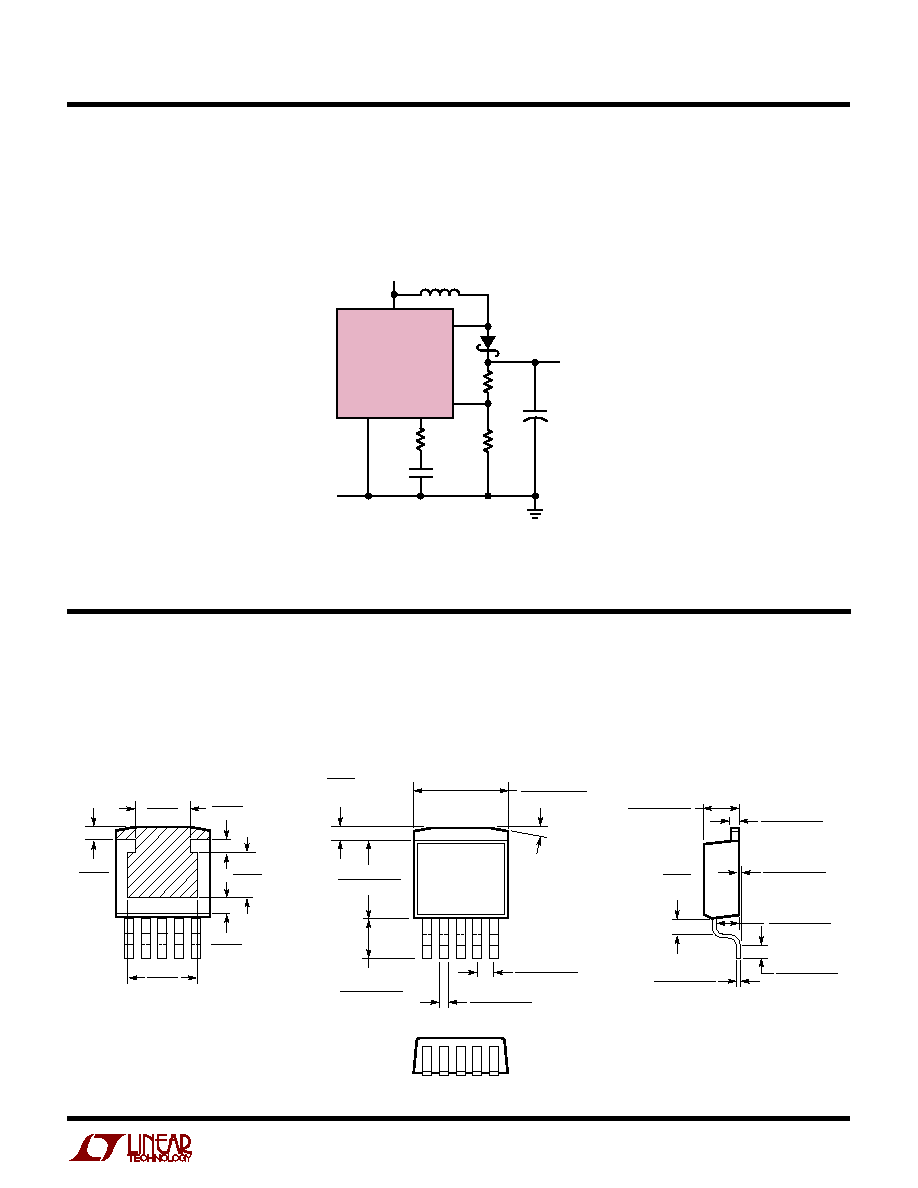
TYPICAL APPLICATIO
N
U
D
U
ESCRIPTIO
S
FEATURE
s
Wide Input Voltage Range 3.5V to 30V
s
Low Quiescent Current: 7mA
s
Internal 4A Switch
s
Very Few External Parts Required
s
Self Protected Against Overloads
s
Shutdown Mode Draws Only 100
µ
A Supply Current
s
Flyback Regulated Mode Has Fully Floating Outputs
s
Comes in Standard 5-Pin Package
s
Can Be Externally Synchronized (See LT1072 Data Sheet)
U
S
A
O
PPLICATI
s
Boost Converter
s
High Efficiency Buck Converter
s
PC Power Supply with Multiple Outputs
s
Battery Up-Converter
s
Negative-to-Positive Converter
USER NOTE:
This data sheet is only intended to provide specifications, graphs, and a general functional
description of the LT1271/LT1269. Application circuits are included to show the capability of the
LT1271/LT1269. A complete design manual (AN-19) should be obtained to assist in developing new
designs. This manual contains a comprehensive discussion of both the LT1070 and the external
components used with it, as well as complete formulas for calculating the values of these
components. The manual can also be used for the LT1271/LT1269 by factoring in the higher switch
current rating and higher operating frequency.
The LT
Æ
1271 and LT1269 are monolithic high power
switching regulators. Identical to the popular LT1070,
except for switching frequency (LT1271 = 60kHz, LT1269
= 100kHz) and slightly lower switch current, they can be
operated in all standard switching configurations includ-
ing buck, boost, flyback and inverting. A high current, high
efficiency switch is included on the die along with all
oscillator, control and protection circuitry. Integration of
all functions allows the LT1271/LT1269 to be built in a
standard TO-220 power package. This makes them ex-
tremely easy to use and provides "bust proof" operation
similar to that obtained with 3-pin linear regulators.
The LT1271/LT1269 operate with supply voltages from
3.5V to 30V, and draw only 7mA quiescent current. By
utilizing current mode switching techniques, they pro-
vides excellent AC and DC load and line regulation.
A patented adaptive antisat switch drive allows very wide
ranging load currents with no loss in efficiency. An exter-
nally activated shutdown mode reduces total supply cur-
rent to 100
µ
A typical for standby operation.
, LTC and LT are registered trademarks of Linear Technology Corporation.
Burst Mode is a trademark of Linear Technology Corporation.
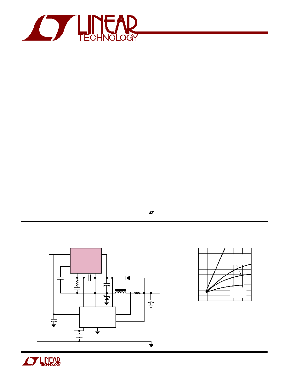
INPUT VOLTAGE (V)
0
0
OUTPUT POWER (W)
10
20
30
5
10
15
20
1271/69 TA02
25
40
50
30
BOOST
BUCK-BOOST
V
O
= 5V
(INVERTING)
FLYBACK
BUCK-BOOST
V
O
= 12V
(INVERTING)
BUCK MODE OUTPUT POWER
(3.5A)(V
OUT
)
TRANSFORMER TURNS RATIO MUST BE
OPTIMUM TO ACHIEVE FULL POWER.
Maximum Output Power
V
SW
FB
GND
V
IN
V
C
LT1271
C1
200
µ
F
35V
0.02
µ
F
0.1
µ
F
680
0.03
µ
F
4.7
µ
F
TANT
1N4148
L1
25
µ
H
TO 50
µ
H
0.015
390
µ
F
16V
V
OUT
5V, 3A
< 0.3V = NORMAL RUN MODE
> 2.5V = SHUTDOWN
OPEN = BURST MODE OPERATION
V
IN
6.5V TO 25V
127/691 TA01
V
C
V
IN
MODE
V
OUT
V
LIM
V
+
LT1432
GND
DIODE
MBR
330pF
EFFICIENCY
90%
AT I
OUT
= 0.4A TO 1.5A
+
+
+
High Efficiency 5V Regulator with Burst Mode
TM
Operation
2
LT1271/LT1269
A
U
G
W
A
W
U
W
A
R
BSOLUTE
XI
TI
S
Operating Junction Temperature Range
Operating .............................................. 0
∞
C to 100
∞
C
Short Circuit ......................................... 0
∞
C to 125
∞
C
Lead Temperature (Soldering, 10 sec.)................ 300
∞
C
Supply Voltage ....................................................... 30V
Switch Output Voltage ............................................ 60V
Feedback Pin Voltage (Transient, 1ms) ................
±
15V
Storage Temperature Range ................ ≠ 65
∞
C to 150
∞
C
W
U
U
PACKAGE/ORDER I FOR ATIO
ORDER PART
NUMBER
V
IN
V
SW
GND
FB
V
C
T PACKAGE
5-LEAD PLASTIC TO-220
FRONT VIEW
5
4
3
2
1
T
J MAX
= 100
∞
C,
JC
= 4
∞
C/W,
JA
= 50
∞
C/W
Q PACKAGE
5-LEAD PLASTIC DD
FRONT VIEW
V
IN
V
SW
GND
FB
V
C
5
4
3
2
1
T
J MAX
= 100
∞
C,
JC
= 4
∞
C/W,
JA
= 30
∞
C/W*
LT1271CQ
LT1269CQ
ORDER PART
NUMBER
LT1271CT
LT1269CT
ORDER PART
NUMBER
LT1269CS
WILL VARY FROM APPROXIMATELY 40
∞
C/W
WITH 0.75 SQ. IN. OF 1 OZ. COPPER TO 46
∞
C/W
WITH 0.33 SQ. IN. OF 1 OZ. COPPER
1
2
3
4
5
6
7
8
9
10
TOP VIEW
SW PACKAGE
20-LEAD PLASTIC WIDE SO
20
19
18
17
16
15
14
13
12
11
V
SW
V
SW
NC
GND
GND
GND
GND
AGND
V
C
FB
V
SW
V
SW
NC
GND
GND
GND
GND
V
IN
NC
NC
POWER
SWITCH
POWER
SWITCH
SYMBOL
PARAMETER
CONDITIONS
MIN
TYP
MAX
UNITS
V
REF
Reference Voltage
Measured at Feedback Pin
1.224
1.244
1.264
V
V
C
= 0.8V
q
1.214
1.244
1.274
V
I
B
Feedback Input Current
V
FB
= V
REF
350
750
nA
q
1100
nA
gm
Error Amplifier
I
C
=
±
25
µ
A
3000
4400
6000
µ
mho
Transconductance
q
2400
7000
µ
mho
Error Amplifier Source or
V
C
= 1.5V
150
200
350
µ
A
Sink Current
q
120
400
µ
A
Error Amplifier Clamp
Hi Clamp, V
FB
= 1V
1.8
2.3
V
Voltage
Lo Clamp, V
FB
= 1.5V
0.25
0.38
0.52
V
Reference Voltage Line
3V
V
IN
V
MAX,
V
C
= 0.8V
q
0.03
%/V
Regulation
A
V
Error Amplifier Voltage Gain
0.9V
V
C
1.4V
500
800
V/V
Minimum Input Voltage (Note 3)
q
2.8
3.0
V
I
Q
Supply Current
3V
V
IN
V
MAX
, V
C
= 0.6V
7
10
mA
V
IN
= 15V, V
C
= 0.5V, V
FB
= V
REF,
switch pin open, unless otherwise noted.
ELECTRICAL C
C
HARA TERISTICS
*With device soldered to 1/2 square inch of 1oz copper over backside or internal layer
ground plane. Consult factory for Industrial and Military grade parts.
3
LT1271/LT1269
SYMBOL
PARAMETER
CONDITIONS
MIN
TYP
MAX
UNITS
Control Pin Threshold
Duty Cycle = 0
0.7
0.9
1.08
V
q
0.5
1.25
V
Normal/Flyback Threshold
0.4
0.45
0.54
V
on Feedback Pin
V
FB
Flyback Reference Voltage
I
FB
= 50
µ
A
15
16.3
17.6
V
q
14
18
V
V
FB
Change in Flyback
0.05
I
FB
1mA
4.5
6.8
8.5
V
Reference Voltage
Flyback Reference Voltage
I
FB
= 50
µ
A
0.01
0.03
%/V
Line Regulation
3V
V
IN
V
MAX
Flyback Amplifier
I
C
=
±
10
µ
A
150
300
650
µ
mho
Transconductance (gm)
Flyback Amplifier Source
V
C
= 0.6V Source
q
15
32
70
µ
A
and Sink Current
I
FB
= 50
µ
A Sink
q
25
40
70
µ
A
BV
Output Switch Breakdown
3V
V
IN
V
MAX
q
60
75
V
Voltage
I
SW
= 1.5mA
V
SAT
Output Switch (Note 1)
q
0.2
0.33
"On" Resistance
Control Voltage to Switch
6.4
A/V
Current Transconductance
I
LIM
Switch Current Limit (Note 2)
Duty Cycle = 50%
q
4
8
A
Duty Cycle = 80%
q
3.2
8
A
I
IN
Supply Current Increase
25
40
mA/A
I
SW
During Switch On-Time
f
Switching Frequency
LT1271
q
50
60
70
kHz
LT1269
q
85
100
115
kHz
DC (max)
Maximum Switch Duty Cycle
LT1271
85
92
95
%
LT1269
80
90
95
%
Flyback Sense Delay Time
1.5
µ
s
Shutdown Mode
3V
V
IN
V
MAX
, V
C
= 0.05V
100
400
µ
A
Supply Current
Shutdown Mode
3V
V
IN
V
MAX
100
150
250
mV
Threshold Voltage
q
50
300
mV
ELECTRICAL C
C
HARA TERISTICS
V
IN
= 15V, V
C
= 0.5V, V
FB
= V
REF,
switch pin open, unless otherwise noted.
The
q
denotes the specifications which apply over the full operating
temperature range.
Note 1: Measured with V
C
in hi clamp, V
FB
= 0.8V.
Note 2: For duty cycles (DC) between 50% and 85%, minimum
guaranteed switch current is given by I
LIM
= 2.67 (2 ≠ DC).
Note 3: Minimum input voltage.
4
LT1271/LT1269
C
C
HARA TERISTICS
U
W
A
TYPICAL PERFOR
CE
Switch Current Limit vs Duty Cycle
Switch Saturation Voltage
DUTY CYCLE (%)
0
SWITCH CURRENT (A)
9
12
40
1271/69 G01
6
3
0
10
20 30
50 60 70 80 90 100
≠55
∞
C
125
∞
C
25
∞
C
SWITCH CURRENT (A)
0
0.4
SWITCH SATURATION VOLTAGE (V)
0.6
0.8
1.0
1.2
1.4
1.6
1
2
3
4
1271/69 G02
5
0.2
0
T
J
= 25
∞
C
U
S
A
O
PPLICATI
TYPICAL
C1
0.22
µ
F
L1**
100
µ
H
D1
MBR340
1271/69 TA04
LT1271
V
SW
FB
GND
V
IN
V
C
C2
200
µ
F
* REQUIRED IF INPUT LEADS
2"
** COILTRONICS CTX100-2-52
◊
◊
R1
11.3k
Q1
2N3906
OPTIONAL
OUTPUT
FILTER
L2
C3
R3
2.2k
V
IN
≠12V
V
OUT
12V, 1.5A
C4*
200
µ
F
OPTIONAL
INTPUT
FILTER
L3
R2
1.24k
+
+
Negative-to-Positive Buck-Boost Converter
5
LT1271/LT1269
U
S
A
O
PPLICATI
TYPICAL
Boost Converter (5V to 12V)
1
µ
F
100
µ
H*
MBR330
10.7k
1271/69 TA03
5V
12V
0.5A
LT1271
V
SW
FB
GND
V
IN
V
C
1.24k
100
µ
F
25V
1k
* COILTRONICS CTX100-2-52
+
U
PACKAGE DESCRIPTIO
Dimensions in inches (millimeters) unless otherwise noted.
Q Package
5-Lead Plastic DD Pak
(LTC DWG # 05-08-1461)
Q(DD5) 0396
0.028 ≠ 0.038
(0.711 ≠ 0.965)
0.143
+0.012
≠0.020
(
)
3.632
+0.305
≠0.508
0.057 ≠ 0.077
(1.447 ≠ 1.955)
0.013 ≠ 0.023
(0.330 ≠ 0.584)
0.095 ≠ 0.115
(2.413 ≠ 2.921)
0.004
+0.008
≠0.004
(
)
0.102
+0.203
≠0.102
0.050
±
0.012
(1.270
±
0.305)
0.059
(1.499)
TYP
0.045 ≠ 0.055
(1.143 ≠ 1.397)
0.165 ≠ 0.180
(4.191 ≠ 4.572)
0.330 ≠ 0.370
(8.382 ≠ 9.398)
0.060
(1.524)
TYP
0.390 ≠ 0.415
(9.906 ≠ 10.541)
15
∞
TYP
0.300
(7.620)
0.075
(1.905)
0.183
(4.648)
0.060
(1.524)
0.060
(1.524)
0.256
(6.502)
BOTTOM VIEW OF DD PAK
HATCHED AREA IS SOLDER PLATED
COPPER HEAT SINK