 | ÐлекÑÑоннÑй компоненÑ: LT1300CN8 | СкаÑаÑÑ:  PDF PDF  ZIP ZIP |
Äîêóìåíòàöèÿ è îïèñàíèÿ www.docs.chipfind.ru
1
LT1300
s
Up to 220mA Output Current at 5V from 2V Supply
s
Supply Voltage as Low as 1.8V
s
Up to 88% Efficiency
s
Small Inductor 10
µ
H
s
120
µ
A Quiescent Current
s
Shutdown to 10
µ
A
s
Programmable 3.3V or 5V Output
s
I
LIM
Pin Programs Peak Switch Current
s
Low V
CESAT
Switch: 170mV at 1A Typical
s
Uses Inexpensive Surface Mount Inductors
s
8-Lead DIP or SOIC Package
s
Palmtop Computers
s
Portable Instruments
s
Bar-Code Scanners
s
DC/DC Converter Module Replacements
s
Battery Backup Supplies
s
Personal Digital Assistants
s
PCMCIA Cards
The LT1300 is a micropower step-up DC/DC converter that
utilizes Burst ModeTM operation. The device can deliver 5V
or 3.3V from a two-cell battery input. It features program-
mable 5V or 3.3V output via a logic-controlled input, no-
load quiescent current of 120
µ
A and a shutdown pin which
reduces supply current to 10
µ
A. The on-chip power switch
has a low 170mV saturation voltage at a switch current of
1A, a four-fold reduction over prior designs. A 155kHz
internal oscillator allows the use of extremely small sur-
face mount inductors and capacitors. Operation is guaran-
teed at 1.8V input. This allows more energy to be extracted
from the battery increasing operating life. The I
LIM
pin can
be used to program peak switch current with a single
resistor allowing the use of less expensive and smaller
inductors and capacitors in lighter load applications. The
LT1300 is available in an 8-lead SOIC package, minimizing
board space requirements. For a 5V/12V Selectable Out-
put Converter see the LT1301. For increased output cur-
rent see the LT1302.
DESCRIPTIO
N
U
FEATURES
TYPICAL APPLICATIO
N
S
N
U
Micropower High Efficiency
3.3/5V Step-Up DC/DC Converter
APPLICATIO
N
S
U
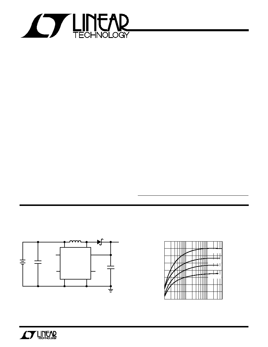
Two-Cell to 3.3V/5V Step-Up Converter
5V Output Efficiency
L1 = COILCRAFT DO1608-103
OR SUMIDA CD54-100
C1 = AVX TPSD107M010R0100
OR SANYO OS-CON 16SA100M
D1 = MBRS130LT3
OR 1N5817
C1
100µF
5V/3.3V
OUTPUT
+
+
L1
10µH
D1
C1
100µF
2
×
AA
CELL
SW
I
LIM
PGND
GND
SENSE
LT1300
SELECT
LT1300 TA1
5V/3.3V
SELECT
SHDN
SHUTDOWN
N/C
2
6
7
4
5
8
1
3
V
IN
LOAD CURRENT (mA)
10
100
500
LT1300 TA2
1
74
EFFICIENCY (%)
76
78
80
82
90
84
86
88
V
IN
= 4.0V
V
IN
= 3.0V
V
IN
= 2.5V
V
IN
= 2.0V
Burst Mode is a trademark of Linear Technology Corporation.
2
LT1300
ORDER PART
NUMBER
ABSOLUTE
M
AXI
M
U
M
RATINGS
W
W
W
U
PACKAGE/ORDER I
N
FOR
M
ATIO
N
W
U
U
V
IN
Voltage .............................................................. 10V
SW1 Voltage ............................................................ 20V
Sense Voltage .......................................................... 10V
SHUTDOWN Voltage................................................ 10V
SELECT Voltage ....................................................... 10V
I
LIM
Voltage ............................................................ 0.5V
Maximum Power Dissipation ............................. 500mW
Operating Temperature Range ..................... 0
°
C to 70
°
C
Storage Temperature Range ................. 65
°
C to 150
°
C
Lead Temperature (Soldering, 10 sec).................. 300
°
C
S8 PART MARKING
T
JMAX
= 100
°
C,
JA
= 150
°
C/ W
1300
LT1300CN8
LT1300CS8
Consult factory for Industrial grade parts.
SYMBOL
PARAMETER
CONDITIONS
MIN
TYP
MAX
UNITS
I
Q
Quiescent Current
V
SHDN
= 0.5V, V
SEL
= 5V, V
SENSE
= 5.5V
q
120
200
µ
A
V
SHDN
= 1.8V
q
7
15
µ
A
V
IN
Input Voltage Range
1.8
V
q
2.0
V
V
OUT
Output Sense Voltage
V
SEL
= 5V
q
4.80
5.0
5.20
V
V
SEL
= 0V
q
3.15
3.3
3.45
V
Output Referred
V
SEL
= 5V (Note 1)
q
22
50
mV
Comparator Hysteresis
V
SEL
= 0V (Note 1)
q
14
35
mV
Oscillator Frequency
Current Limit not Asserted. See Test Circuit.
120
155
185
kHz
Oscillator TC
0.2
%/
°
C
DC
Maximum Duty Cycle
75
86
95
%
t
ON
Switch On Time
Current Limit not Asserted.
5.6
µ
s
Output Line Regulation
1.8V < V
IN
< 6V
q
0.06
0.15
%/V
V
CESAT
Switch Saturation Voltage
I
SW
= 700mA
q
130
200
mV
Switch Leakage Current
V
SW
= 5V, Switch Off
q
0.1
10
µ
A
Peak Switch Current
I
LIM
Floating (See Typical Application)
0.75
1.0
1.25
A
(Internal Trip Point)
I
LIM
Grounded
0.4
A
V
SHDNH
Shutdown Pin High
q
1.8
V
V
SHDNL
Shutdown Pin Low
0.5
V
V
SELH
Select Pin High
q
1.5
V
V
SELL
Select Pin Low
q
0.8
V
I
SHDN
Shutdown Pin Bias Current
V
SHDN
= 5V
q
9
20
µ
A
V
SHDN
= 2V
q
3
µ
A
V
SHDN
= 0V
q
0.1
1
µ
A
I
SEL
Select Pin Bias Current
0V < V
SEL
< 5V
q
1
3
µ
A
ELECTRICAL CHARACTERISTICS
T
A
= 25
°
C, V
IN
= 2V unless otherwise noted.
Note 1: Hysteresis specified is DC. Output ripple may be higher if
output capacitance is insufficient or capacitor ESR is excessive. See
applications section.
The
q
denotes specifications which apply over the 0
°
C to 70
°
C
temperature range.
1
2
3
4
8
7
6
5
TOP VIEW
GND
SEL
SHDN
SENSE
PGND
SW
V
IN
I
LIM
N8 PACKAGE
8-LEAD PLASTIC DIP
S8 PACKAGE
8-LEAD PLASTIC SOIC
3
LT1300
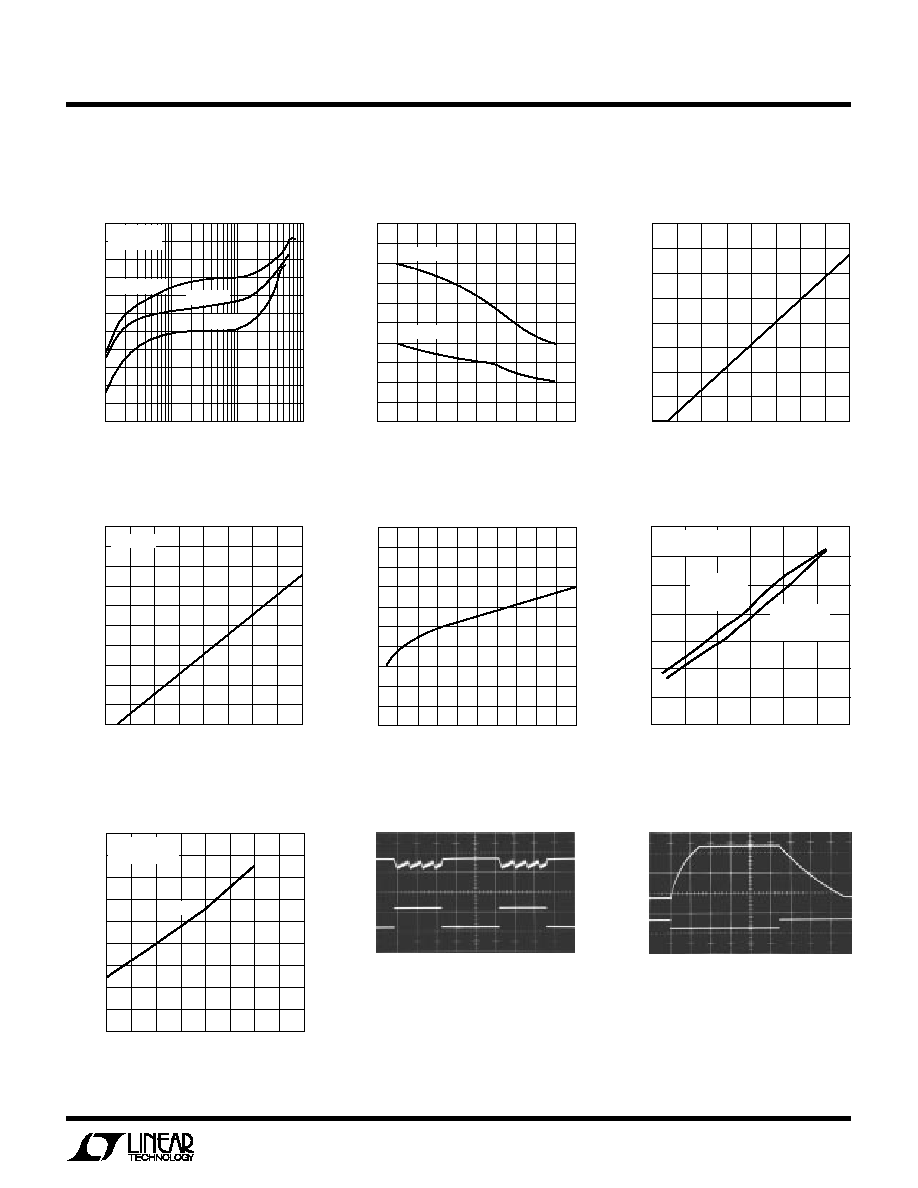
TYPICAL PERFOR
M
A
N
CE CHARACTERISTICS
U
W
No-Load Battery Current
Total Quiescent Current
in Shutdown
SWITCH CURRENT (A)
0
0.1
V
CESAT
(mV)
150
125
200
175
250
225
0.8 0.9
LT1300 G5
100
75
50
25
0
0.2 0.3 0.4 0.5 0.6 0.7
1
Maximum Output Current
vs Input Voltage
Maximum Output Current
vs Input Voltage
200
µ
s/DIV
0
Transient Response
V
IN
= 2V, V
OUT
= 5V
Startup Response
V
CESAT
vs I
SW
Efficiency
Shutdown Pin Bias Current
V
OUT
100mV/DIV
AC COUPLED
V
OUT
1V/DIV
V
SHDN
10V/DIV
LT1300 G8
SHUTDOWN VOLTAGE (V)
0
0
SHUTDOWN CURRENT (µA)
2
6
8
10
20
14
2
4
5
LT1300 G4
4
16
18
12
1
3
6
7
8
T
A
= 25°C
LOAD CURRENT (mA)
1
74
EFFICIENCY (%)
76
78
80
82
10
100
1000
LT1300 G1
72
70
68
66
84
86
88
V
IN
= 3V
V
IN
= 2V
V
IN
= 2.5V
V
OUT
= 3.3V
L = 10µH
INPUT VOLTAGE (V)
1.4
INPUT CURRENT (µA)
150
145
160
155
170
165
3.0
2.8
LT1300 G2
140
135
130
125
120
1.8
1.6
2.2
2.0
2.6
2.4
3.4
3.2
V
OUT
= 5V
V
OUT
= 3.3V
INPUT VOLTAGE (V)
0
I
SHDN
+
I
VIN
+
I
SENSE
(µA)
40
50
60
8
LT1300 G3
30
20
0
2
4
6
10
80
70
1
3
5
7
INPUT VOLTAGE (V)
1.5
OUTPUT CURRENT (mA)
500
600
700
3
4
LT1300 G6
400
300
2
2.5
3.5
4.5
200
100
0
V
OUT
= 5V,
I
LIM
FLOATING
L = 22µH
COILCRAFT
DO3316-223
L = 10µH
COILCRAFT
DO1608-103
INPUT VOLTAGE (V)
1.5
0
LOAD CURRENT (mA)
100
300
400
500
2.5
3
3.5
900
LT1300 G7
200
2
600
700
800
L = 10µH
VOUT = 3.3V
ILIM FLOATING
V
OUT
= 5V
R
LOAD
= 20
LT1300 G9
500
µ
s/DIV
200mA
I
LOAD
4
LT1300
PI
N
FU
N
CTIO
N
S
U
U
U
GND (Pin 1): Signal Ground.
Sel (Pin 2): Output Select. When tied to V
IN
or V
OUT
converter regulates at 5V. When grounded converter
regulates at 3.3V.
SHDN (Pin 3): Shutdown. Pull high to effect shutdown. Tie
to ground for normal operation.
Sense (Pin 4): "Output" Pin.
I
LIM
(Pin 5): Float for 1A switch current limit. Tie to ground
for approximately 400mA. A resistor between I
LIM
and
ground sets peak current to some intermediate value (see
Figure 5).
V
IN
(Pin 6): Supply Pin. Must be bypassed with a large
value electrolytic to ground. A 0.1
µ
F ceramic capacitor
close to the pin may be needed in some cases.
SW (Pin 7): Switch Pin. Connect inductor and diode here.
Keep layout short and direct to minimize electronic radia-
tion.
PGND (Pin 8): Power Ground. Tie to signal ground (pin 1)
under the package. Bypass capacitor from V
IN
should be
tied directly to the pin.
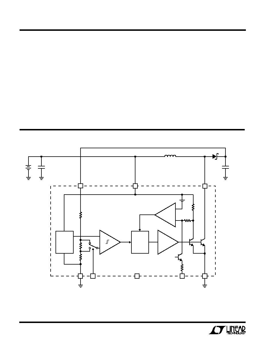
Figure 1.
BLOCK DIAGRA
M
W
OSCILLATOR
155kHZ
R2
730
C2
SW
R1
3
Q2
1x
Q1
160x
18mV
OFF
V
IN
V
IN
I
LIM
PGND
V
OUT
ENABLE
A1
COMPARATOR
+
+
+
+
1.25V
REFERENCE
L1
D1
7
2
4
SENSE
A2 CURRENT
COMPARATOR
A3 DRIVER
BIAS
Q3
8.5k
5
8
SHUTDOWN
3
SELECT
2
GND
161k
144k
500k
C1
1
LT1300 F1
5
LT1300
TEST CIRCUITS
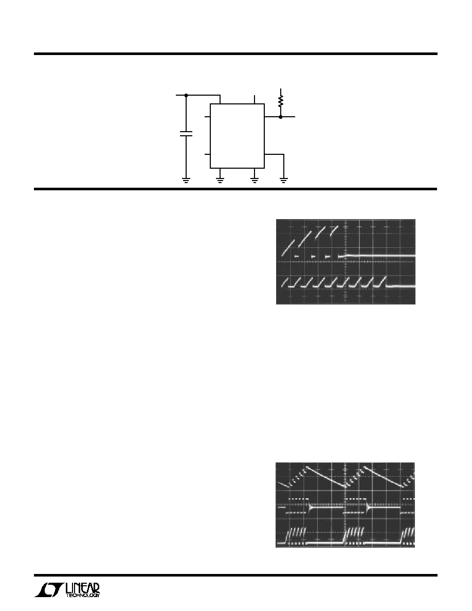
Oscillator Test Circuit
OPERATIO
N
U
20
µ
s/DIV
reduced by tying the I
LIM
pin to ground, causing 15
µ
A to
flow through R2 into Q3's collector. Q3's current causes
a 10.4mV drop in R2 so that only an additional 7.6mV is
required across R1 to turn off the switch. This corre-
sponds to a 400mA switch current as shown in Figure 2,
trace B. The reduced peak switch current reduces I
2
R
loses in Q1, L1, C1 and D1. Efficiency can be increased by
doing this provided that the accompanying reduction in
full load output current is acceptable. Lower peak currents
also extend alkaline battery life due to the alkaline cell's
high internal impedance. Typical operating waveforms are
shown in Figure 3.
Operation of the LT1300 is best understood by referring to
the Block Diagram in Figure 1. When A1's negative input,
related to the Sense pin voltage by the appropriate resis-
tor-divider ratio, is higher that the 1.25V reference voltage,
A1's output is low. A2, A3 and the oscillator are turned off,
drawing no current. Only the reference and A1 consume
current, typically 120
µ
A. When the voltage at A1's nega-
tive input decreases below 1.25V, overcoming A1's 6mV
hysteresis, A1's output goes high, enabling the oscillator,
current comparator A2, and driver A3. Quiescent current
increases to 2mA as the device prepares for high current
switching. Q1 then turns on in a controlled saturation for
(nominally) 5.3
µ
s or until current comparator A2 trips,
whichever comes first. After a fixed off-time of (nominally)
1.2
µ
s, Q1 turns on again. The LT1300's switching causes
current to alternately build up in L1 and dump into capaci-
tor C2 via D1, increasing the output voltage. When the
output is high enough to cause A1's output to go to low,
switching action ceases. C2 is left to supply current to the
load until V
OUT
decreases enough to force A1's output
high, and the entire cycle repeats.
If switch current reaches 1A, causing A2 to trip, switch on-
time is reduced and off-time increases slightly. This allows
continuous mode operation during bursts. Current com-
parator A2 monitors the voltage across 3
resistor R1
which is directly related to inductor L1's current. Q2's
collector current is set by the emitter-area ratio to 0.6%
of Q1's collector current. When R1's voltage drop exceeds
18mV, corresponding to 1A inductor current, A2's output
goes high, truncating the on-time portion of the oscillator
cycle and increasing off-time to about 2
µ
s as shown in
Figure 2, trace A. This programmed peak current can be
Figure 3. Burst Mode Operation in Action
TRACE B
500mA/DIV
I
LIM
PIN
GROUNDED
LT1300 F2
Figure 2. Switch Pin Current With I
LIM
Floating or Grounded
TRACE A
500mA/DIV
I
LIM
PIN
OPEN
V
OUT
20mV/DIV
AC COUPLED
V
SW
5V/DIV
I
SW
IA/DIV
20
µ
S/DIV
LT1300 F2
2V
100µF
V
IN
SEL
SENSE
GND
PGND
SHDN
SW
LT1300
I
L
100
5V
f
OUT