 | ÐлекÑÑоннÑй компоненÑ: LT1302C-5 | СкаÑаÑÑ:  PDF PDF  ZIP ZIP |
/home/web/doc/html/liner/177537
1
LT1302/LT1302-5
Micropower
High Output Current
Step-Up Adjustable and
Fixed 5V DC/DC Converters
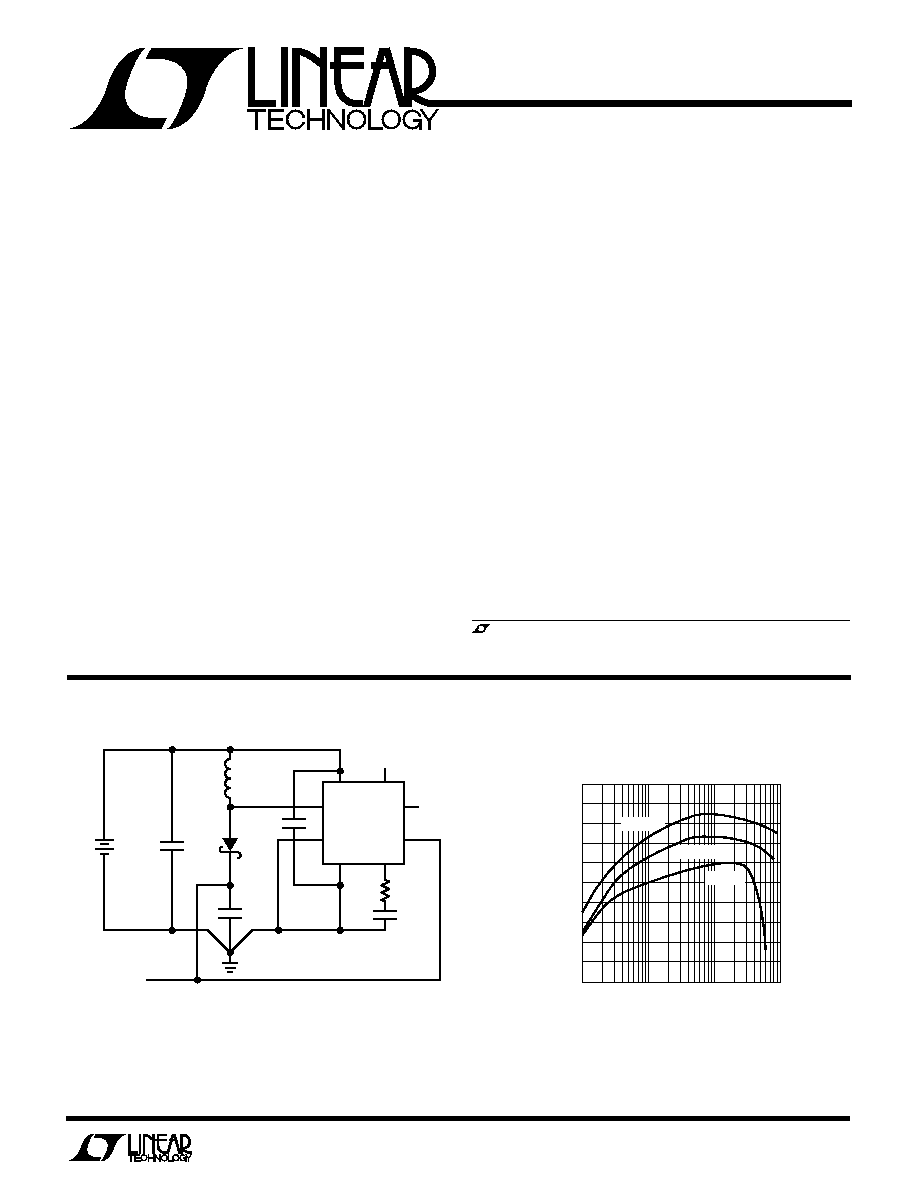
Figure 1. 2-Cell to 5V/600mA DC/DC Converter
S
FEATURE
D
U
ESCRIPTIO
s
5V at 600mA or 12V at 120mA from 2-Cell Supply
s
200
µ
A Quiescent Current
s
Logic Controlled Shutdown to 15
µ
A
s
Low V
CESAT
Switch: 310mV at 2A Typical
s
Burst Mode
TM
Operation at Light Load
s
Current Mode Operation for Excellent
Line and Load Transient Response
s
Available in 8-Lead SO or PDIP
s
Operates with Supply Voltage as Low as 2V
The LT
®
1302/LT1302-5 are micropower step-up DC/DC
converters that maintain high efficiency over a wide
range of output current. They operate from a supply
voltage as low as 2V and feature automatic shifting
between Burst Mode operation at light load, and current
mode operation at heavy load.
The internal low loss NPN power switch can handle
current in excess of 2A and switch at frequencies up to
400kHz. Quiescent current is just 200
µ
A and can be
further reduced to 15
µ
A in shutdown.
Available in 8-pin PDIP or 8-pin SO packaging, the LT1302/
LT1302-5 have the highest switch current rating of any
similarly packaged switching regulators presently on the
market.
U
S
A
O
PPLICATI
, LTC and LT are registered trademarks of Linear Technology Corporation.
Burst Mode is a trademark of Linear Technology Corporation.
s
Notebook and Palmtop Computers
s
Portable Instruments
s
Personal Digital Assistants
s
Cellular Telephones
s
Flash Memory
U
A
O
PPLICATI
TYPICAL
+
NC
C3
0.1
µ
F
SHUTDOWN
V
IN
I
T
V
C
SW
PGND
SHDN
SENSE
GND
2
R
C
20k
C
C
0.01
µ
F
C1
100
µ
F
D1
+
C2
100
µ
F
L1
10
µ
H
2 CELLS
LT1302 · F01
C1 = C2 = SANYO OS-CON
L1 = COILTRONICS CTX10-3
COILCRAFT DO3316-103
OUTPUT
5V
600mA
1
8
7
6
5
3
4
D1 = MOTOROLA MBRS130LT3
LT1302-5
LOAD CURRENT (mA)
1
78
EFFICIENCY (%)
80
82
84
86
10
100
1000
LT1302 · TA02
76
74
72
70
88
90
V
IN
= 3V
V
IN
= 2.5V
V
IN
= 2V
2-Cell to 5V Converter Efficiency
2
LT1302/LT1302-5
A
U
G
W
A
W
U
W
A
R
BSOLUTE
XI
TI
S
W
U
U
PACKAGE/ORDER I FOR ATIO
V
IN
Voltage ............................................................. 10V
SW Voltage ............................................................. 25V
FB Voltage .............................................................. 10V
SHDN Voltage ......................................................... 10V
V
C
Voltage ................................................................ 4V
I
T
Voltage .................................................................. 4V
Maximum Power Dissipation ............................ 700mW
Operating Temperature Range .................... 0
°
C to 70
°
C
Storage Temperature Range ............... 65
°
C to 150
°
C
Lead Temperature (Soldering, 10 sec)................. 300
°
C
Consult factory for Industrial and Military grade parts.
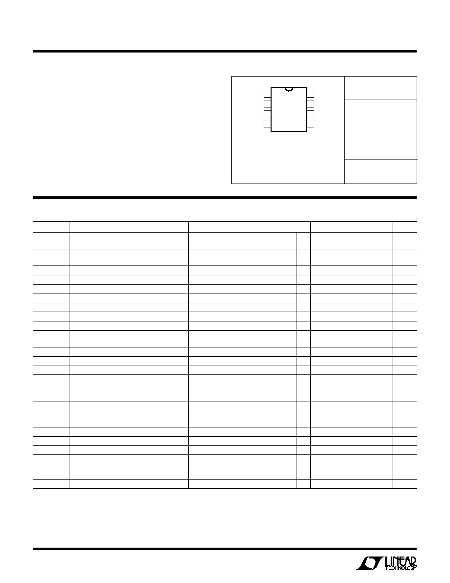
ORDER PART
NUMBER
LT1302CN8
LT1302CS8
LT1302CN8-5
LT1302CS8-5
S8 PART MARKING
1302
13025
SYMBOL
PARAMETER
CONDITIONS
MIN
TYP
MAX
UNITS
I
Q
Quiescent Current
V
SHDN
= 0.5V, V
FB
= 1.3V
q
200
300
µ
A
V
SHDN
= 1.8V
q
15
25
µ
A
V
IN
Input Voltage Range
2.0
V
q
2.2
8
V
V
FB
Feedback Voltage (LT1302)
V
C
= 0.4V
q
1.22
1.24
1.26
V
Feedback Pin Bias Current (LT1302)
V
FB
= 1V
100
nA
Output Sense Voltage (LT1302-5)
V
C
= 0.4V
q
4.85
5.05
5.25
V
Output Ripple Voltage (LT1302-5)
V
C
= 0.4V
50
mV
Sense Pin Resistance to Ground (LT1302-5)
420
k
V
OS
Offset Voltage
See Block Diagram
15
mV
Comparator Hysteresis
(Note 1)
5
mV
Oscillator Frequency
Current Limit Not Asserted (Note 2)
175
220
265
kHz
q
160
310
kHZ
DC
Maximum Duty Cycle
75
86
95
%
t
ON
Switch On Time
Current Limit Not Asserted
3.9
µ
s
t
OFF
Switch Off Time
0.7
µ
s
Output Line Regulation
2 < V
IN
< 8V
q
0.06
0.15
%/V
V
CESAT
Switch Saturation Voltage
I
SW
= 2A
310
400
mV
q
475
mV
Switch Leakage Current
V
SW
= 5V, Switch Off
q
0.1
10
µ
A
Switch Current Limit
V
C
= 0.4V (Burst Mode Operation)
1
A
V
C
= 1.25V (Full Power) (Note 3)
q
2.0
2.8
3.9
A
Error Amplifier Voltage Gain
0.9V
V
C
1.2V,
V
C
/
V
FB
50
75
V/ V
V
SHDNH
Shutdown Pin High
q
1.8
V
V
SHDNL
Shutdown Pin Low
q
0.5
V
I
SHDN
Shutdown Pin Bias Current
V
SHDN
= 5V
q
8
20
µ
A
V
SHDN
= 2V
3
µ
A
V
SHDN
= 0V
q
0.1
1
µ
A
I
T
Pin Resistance to Ground
3.9
k
T
A
= 25
°
C, V
IN
= 2.5V, unless otherwise noted.
ELECTRICAL C
C
HARA TERISTICS
C
D
The
q
denotes specifications which apply over the 0
°
C to 70
°
C
temperature range.
Note 1: Hysteresis is specified at DC. Output ripple depends on capacitor
size and ESR.
Note 2: The LT1302 operates in a variable frequency mode. Switching
frequency depends on load inductance and operating conditions and may
be above specified limits.
Note 3: Minimum switch current 100% tested. Maximum switch current
guaranteed by design.
1
2
3
4
8
7
6
5
TOP VIEW
GND
V
C
SHDN
(SENSE*)FB
PGND
SW
V
IN
I
T
N8 PACKAGE
8-LEAD PDIP
S8 PACKAGE
8-LEAD PLASTIC SO
*FIXED VERSION
PINS 1 AND 8 ARE INTERNALLY
CONNECTED IN SOIC PACKAGE
T
JMAX
= 125
°
C,
JA
= 100
°
C/W (N8)
T
JMAX
= 125
°
C,
JA
= 80
°
C/W (S8)
3
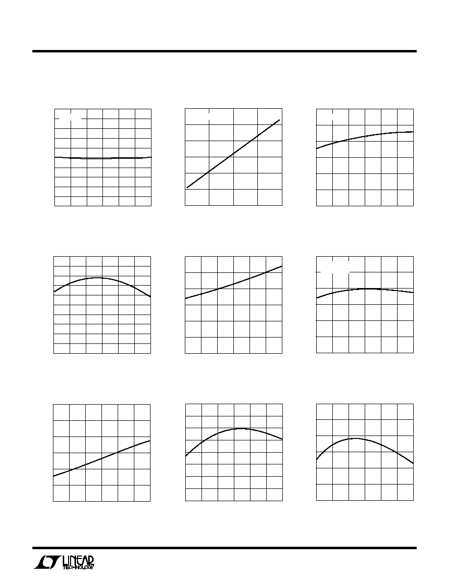
LT1302/LT1302-5
TYPICAL PERFOR
M
A
N
CE CHARACTERISTICS
U
W
TEMPERATURE (
°
C)
50
SATURATION VOLTAGE (mV)
400
350
300
250
200
150
100
25
0
25
50
1302 G03
75
100
I
SW
= 2A
TEMPERATURE (
°
C)
50
FEEDBACK VOLTAGE (V)
1.250
1.245
1.240
1.235
1.230
1.225
1.220
1.215
1.210
1.205
1.200
25
0
25
50
1302 G04
75
100
SUPPLY VOLTAGE (V)
2.0
2.5
3.0
3.5
4.0
4.5
5.0
QUIESCENT CURRENT (
µ
A)
500
450
400
350
300
250
200
150
100
50
0
1302 G01
T
A
= 25
°
C
No-Load Quiescent Current
Circuit of Figure 1
TEMPERATURE (
°
C)
50
SENSE RESISTANCE (k
)
600
500
400
300
200
100
0
25
0
25
50
1302 G05
75
100
TEMPERATURE (
°
C)
50
QUIESCENT CURRENT (
µ
A)
300
250
200
150
100
50
0
25
0
25
50
1302 G06
75
100
V
IN
= 2.5V
SWITCH OFF
TEMPERATURE (
°
C)
50
OFFSET VOLTAGE (mV)
30
25
20
15
10
5
0
25
0
25
50
1302 G07
75
100
TEMPERATURE (
°
C)
50
OUTPUT VOLTAGE (V)
5.100
5.075
5.050
5.025
5.000
4.975
4.950
4.925
4.900
25
0
25
50
1302 G08
75
100
TEMPERATURE (
°
C)
50
ON-TIME (
µ
s)
5.0
4.5
4.0
3.5
3.0
2.5
2.0
25
0
25
50
1302 G09
75
100
SWITCH CURRENT (A)
0
V
CESAT
(V)
600
500
400
300
200
100
0
1
2
3
4
1302 G02
T
A
= 25
°
C
Switch Saturation Voltage
Switch Saturation Voltage
LT1302 Feedback Voltage
LT1302-5 Sense Pin Resistance
Quiescent Current
Error Amplifier Offset Voltage
LT1302-5 Output Voltage
Maximum On-Time
4
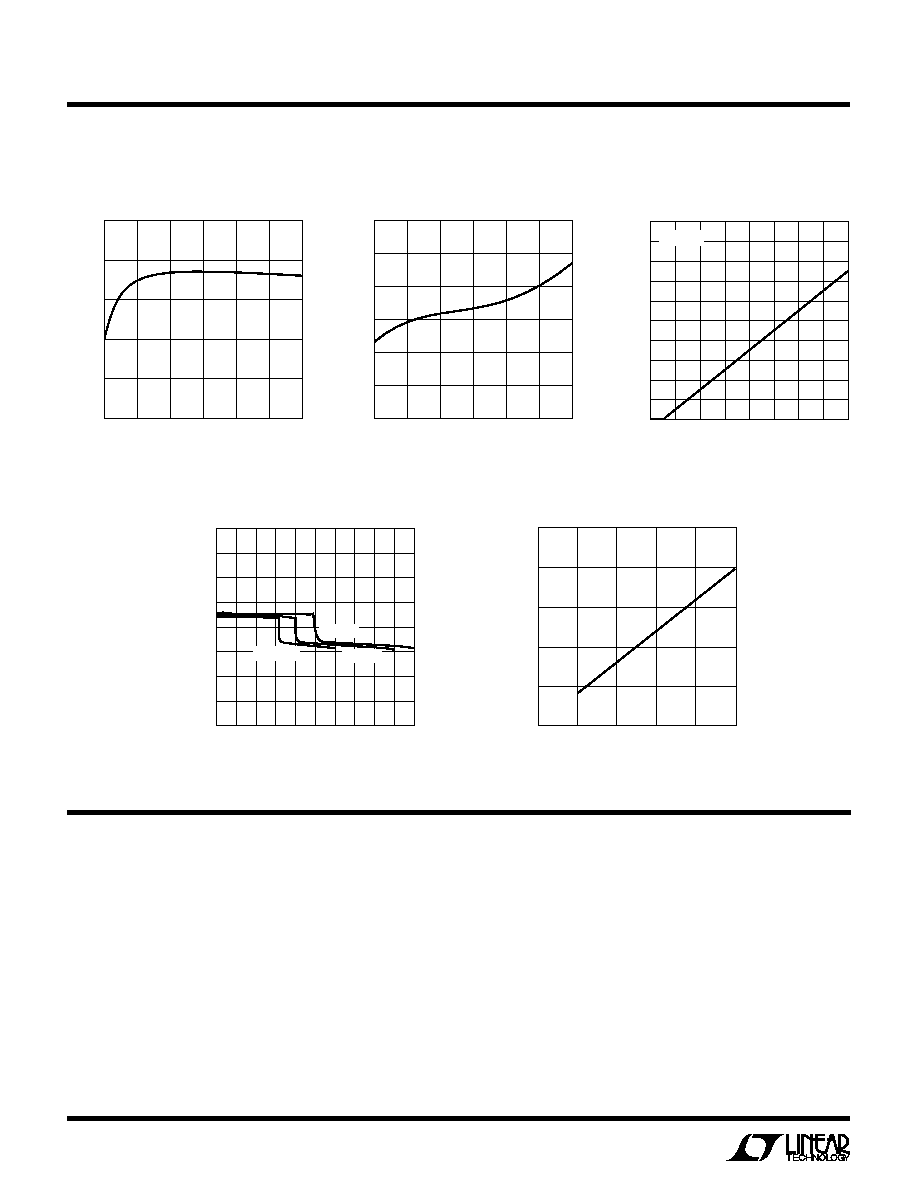
LT1302/LT1302-5
TYPICAL PERFOR
M
A
N
CE CHARACTERISTICS
U
W
TEMPERATURE (
°
C)
50
DUTY CYCLE (%)
100
90
80
70
60
50
25
0
25
50
1302 G10
75
100
TEMPERATURE (
°
C)
50
FREQUENCY (kHz)
300
275
250
225
200
175
150
25
0
25
50
1302 G11
75
100
SHUTDOWN VOLTAGE (V)
0
SHUTDOWN CURRENT (
µ
A)
20
18
16
14
12
10
8
6
4
2
0
4
5
1302 G12
1
3
2
6
7
8
T
A
= 25
°
C
GND (Pin 1): Signal Ground. Feedback resistor and 0.1
µ
F
ceramic bypass capacitor from V
IN
should be connected
directly to this pin.
V
C
(Pin 2): Frequency Compensation Pin. Connect series
RC to GND. Keep trace short.
SHDN (Pin 3): Shutdown. Pull high to effect shutdown; tie
to ground for normal operation.
FB/Sense (Pin 4): Feedback/Sense. On the LT1302 this
pin connects to CMP1 input. On the LT1302-5 this pin
connects to the output resistor string.
PI FU CTIO S
U
U
U
I
T
(Pin 5): Normally left floating. Addition of a 3.3k resistor
to GND forces the LT1302 into current mode at light loads.
Efficiency drops at light load but increases at medium
loads. See Applications Information section.
V
IN
(Pin 6): Supply Pin. Must be bypassed with: (1) a 0.1
µ
F
ceramic to GND, and (2) a large value electrolytic to PGND.
When V
IN
is greater than 5V, a low value resistor (2
to
10
) is recommended to isolate the V
IN
pin from input
supply noise.
Maximum Duty Cycle
Oscillator Frequency
Shutdown Pin Bias Current
LT1302-5 Output Voltage vs
Load Current
LOAD CURRENT (A)
0
OUTPUT VOLTAGE (V)
5.20
5.15
5.10
5.05
5.00
4.95
4.90
4.85
4.80
0.1 0.2 0.3 0.4
1302 G13
0.5 0.6 0.7 0.8 0.9 1.0
V
IN
= 2.2V
V
IN
= 3V
V
IN
= 4V
Maximum Output Power*
Boost Mode
INPUT VOLTAGE (V)
0
OUTPUT POWER (W)
20
16
12
8
4
0
8
1302 G14
2
4
* APPROXIMATE
6
10
5
LT1302/LT1302-5
PI FU CTIO S
U
U
U
SW (Pin 7): Switch Pin. Connect inductor and diode here.
Keep layout short and direct.
PGND (Pin 8): Power Ground. Pins 8 and 1 should be
connected under the package. In the SO package, pins 1
and 8 are thermally connected to the die. One square inch
of PCB copper provides an adequate heat sink for the
device.
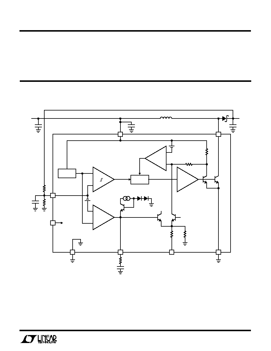
Figure 2. LT1302 Block Diagram
1302 F02
+
+
+
V
OS
15mV
R2
C5
100pF
36mV
CMP1
OFF
V
IN
2
µ
A
ENABLE
A2
V
IN
C2
0.1
µ
F
C1
V
IN
L1
SW
PGND
I
T
V
C
R3
22k
C4
0.01
µ
F
GND
SHDN
SHUTDOWN
FB
ERROR
AMPLIFIER
HYSTERETIC
COMPARATOR
DRIVER
A1
4
3
5
8
7
2
1
1.24V
REFERENCE
220kHz
OSCILLATOR
300
3.6k
Q3
R4
1.75
R5
730
V
IN
BIAS
R1
6
+
C3
D1
V
OUT
+
Q4
160X
A3
Q1
Q2
Q5
BLOCK DIAGRA S
M
W