Äîêóìåíòàöèÿ è îïèñàíèÿ www.docs.chipfind.ru
1
LT1304/LT1304-3.3/LT1304-5
Micropower
DC/DC Converters with
Low-Battery Detector
Active in Shutdown
The LT
®
1304 is a micropower step-up DC/DC converter
ideal for use in small, low voltage, battery-operated sys-
tems. The devices operate from a wide input supply range
of 1.5V to 8V. The LT1304-3.3 and LT1304-5 generate
regulated outputs of 3.3V and 5V and the adjustable
LT1304 can deliver output voltages up to 25V. Quiescent
current, 120
µ
A in active mode, decreases to just 10
µ
A in
shutdown with the low-battery detector still active. Peak
switch current, internally set at 1A, can be reduced by
adding a single resistor from the I
LIM
pin to ground. The
high speed operation of the LT1304 allows the use of
small, surface-mountable inductors and capacitors. The
LT1304 is available in an 8-lead SO package.
, LTC and LT are registered trademarks of Linear Technology Corporation.
APPLICATIO
N
S
U
s
2-, 3-, or 4-Cell to 5V or 3.3V Step-Up
s
Portable Instruments
s
Bar Code Scanners
s
Palmtop Computers
s
Diagnostic Medical Instrumentation
s
Personal Data Communicators/Computers
s
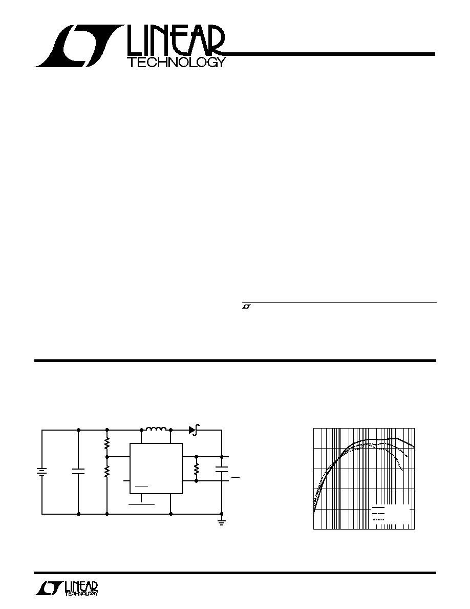
5V at 200mA from Two Cells
s
10
µ
A Quiescent Current in Shutdown
s
Operates with V
IN
as Low as 1.5V
s
Low-Battery Detector Active in Shutdown
s
Low Switch V
CESAT
: 370mV at 1A Typical
s
120
µ
A Quiescent Current in Active Mode
s
Switching Frequency Up to 300kHz
s
Programmable Peak Current with One Resistor
s
8-Lead SO Package
FEATURES
DESCRIPTIO
N
U
TYPICAL APPLICATIO
N
U
Efficiency
LOAD CURRENT (mA)
40
50
60
70
80
90
EFFICIENCY (%)
1304 TA02
0.1
1
10
500
100
V
IN
= 3.3V
V
IN
= 2.5V
V
IN
= 1.8V
V
IN
SW
SHDN
GND
SENSE
LBI
3
4
8
2
5
7
6
1
LBO
I
LIM
LT1304-5
+
+
100k
100
µ
F
NC
*
**
604k
100
µ
F
2 CELLS
499k
22
µ
H*
D1**
5V
200mA
LBO
LOW WHEN
V
BAT
< 2.2V
SUMIDA CD54-220
1N5817
1304 TA01
SHUTDOWN
2-Cell to 5V Step-Up Converter with Low-Battery Detect
2
LT1304/LT1304-3.3/LT1304-5
ABSOLUTE
M
AXI
M
U
M
RATINGS
W
W
W
U
PACKAGE/ORDER I
N
FOR
M
ATIO
N
W
U
U
V
IN
Voltage ................................................................ 8V
SW Voltage ............................................... 0.4V to 25V
FB Voltage (LT1304) ...................................... V
IN
+ 0.3V
Sense Voltage (LT1304-3.3/LT1304-5) ..................... 8V
I
LIM
Voltage .............................................................. 5V
SHDN Voltage ............................................................ 6V
LBI Voltage ............................................................... V
IN
LBO Voltage ............................................................... 8V
Maximum Power Dissipation ............................. 500mW
Junction Temperature .......................................... 125
°
C
Operating Temperature Range ..................... 0
°
C to 70
°
C
Storage Temperature Range ................. 65
°
C to 150
°
C
Lead Temperature (Soldering, 10 sec).................. 300
°
C
LT1304CS8
LT1304CS8-3.3
LT1304CS8-5
1304
13043
13045
S8 PART MARKING
ORDER PART
NUMBER
1
2
3
4
8
7
6
5
TOP VIEW
LBI
LBO
V
IN
SW
FB (SENSE)*
SHDN
I
LIM
GND
S8 PACKAGE
8-LEAD PLASTIC SO
*FIXED OUTPUT VERSION
T
JMAX
= 125
°
C,
JA
= 150
°
C/W
PARAMETER
CONDITIONS
MIN
TYP
MAX
UNITS
Minimum Operating Voltage
q
1.5
1.65
V
Operating Voltage Range
q
8
V
Quiescent Current
V
SHDN
= 2V, Not Switching
q
120
200
µ
A
Quiescent Current in Shutdown
V
SHDN
= 0V, V
IN
= 2V
q
7
15
µ
A
V
SHDN
= 0V, V
IN
= 5V
q
27
50
µ
A
Comparator Trip Point
LT1304
q
1.22
1.24
1.26
V
FB Pin Bias Current
LT1304
q
10
25
nA
Sense Pin Leakage in Shutdown
V
SHDN
= 0V, Fixed Output Versions
q
0.002
1
µ
A
Output Sense Voltage
LT1304-3.3
q
3.17
3.3
3.43
V
LT1304-5
q
4.80
5.05
5.25
V
Line Regulation
1.8V
V
IN
8V
q
0.04
0.15
%/V
LBI Input Threshold
Falling Edge
q
1.10
1.17
1.25
V
LBI Bias Current
q
6
20
nA
LBI Input Hysteresis
q
35
65
mV
LBO Output Voltage Low
I
SINK
= 500
µ
A
q
0.2
0.4
V
LBO Output Leakage Current
LBI = 1.5V, LBO = 5V
q
0.01
0.1
µ
A
SHDN Input Voltage High
q
1.4
V
SHDN Input Voltage Low
q
0.4
V
SHDN Pin Bias Current
V
SHDN
= 5V
q
5
8
µ
A
V
SHDN
= 0V
q
5
2
µ
A
Switch OFF Time
q
1
1.5
2
µ
s
Switch ON Time
Current Limit Not Asserted
q
4
6
8
µ
s
Maximum Duty Cycle
Current Limit Not Asserted
q
76
80
88
%
Peak Switch Current
I
LIM
Pin Open, V
IN
= 5V
0.8
1
1.2
A
20k from I
LIM
to GND
500
mA
V
IN
= 2V, V
SHDN
= 2V unless otherwise noted.
ELECTRICAL C
C
HARA TERISTICS
Consult factory for Industrial and Military grade parts.
3
LT1304/LT1304-3.3/LT1304-5
V
IN
= 2V, V
SHDN
= 2V unless otherwise noted.
ELECTRICAL C
C
HARA TERISTICS
The
q
denotes specifications which apply over the 0
°
C to 70
°
C operating
temperature range.
PARAMETER
CONDITIONS
MIN
TYP
MAX
UNITS
Switch Saturation Voltage
I
SW
= 1A
0.37
V
I
SW
= 700mA
q
0.26
0.35
V
Switch Leakage
Switch Off, V
SW
= 5V
q
0.01
7
µ
A
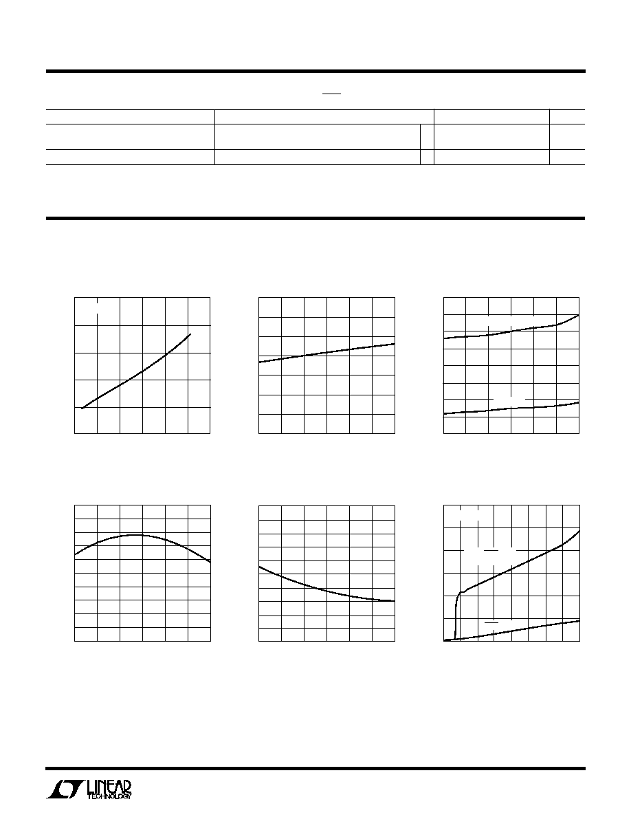
TYPICAL PERFOR
M
A
N
CE CHARACTERISTICS
U
W
TEMPERATURE (
°
C)
50
25
TIME (
µ
s)
0
50
25
75
100
1304 G03
8
7
6
5
4
3
2
1
0
MAXIMUM ON-TIME
OFF-TIME
On- and Off-Times
Supply Current
SWITCH CURRENT (A)
0
SATURATION VOLTAGE (mV)
500
400
300
200
100
0
0.2
0.4
0.6
0.8
1304 G01
1.0
1.2
T
A
= 25
°
C
TEMPERATURE (
°
C)
50
0
BIAS CURRENT (nA)
4
6
8
10
12
14
25
0
25
50
1304 G05
75
16
18
20
2
100
Feedback Pin Bias Current
Feedback Voltage
TEMPERATURE (
°
C)
50
FEEDBACK VOLTAGE (V)
1.250
1.245
1.240
1.235
1.230
1.225
1.220
1.215
1.210
1.205
1.200
25
0
25
50
1304 G04
75
100
TEMPERATURE (
°
C)
PEAK CURRENT (A)
1.3
1.2
1.1
1.0
0.9
0.8
0.7
0.6
1304 G02
50
25
0
25
50
75
100
Peak Switch Current Limit
Switch Saturation Voltage
INPUT VOLTAGE (V)
0
1
3
5
7
SUPPLY CURRENT (
µ
A)
2
4
6
8
1304 G06
300
250
200
150
100
50
0
V
SHDN
= V
IN
NOT SWITCHING
V
SHDN
= 0V
T
A
= 25
°
C
4
LT1304/LT1304-3.3/LT1304-5
TYPICAL PERFOR
M
A
N
CE CHARACTERISTICS
U
W
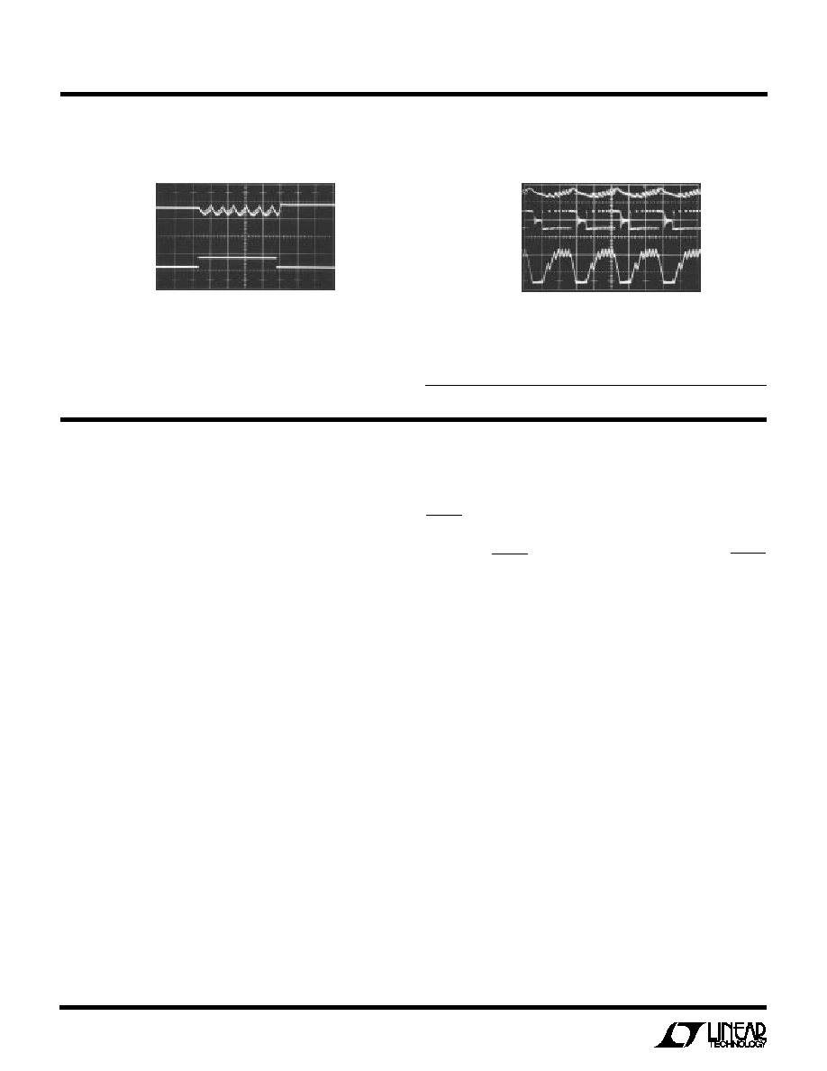
Load Transient Response
V
OUT
100mV/DIV
AC COUPLED
I
LOAD
200mA
0
V
SW
5V/DIV
100
µ
s/ DIV
1304 G07
20
µ
s/ DIV
1304 G08
V
OUT
100mV/DIV
AC COUPLED
Burst Mode
TM
Operation
I
L
500mA/DIV
V
IN
= 2.5V
V
OUT
= 5V
I
LOAD
= 185mA
L = 22
µ
H
PI
N
FU
N
CTIO
N
S
U
U
U
LBI (Pin 1): Low-Battery Detector Input. When voltage on
this pin is less than 1.17V, detector output is low.
LBO (Pin 2): Low-Battery Detector Output. Open collector
can sink up to 500
µ
A. Low-battery detector remains active
when device is shut down.
V
IN
(Pin 3): Input Supply. Must be bypassed close (< 0.2")
to the pin. See required layout in the Typical Applications.
SW (Pin 4): Collector of Power NPN. Keep copper traces on
this pin short and direct to minimize RFI.
GND (Pin 5): Device Ground. Must be low impedance;
solder directly to ground plane.
I
LIM
(Pin 6): Current Limit Set Pin. Float for 1A peak switch
current; a resistor to ground will lower peak current.
SHDN (Pin 7): Shutdown Input. When low, switching
regulator is turned off. The low-battery detector remains
active. The SHDN input should not be left floating. If SHDN
is not used, tie the pin to V
IN
.
FB/SENSE (Pin 8): On the LT1304 (adjustable) this pin
goes to the comparator input. On the fixed-output ver-
sions, the pin connects to the resistor divider which sets
output voltage. The divider is disconnected from the pin
during shutdown.
Burst Mode is a trademark of Linear Technology Corporation.
5
LT1304/LT1304-3.3/LT1304-5
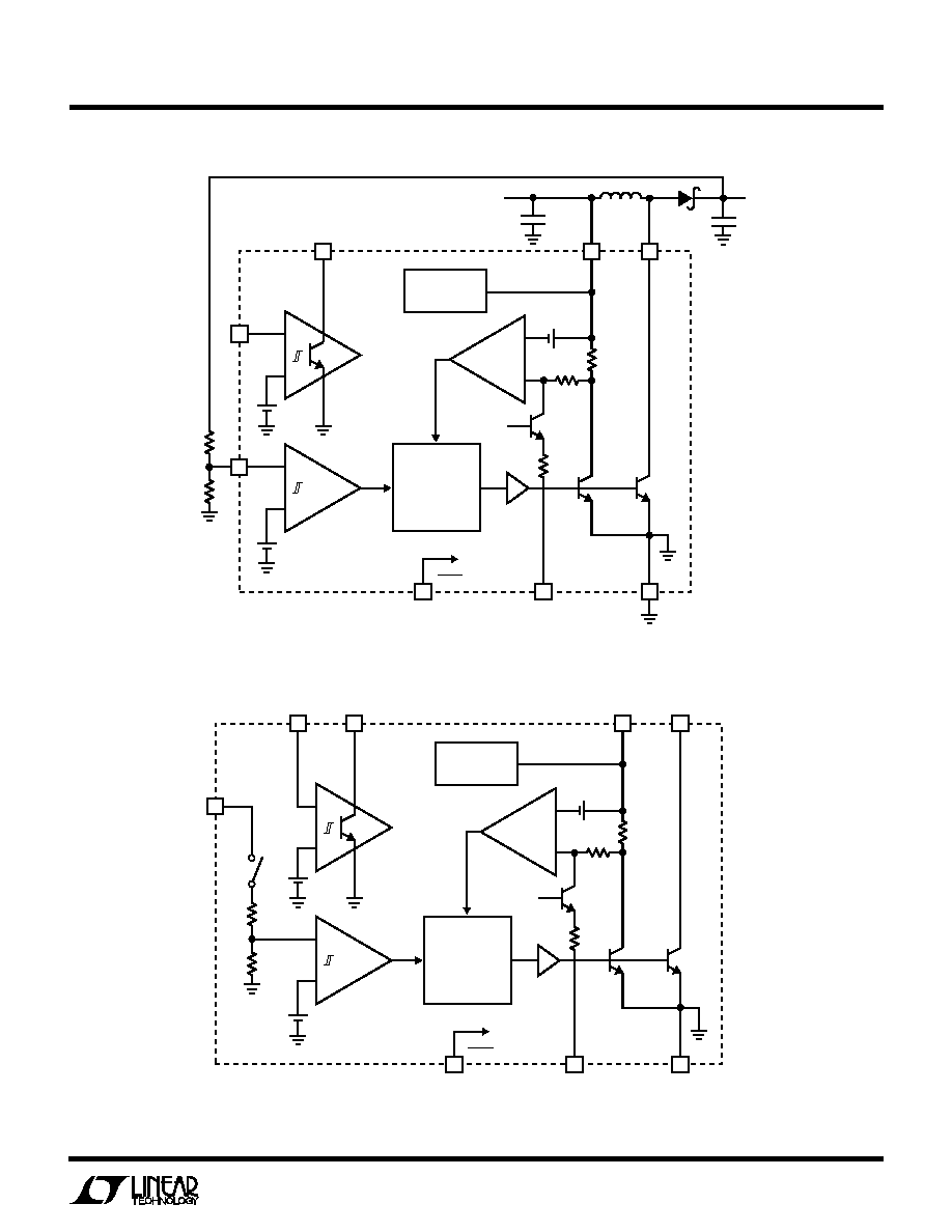
W
I
D AGRA
BLOCK
S
+
1304 F02
+
+
1.17V
R1
36mV
A3
OFF
LBI
SENSE
ENABLE
A2
LB0
SW
GND
I
LIM
SHDN
A1
8
6
5
4
V
IN
3
7
1
1.5V
UNDERVOLTAGE
LOCKOUT
Q3
Q2
×
1
Q1
×
200
R2
1k
590k
R1
7.2
1k
DRIVER
BIAS
~1V
2
1.24V
V
REF
SHUTDOWN
TIMERS
6
µ
s ON
1.5
µ
s OFF
R1 = 355k (LT1304-3.3), 195k (LT1304-5)
Figure 2. LT1304-3.3/LT1304-5 Block Diagram
+
1304 F01
+
+
1.17V
R4
36mV
A3
OFF
LBI
ENABLE
A2
LB0
C1
L1
SW
GND
I
LIM
SHDN
FB
A1
8
6
5
4
V
IN
V
OUT
V
IN
3
7
1
1.5V
UNDERVOLTAGE
LOCKOUT
Q3
Q2
×
1
Q1
×
200
R2
1k
R3
R1
7.2
1k
DRIVER
BIAS
~1V
2
1.24V
V
REF
SHUTDOWN
+
C2
D1
+
TIMERS
6
µ
s ON
1.5
µ
s OFF
Figure 1. LT1304 Block Diagram. Independent Low-Battery Detector A3 Remains Alive When Device Is in Shutdown