 | –≠–ª–µ–∫—Ç—Ä–æ–Ω–Ω—ã–π –∫–æ–º–ø–æ–Ω–µ–Ω—Ç: LT1307 | –°–∫–∞—á–∞—Ç—å:  PDF PDF  ZIP ZIP |
1
LT1307/LT1307B
Single Cell Micropower
600kHz PWM DC/DC Converters
DESCRIPTIO
N
U
FEATURES
The LT
Æ
1307/LT1307B are micropower, fixed frequency
DC/DC converters that operate from an input voltage as
low as 1V. First in the industry to achieve true current
mode PWM performance from a single cell supply, the
LT1307 features automatic shifting to power saving Burst
Mode operation at light loads. High efficiency is main-
tained over a broad 100
µ
A to 100mA load range. The
LT1307B does not shift into Burst Mode operation at light
loads, eliminating low frequency output ripple at the
expense of light load efficiency. The devices contain a low-
battery detector with a 200mV reference and shut down to
less than 5
µ
A. No load quiescent current of the LT1307 is
50
µ
A and the internal NPN power switch handles a 500mA
current with a voltage drop of just 295mV.
Unlike competitive devices, large electrolytic capacitors
are
not required with the LT1307/LT1307B in single cell
applications. The high frequency (600kHz) switching al-
lows the use of tiny surface mount multilayer ceramic
(MLC) capacitors along with small surface mount induc-
tors. The devices work with just 10
µ
F of output capaci-
tance and require only 1
µ
F of input bypassing.
The LT1307/LT1307B are available in 8-lead MSOP, PDIP
and SO packages.
s
Uses Small Ceramic Capacitors
s
50
µ
A Quiescent Current (LT1307)
s
1mA Quiescent Current (LT1307B)
s
Operates with V
IN
as Low as 1V
s
600kHz Fixed Frequency Operation
s
Starts into Full Load
s
Low Shutdown Current: 3
µ
A
s
Low-Battery Detector
s
3.3V at 75mA from a Single Cell
s
Automatic Burst Mode
TM
Operation at
Light Load (LT1307)
s
Continuous Switching at Light Load (LT1307B)
s
Low V
CESAT
Switch: 295mV at 500mA
s
Pagers
s
Cordless Telephones
s
GPS Receivers
s
Battery Backup
s
Portable Electronic Equipment
s
Glucose Meters
s
Diagnostic Medical Instrumentation
APPLICATIO
N
S
U
Burst Mode is a trademark of Linear Technology Corporation.
, LTC and LT are registered trademarks of Linear Technology Corporation.
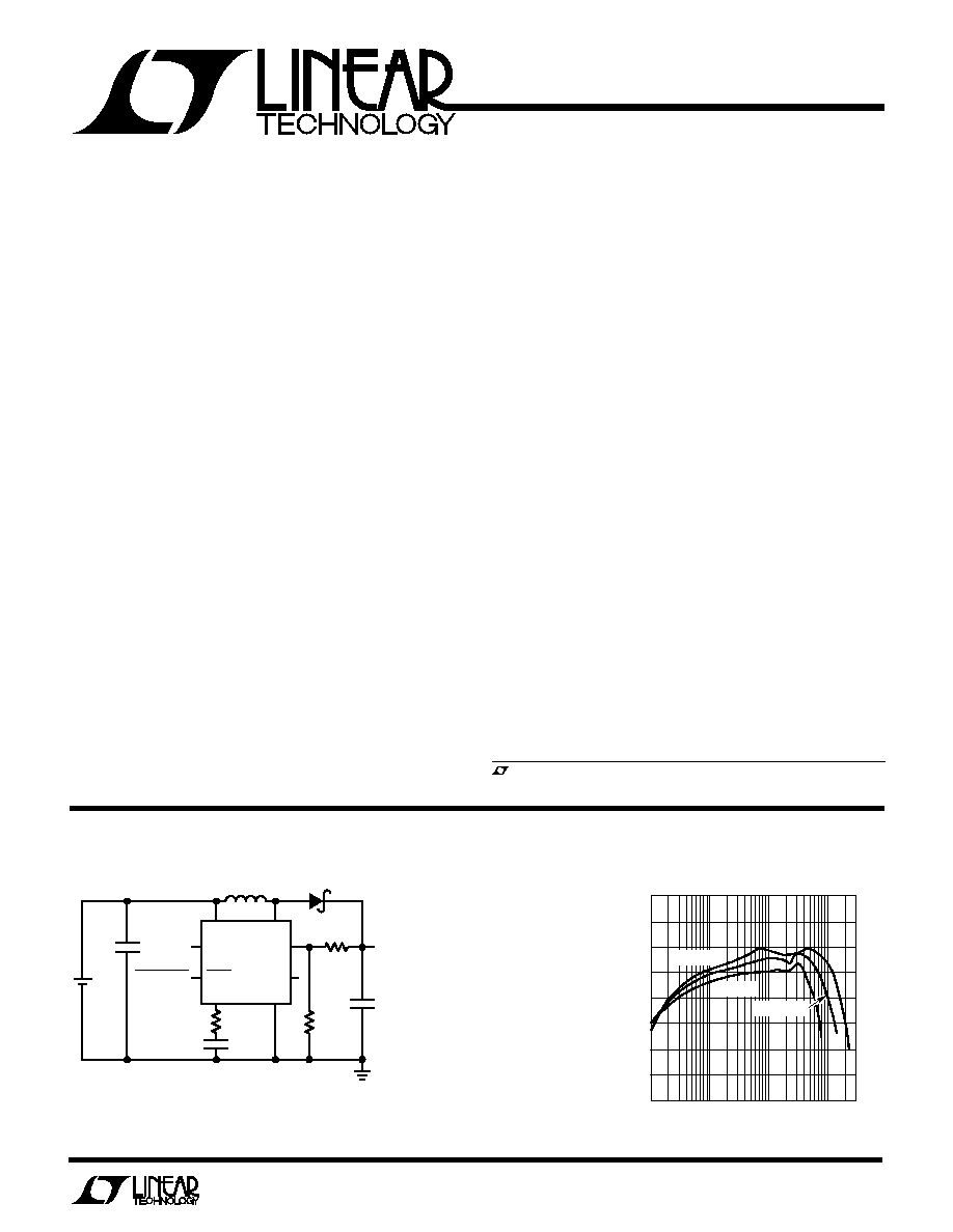
TYPICAL APPLICATIO
N
U
Single Cell to 3.3V Converter Efficiency
LOAD CURRENT (mA)
0.1
70
EFFICIENCY (%)
80
90
1
10
100
1307 TA01
60
50
V
IN
= 1.5V
V
IN
= 1V
V
IN
= 1.25V
V
IN
SW
FB
LT1307
L1
10
µ
H
D1
LBO
LBI
SHDN
SHUTDOWN
100k
R2
604k
1%
3.3V
75mA
R1
1.02M
1%
680pF
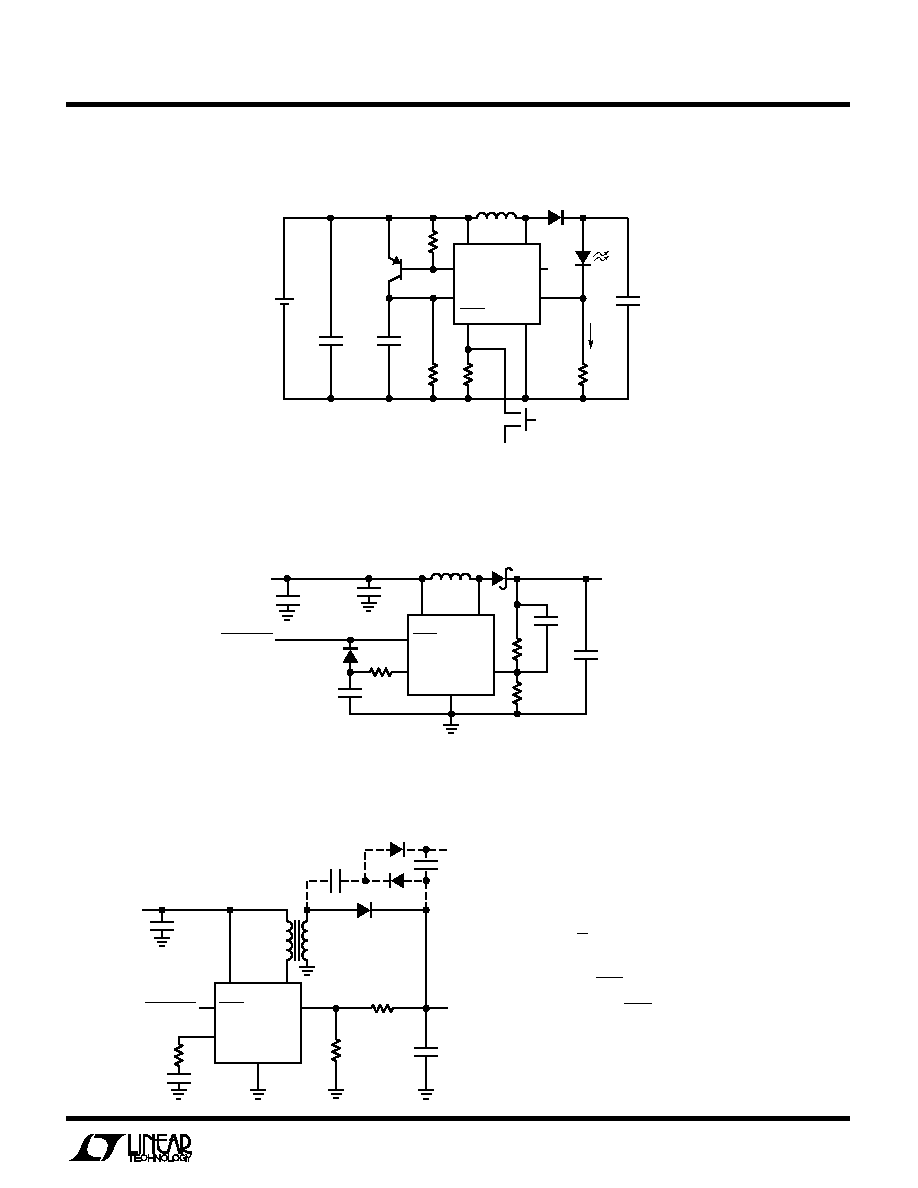
FOR 5V OUTPUT: R1 = 1M, R2 = 329k
C1: MURATA-ERIE GRM235Y5V105Z01
MARCON THCS50E1E105Z
TOKIN 1E105ZY5U-C103-F
C2: MURATA-ERIE GRM235Y5V106Z01
MARCON THCS50E1E105Z
TOKIN 1E106ZY5U-C304-F
1307 F01
C1
1
µ
F
C2
10
µ
F
1.5V
CELL
V
C
GND
D1: MOTOROLA MBR0520L
L1: COILCRAFT D01608C-103
SUMIDA CD43-100
MURATA ERIE LQH3C100
Figure 1. Single Cell to 3.3V Boost Converter
2
LT1307/LT1307B
A
U
G
W
A
W
U
W
A
R
BSOLUTE
XI
TI
S
V
IN
, SHDN, LBO Voltage ......................................... 12V
SW Voltage ............................................................. 30V
FB Voltage ....................................................... V
IN
+ 1V
V
C
Voltage ................................................................ 2V
LBI Voltage ............................................ 0V
V
LBI
1V
Current into FB Pin ..............................................
±
1mA
Junction Temperature ........................................... 125
∞
C
Operating Temperature Range
Commercial (Note 1) ......................... ≠ 20
∞
C to 70
∞
C
Industrial ........................................... ≠ 40
∞
C to 85
∞
C
Storage Temperature Range ................ ≠ 65
∞
C to 150
∞
C
Lead Temperature (Soldering, 10 sec)................. 300
∞
C
W
U
U
PACKAGE/ORDER I FOR ATIO
T
JMAX
= 125
∞
C,
JA
= 160
∞
C/W
ORDER PART
NUMBER
ORDER PART
NUMBER
1
2
3
4
V
C
FB
SHDN
GND
8
7
6
5
LBO
LBI
V
IN
SW
TOP VIEW
MS8 PACKAGE
8-LEAD PLASTIC MSOP
1
2
3
4
8
7
6
5
TOP VIEW
LBO
LBI
V
IN
SW
V
C
FB
SHDN
GND
N8 PACKAGE
8-LEAD PDIP
S8 PACKAGE
8-LEAD PLASTIC SO
LT1307CMS8
LT1307BCMS8
LT1307CN8
LT1307CS8
LT1307IS8
LT1307BCS8
LT1307BIS8
T
JMAX
= 125
∞
C,
JA
= 100
∞
C/W (N8)
T
JMAX
= 125
∞
C,
JA
= 120
∞
C/W (S8)
S8 PART MARKING
1307
1307B
1307I
1307BI
MS8 PART MARKING
Consult factory for Military grade parts.
Commercial Grade 0
∞
C to 70
∞
C. V
IN
= 1.1V, V
SHDN
= V
IN
, T
A
= 25
∞
C, LT1307/LT1307B unless otherwise noted.
ELECTRICAL C
C
HARA TERISTICS
SYMBOL
PARAMETER
CONDITIONS
MIN
TYP
MAX
UNITS
I
Q
Quiescent Current
Not Switching (LT1307)
q
50
90
µ
A
Not Switching (LT1307B)
q
1.0
1.5
mA
V
SHDN
= 0V
q
1
3
µ
A
V
FB
Feedback Voltage
q
1.20
1.22
1.24
V
I
B
FB Pin Bias Current (Note 2)
V
FB
= V
REF
q
27
60
nA
Reference Line Regulation
1V
V
IN
2V (25
∞
C, 0
∞
C)
0.6
1.1
%/V
1V
V
IN
2V (70
∞
C)
1.5
%/V
2V
V
IN
5V
q
0.3
0.8
%/V
Minimum Input Voltage
0.92
1
V
Input Voltage Range
q
1
5
V
g
m
Error Amp Transconductance
I = 5
µ
A
q
25
35
65
µ
mhos
A
V
Error Amp Voltage Gain
25
∞
C, 0
∞
C
35
100
V/V
70
∞
C
30
V/V
f
OSC
Switching Frequency
q
550
600
750
kHz
BU
BF
3
LT1307/LT1307B
SYMBOL
PARAMETER
CONDITIONS
MIN
TYP
MAX
UNITS
Maximum Duty Cycle
25
∞
C, 0
∞
C
80
84
%
70
∞
C
76
%
Switch Current Limit (Note 3)
DC = 40%
q
0.6
1.25
A
DC = 75%
0.5
A
Switch V
CESAT
I
SW
= 500mA (25
∞
C, 0
∞
C)
295
350
mV
I
SW
= 500mA (70
∞
C)
400
mV
Burst Mode Operation Switch Current Limit
L = 10
µ
H
100
mA
(LT1307 Only)
L = 22
µ
H
50
mA
Shutdown Pin Current
V
SHDN
= V
IN
q
2.5
4.0
µ
A
V
SHDN
= 0V
q
≠ 1.5
≠ 2.5
µ
A
LBI Threshold Voltage
q
190
200
210
mV
LBO Output Low
I
SINK
= 10
µ
A
q
0.1
0.25
V
LBO Leakage Current
V
LBI
= 250mV, V
LBO
= 5V
q
0.01
0.1
µ
A
LBI Input Bias Current (Note 4)
V
LBI
= 150mV
q
5
25
nA
Low-Battery Detector Gain
1M
Load (25
∞
C, 0
∞
C)
1000
3000
V/V
1M
Load (70
∞
C)
500
V/V
Switch Leakage Current
V
SW
= 5V
q
0.01
3
µ
A
Reverse Battery Current
(Note 5)
750
mA
Commercial Grade 0
∞
C to 70
∞
C. V
IN
= 1.1V, V
SHDN
= V
IN
, T
A
= 25
∞
C unless otherwise noted.
ELECTRICAL C
C
HARA TERISTICS
Commercial Grade T
A
= ≠ 20
∞
C, V
IN
= 1.1V, V
SHDN
= V
IN
, unless otherwise noted (Note 1).
SYMBOL
PARAMETER
CONDITIONS
MIN
TYP
MAX
UNITS
I
Q
Quiescent Current
V
FB
= 1.3V, Not Switching (LT1307)
50
100
µ
A
V
FB
= 1.3V, Not Switching (LT1307B)
1.1
1.6
mA
V
SHDN
= 0V
1
3
µ
A
V
FB
Feedback Voltage
1.195
1.22
1.245
V
g
m
Error Amp Transconductance
I = 5
µ
A
25
35
65
µ
mhos
A
V
Error Amp Voltage Gain
35
100
V/V
f
OSC
Switching Frequency
500
600
750
kHz
Maximum Duty Cycle
80
84
%
Switch V
CESAT
I
SW
= 500mA, V
IN
= 1.2V
250
350
mV
Shutdown Pin Current
V
SHDN
= V
IN
2.5
4.0
µ
A
V
SHDN
= 0V
≠ 1.5
≠ 2.5
µ
A
LBI Threshold Voltage
186
200
210
mV
4
LT1307/LT1307B
ELECTRICAL C
C
HARA TERISTICS
Industrial Grade ≠ 40
∞
C to 85
∞
C. V
IN
= 1.1V, V
SHDN
= V
IN
, LT1307/LT1307B unless otherwise noted.
SYMBOL
PARAMETER
CONDITIONS
MIN
TYP
MAX
UNITS
I
Q
Quiescent Current
V
FB
= 1.3V, Not Switching (LT1307)
q
50
100
µ
A
V
FB
= 1.3V, Not Switching (LT1307B)
q
1
1.8
mA
V
SHDN
= 0V
q
1
3
µ
A
V
FB
Feedback Voltage
q
1.195
1.22
1.245
V
I
B
FB Pin Bias Current (Note 2)
V
FB
= V
REF
q
10
27
100
nA
Reference Line Regulation
1V
V
IN
2V (≠ 40
∞
C)
0.6
1.1
%/V
1V
V
IN
2V (85
∞
C)
3.2
%/V
2V
V
IN
5V
q
0.3
0.8
%/V
Minimum Input Voltage
≠ 40
∞
C
1.1
1.2
V
85
∞
C
0.8
1.0
V
Input Voltage Range
q
5
V
g
m
Error Amp Transconductance
I = 5
µ
A
q
25
35
65
µ
mhos
A
V
Error Amp Voltage Gain
≠ 40
∞
C
35
V/V
85
∞
C
30
V/V
f
OSC
Switching Frequency
q
500
600
750
kHz
Maximum Duty Cycle
≠ 40
∞
C
80
84
%
85
∞
C
75
80
%
Switch Current Limit (Note 3)
DC = 40%
q
0.6
1.25
A
DC = 75%
0.5
A
Switch V
CESAT
I
SW
= 500mA, V
IN
= 1.2V (≠ 40
∞
C)
250
350
mV
I
SW
= 500mA (85
∞
C)
330
400
mV
Burst Mode Operation Switch Current Limit
L = 10
µ
H
100
mA
(LT1307 Only)
L = 22
µ
H
50
mA
Shutdown Pin Current
V
SHDN
= V
IN
q
2.5
4.0
µ
A
V
SHDN
= 0V
q
≠ 1.5
≠ 2.5
µ
A
LBI Threshold Voltage
q
186
200
210
mV
LBO Output Low
I
SINK
= 10
µ
A
q
0.1
0.25
V
LBO Leakage Current
V
LBI
= 250mV, V
LBO
= 5V
q
0.1
0.3
µ
A
LBI Input Bias Current (Note 4)
V
LBI
= 150mV
q
5
30
nA
Low-Battery Detector Gain
1M
Load (≠ 40
∞
C)
1000
6000
V/V
1M
Load (85
∞
C)
400
V/V
Switch Leakage Current
V
SW
= 5V
q
0.01
3
µ
A
Note 2: Bias current flows into FB pin.
Note 3: Switch current limit guaranteed by design and/or correlation to
static tests. Duty cycle affects current limit due to ramp generator.
Note 4: Bias current flows out of LBI pin.
Note 5: The LT1307 will withstand continuous application of 1.6V applied
to the GND pin while V
IN
and SW are grounded.
The
q
denotes specifications which apply over the full operating
temperature range.
Note 1: Specifications for commercial (C) grade devices are guaranteed
but not tested at ≠ 20
∞
C. MS8 package devices are designed for and
intended to meet commercial temperature range specifications but are not
tested at ≠ 20
∞
C or 0
∞
C.
5
LT1307/LT1307B
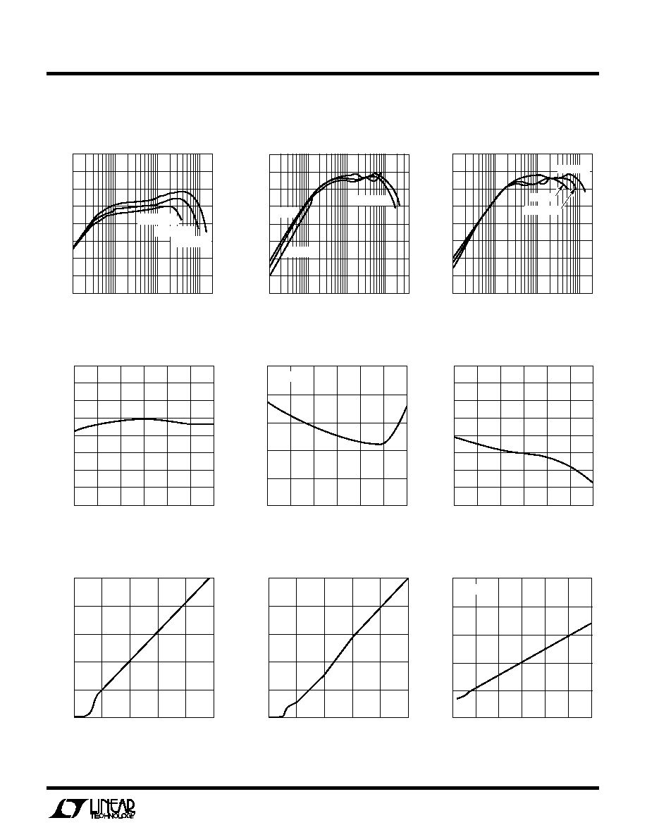
TYPICAL PERFOR
M
A
N
CE CHARACTERISTICS
U
W
LOAD CURRENT (mA)
50
60
70
80
90
EFFICIENCY (%)
200
0.1
1
10
100
LT1307 ∑ G01
V
IN
= 1.00V
V
IN
= 1.25V
V
IN
= 1.5V
3.3V Output Efficiency, Circuit of
Figure 1 (LT1307B)
5V Output Efficiency, Circuit of
Figure 1 (LT1307B)
LOAD CURRENT (mA)
0.1
EFFICIENCY (%)
90
80
70
60
50
40
30
20
10
1
10
LT1307 ∑ TPC03
100
V
IN
= 1V
V
IN
= 1.5V
V
IN
= 1.25V
Quiescent Current vs Temperature
Feedback Bias Current vs
Temperature
LBI Bias Current vs Temperature
5V Output Efficiency, Circuit of
Figure 1 (LT1307)
TEMPERATURE (
∞
C)
≠50
QUIESCENT CURRENT (
µ
A)
25
75
LT1307 ∑ TPC04
≠25
0
50
80
70
60
50
40
30
20
10
0
100
TEMPERATURE (
∞
C)
≠50
0
FEEDBACK BIAS CURRENT (nA)
10
20
30
40
50
≠25
0
25
50
LTC1307 ∑ TPC05
75
100
V
IN
= 1.1V
TEMPERATURE (
∞
C)
≠50
LBI BIAS CURRENT (nA)
25
75
LT1307 ∑ TPC06
≠25
0
50
16
14
12
10
8
6
4
2
0
100
Quiescent Current in Shutdown
Shutdown Pin Bias Current vs
Input Voltage
Switch V
CESAT
vs Current
INPUT VOLTAGE (V)
0
QUIESCENT CURRENT (
µ
A)
10
8
6
4
2
0
4
LT1307 ∑ TPC07
1
2
3
5
INPUT VOLTAGE (V)
0
SHUTDOWN PIN CURRENT (
µ
A)
10
16
12
8
4
0
4
LT1307 ∑ TPC08
1
2
3
5
SWITCH CURRENT (mA)
0
0
V
CESAT
(mV)
100
200
300
400
500
100
200
300
400
LT1307 ∑ TPC09
500
600
T
A
= 25
∞
C
LOAD CURRENT (mA)
0.1
50
EFFICIENCY (%)
70
90
100
10
1
1307 G02
30
40
60
80
20
10
V
IN
= 1.25V
V
IN
= 1.5V
V
IN
= 1V
6
LT1307/LT1307B
TYPICAL PERFOR
M
A
N
CE CHARACTERISTICS
U
W
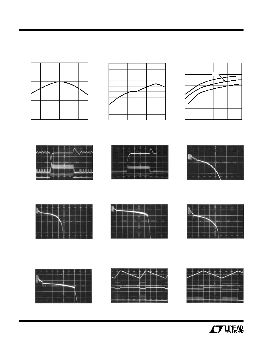
Feedback Voltage vs
Temperature
LBI Reference vs Temperature
Oscillator Frequency vs
Input Voltage
TEMPERATURE (
∞
C)
≠50
FEEDBACK VOLTAGE (V)
1.230
1.225
1.220
1.215
1.210
1.205
1.200
≠25
0
25
50
LT1307 ∑ TPC10
75
100
V
IN
= 1.25V
500
µ
s/DIV
1307 G13
V
OUT
= 3.3V
Transient Response (LT1307)
I
L
200mA/DIV
V
OUT
200mV/DIV
AC COUPLED
55mA
5mA
I
LOAD
V
IN
= 0.92V
I
LOAD
10mA/DIV
1307 G15
V
OUT
= 3.3V
Load Regulation (LT1307)
V
OUT
50mV/DIV
DC
COUPLED
OFFSET
ADDED
TEMPERATURE (
∞
C)
≠50
REFERENCE VOLTAGE (mV)
≠25
0
25
50
LT1307 ∑ TPC11
75
210
208
206
204
202
200
198
196
194
192
190
100
V
IN
= 1.25V
500
µ
s/DIV
1307 G14
V
OUT
= 3.3V
Transient Response (LT1307B)
I
L
200mA/DIV
V
OUT
200mV/DIV
AC COUPLED
55mA
5mA
V
IN
= 1.15V
I
LOAD
20mA/DIV
1307 G17
V
OUT
= 3.3V
Load Regulation (LT1307)
V
IN
= 1V
I
LOAD
10mA/DIV
1307 G18
V
OUT
= 5V
Load Regulation (LT1307)
V
OUT
50mV/DIV
DC
COUPLED
OFFSET
ADDED
V
OUT
50mV/DIV
DC
COUPLED
OFFSET
ADDED
V
IN
= 1V
I
LOAD
20mA/DIV
1307 G16
V
OUT
= 3.3V
Load Regulation (LT1307)
V
OUT
50mV/DIV
DC
COUPLED
OFFSET
ADDED
Load Regulation (LT1307)
I
LOAD
V
IN
= 1.25V
100
µ
s/DIV
1307 G21
V
OUT
= 5V
I
LOAD
= 1.5mA
I
L
100mA/DIV
V
SW
5V/DIV
V
OUT
50mV/DIV
AC COUPLED
V
OUT
50mV/DIV
AC COUPLED
V
IN
= 1.25V
100
µ
s/DIV
1307 G20
V
OUT
= 5V
I
LOAD
= 1.5mA
I
L
100mA/DIV
V
SW
5V/DIV
V
OUT
50mV/DIV
DC
COUPLED
OFFSET
ADDED
V
IN
= 1.15V
I
LOAD
10mA/DIV
1307 G19
V
OUT
= 5V
Circuit Operation, L = 22
µ
H
(LT1307)
Circuit Operation, L = 10
µ
H
(LT1307)
INPUT VOLTAGE (V)
1
FREQUENCY (kHz)
600
700
5
LT1307 ∑ TPC12
500
400
2
3
4
900
800
85
∞
C
≠40
∞
C
25
∞
C
7
LT1307/LT1307B
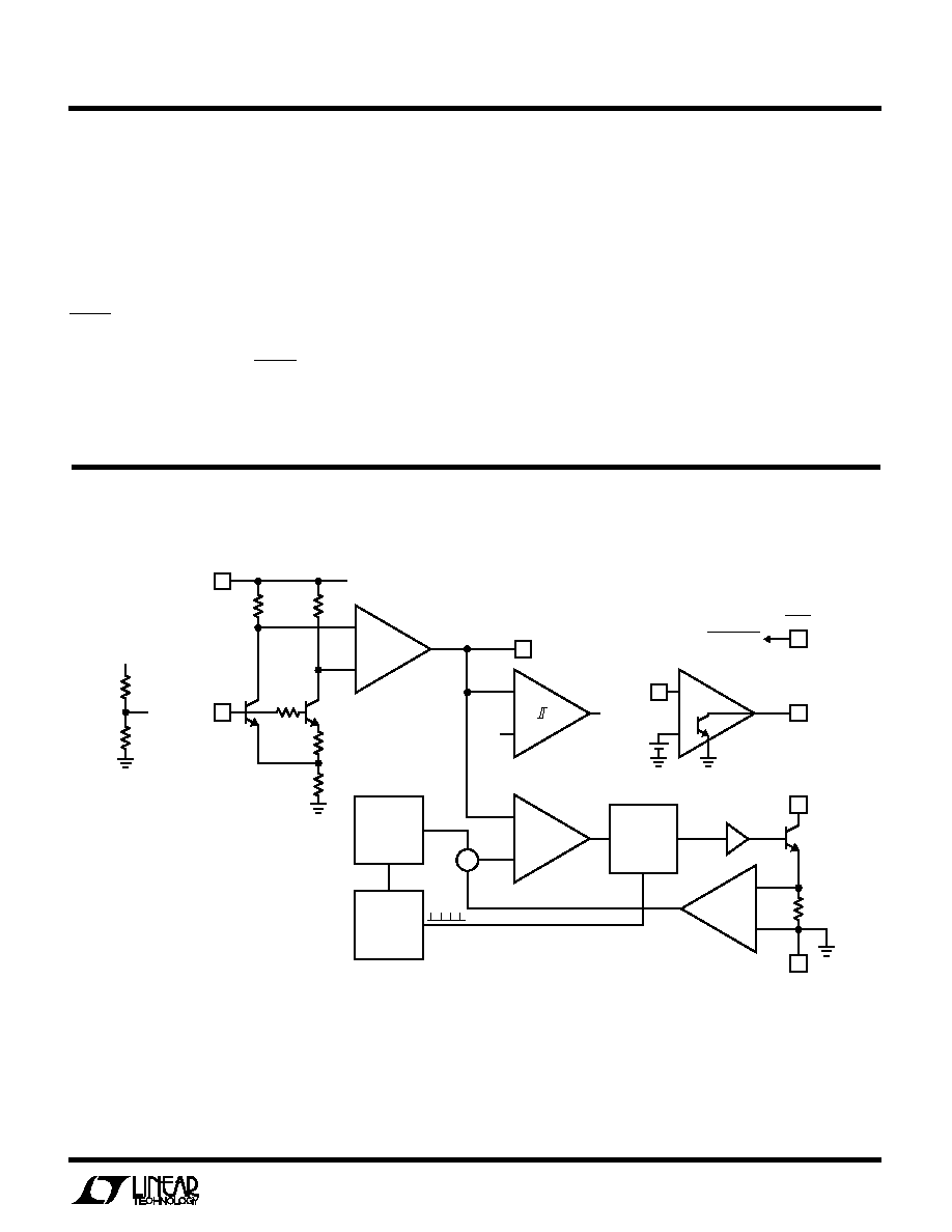
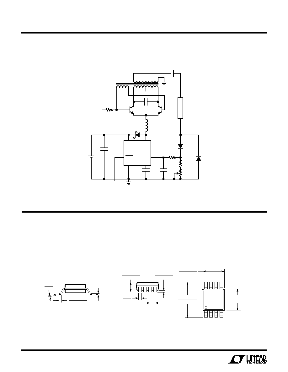
BLOCK DIAGRA
M
W
V
C
(Pin 1): Compensation Pin for Error Amplifier. Con-
nect a series RC from this pin to ground. Typical values
are 100k
and 680pF. Minimize trace area at V
C
.
FB (Pin 2): Feedback Pin. Reference voltage is 1.22V.
Connect resistor divider tap here. Minimize trace area at
FB. Set V
OUT
according to: V
OUT
= 1.22V(1 + R1/R2).
SHDN (Pin 3): Shutdown. Ground this pin to turn off
switcher. Must be tied to V
IN
(or higher voltage) to enable
switcher. Do not float the SHDN pin.
GND (Pin 4): Ground. Connect directly to local ground
plane.
PI
N
FU
N
CTIO
N
S
U
U
U
SW (Pin 5): Switch Pin. Connect inductor/diode here.
Minimize trace area at this pin to keep EMI down.
V
IN
(Pin 6): Supply Pin. Must have 1
µ
F ceramic bypass
capacitor right at the pin, connected directly to ground.
LBI (Pin 7): Low-Battery Detector Input. 200mV refer-
ence. Voltage on LBI must stay between ground and
700mV.
LBO (Pin 8): Low-Battery Detector Output. Open collec-
tor, can sink 10
µ
A. A 1M
pull-up is recommended.
Figure 2. LT1307/LT1307B Block Diagram
≠
+
≠
+
≠
+
≠
+
≠
+
+
+
COMPARATOR
RAMP
GENERATOR
R
BIAS
V
C
g
m
Q2
◊
10
Q1
FB
FB
ENABLE
200mV
A = 3
FF
A2
A1
ERROR
AMPLIFIER
A4
0.15
DRIVER
SW
GND
1307 F02
Q3
Q
S
600kHz
OSCILLATOR
5
LBO
LBI
SHDN
SHUTDOWN
3
7
1
4
R6
40k
R5
40k
R1
(EXTERNAL)
R3
30k
R4
140k
2
V
IN
V
IN
V
OUT
6
8
R2
(EXTERNAL)
*HYSTERESIS IN LT1307 ONLY
*
8
LT1307/LT1307B
APPLICATIO
N
S I
N
FOR
M
ATIO
N
W
U
U
U
OPERATION
The LT1307 combines a current mode, fixed frequency
PWM architecture with Burst Mode micropower operation
to maintain high efficiency at light loads. Operation can
best be understood by referring to the block diagram in
Figure 2. Q1 and Q2 form a bandgap reference core whose
loop is closed around the output of the converter. When
V
IN
is 1V, the feedback voltage of 1.22V, along with an
80mV drop across R5 and R6, forward biases Q1 and Q2's
base collector junctions to 300mV. Because this is not
enough to saturate either transistor, FB can be at a higher
voltage than V
IN
. When there is no load, FB rises slightly
above 1.22V, causing V
C
(the error amplifier's output) to
decrease. When V
C
reaches the bias voltage on hysteretic
comparator A1, A1's output goes low, turning off all
circuitry except the input stage, error amplifier and low-
battery detector. Total current consumption in this state is
50
µ
A. As output loading causes the FB voltage to de-
crease, A1's output goes high, enabling the rest of the IC.
Switch current is limited to approximately 100mA initially
after A1's output goes high. If the load is light, the output
voltage (and FB voltage) will increase until A1's output
goes low, turning off the rest of the LT1307. Low fre-
quency ripple voltage appears at the output. The ripple
frequency is dependent on load current and output capaci-
tance. This Burst Mode operation keeps the output regu-
lated and reduces average current into the IC, resulting in
high efficiency even at load currents of 100
µ
A or less.
If the output load increases sufficiently, A1's output re-
mains high, resulting in continuous operation. When the
LT1307 is running continuously, peak switch current is
controlled by V
C
to regulate the output voltage. The switch
is turned on at the beginning of each switch cycle. When
the summation of a signal representing switch current and
a ramp generator (introduced to avoid subharmonic oscil-
lations at duty factors greater than 50%) exceeds the V
C
signal, comparator A2 changes state, resetting the flip-
flop and turning off the switch. Output voltage increases as
switch current is increased. The output, attenuated by a
resistor divider, appears at the FB pin, closing the overall
loop. Frequency compensation is provided by an external
series RC network connected between the V
C
pin and
ground. Low-battery detector A4's open collector output
(LBO) pulls low when the LBI pin voltage drops below
200mV. There is no hysteresis in A4, allowing it to be used
as an amplifier in some applications. The entire device is
disabled when the SHDN pin is brought low. To enable the
converter, SHDN must be at V
IN
or at a higher voltage.
The LT1307B differs from the LT1307 in that there is no
hysteresis in comparator A1. Also, the bias point on A1 is
set lower than on the LT1307 so that switching can occur
at inductor current less than 100mA. Because A1 has no
hysteresis, there is no Burst Mode operation at light loads
and the device continues switching at constant frequency.
This results in the absence of low frequency output voltage
ripple at the expense of efficiency.
The difference between the two devices is clearly illus-
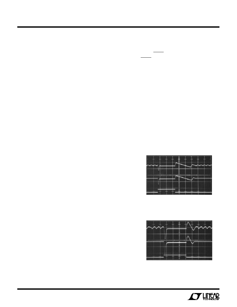
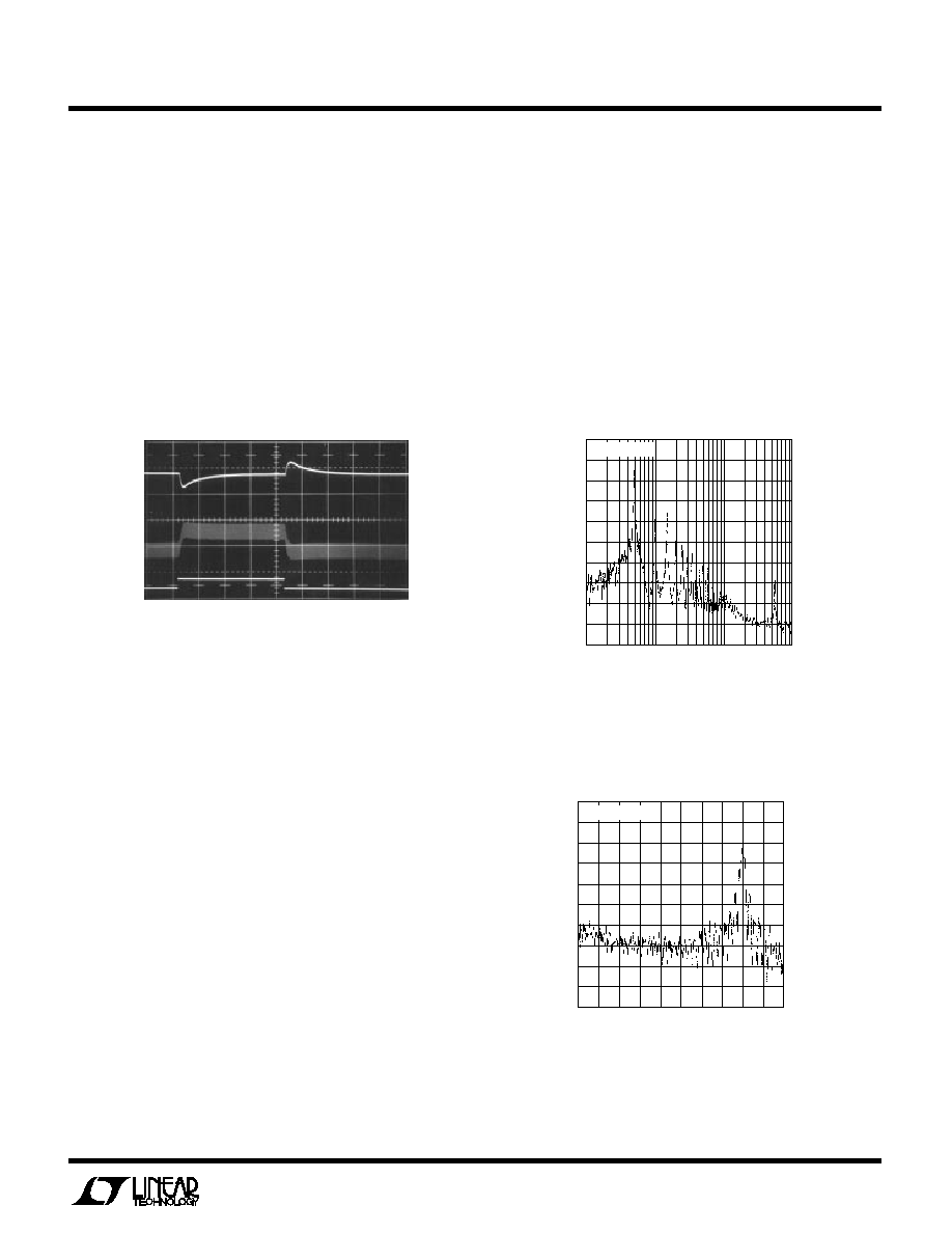
trated in Figures 3 and 4. The top two traces in Figure 3
show an LT1307/LT1307B circuit, using the components
indicated in Figure 1, set to a 5V output. Input voltage is
1.25V. Load current is stepped from 1mA to 41mA for both
circuits. Low frequency Burst Mode operation voltage
ripple is observed on Trace A, while none is observed on
TRACE A
TRACE B
LT1307
V
OUT
500mV/DIV
AC COUPLED
41mA
1mA
I
L
LT1307B
V
OUT
500mV/DIV
AC COUPLED
V
IN
= 1.25V
1ms/DIV
1307 F03
V
OUT
= 5V
Figure 3. LT1307 Exhibits Burst Mode Operation Ripple at
1mA Load, LT1307B Does Not
LT1307
V
OUT
200mV/DIV
AC COUPLED
TRACE A
45mA
5mA
I
L
LT1307B
V
OUT
200mV/DIV
AC COUPLED
TRACE B
V
IN
= 1.5V
500
µ
s/DIV
1307 F04
V
OUT
= 5V
Figure 4. At Higher Loading and a 1.5V Supply, LT1307
Again Exhibits Burst Mode Operation Ripple at 5mA Load,
LT1307B Does Not
9
LT1307/LT1307B
APPLICATIO
N
S I
N
FOR
M
ATIO
N
W
U
U
U
quite evident, as is this particular device's 575kHz switch-
ing frequency (nominal switching frequency is 600kHz).
Note, however, the absence of significant energy at 455kHz.
Figure 7's plot reduces the frequency span from 255kHz to
655kHz with a 455kHz center. Burst Mode low frequency
ripple creates sidebands around the 575kHz switching
fundamental. These sidebands have low signal amplitude
at 455kHz, measuring ≠ 55dBmV
RMS
. As load current is
further reduced, the Burst Mode frequency decreases.
This spaces the sidebands around the switching fre-
quency closer together, moving spectral energy further
Trace B. Similarly, Figure 4 details the two circuits with a
load step from 5mA to 45mA with a 1.5V input.
The LT1307B also can be used in lower current applica-
tions where a clean, low ripple output is needed. Figure 5
details transient response of a single cell to 3.3V con-
verter, using an inductor value of 100
µ
H. This high induc-
tance minimizes ripple current, allowing the LT1307B to
regulate without skipping cycles. As the load current is
stepped from 5mA to 10mA, the output voltage responds
cleanly. Note that the V
C
pin loop compensation has been
made more conservative (increased C, decreased R).
Figure 5. Increasing L to 100
µ
H, Along with R
C
= 36k,
C
C
= 20nF and C
OUT
= 10
µ
F, Low Noise Performance of
LT1307B Can Be Realized at Light Loads of 5mA to 10mA
10mA
5mA
I
L
V
IN
= 1.25V
1ms/DIV
1307 F05
V
OUT
= 3.3V
I
L
20mA/DIV
V
OUT
100mV/DIV
AC COUPLED
At light loads, the LT1307B will begin to skip alternate
cycles. The load point at which this occurs can be de-
creased by increasing the inductor value. However, output
ripple will continue to be significantly less than the LT1307
output ripple. Further, the LT1307B can be forced into
micropower mode, where I
Q
falls from 1mA to 50
µ
A by
pulling down V
C
to 0.3V or less externally.
DC/DC CONVERTER NOISE CONSIDERATIONS
Switching regulator noise is a significant concern in many
communications systems. The LT1307 is designed to
keep noise energy out of the sensitive 455kHz band at all
load levels while consuming only 60
µ
W to 100
µ
W at no
load. At light load levels, the device is in Burst Mode,
causing low frequency ripple to appear at the output.
Figure 6 details spectral noise directly at the output of
Figure 1's circuit in a 1kHz to 1MHz bandwidth. The
converter supplies a 5mA load from a 1.25V input. The
Burst Mode fundamental at 5.1kHz and its harmonics are
FREQUENCY (kHz)
1
OUTPUT NOISE VOLTAGE (dBmV
RMS
)
40
30
20
10
0
≠10
≠20
≠30
≠40
≠50
≠60
10
100
1000
1307 F06
RBW = 100Hz
Figure 6. Spectral Noise Plot of 3.3V Converter Delivering
5mA Load. Burst Mode Fundamental at 5.1kHz is 23dBmV
RMS
or 14mV
RMS
FREQUENCY (kHz)
255
OUTPUT NOISE VOLTAGE (dBmV
RMS
)
≠20
≠25
≠30
≠35
≠40
≠45
≠50
≠55
≠60
≠65
≠70
455
1307 F07
655
RBW = 100Hz
Figure 7. Span Centered at 455kHz Shows ≠ 55dBmV
RMS
(1.8
µ
V
RMS
) at 455kHz. Burst Mode Creates Sidebands 5.1kHz
Apart Around the Switching Frequency Fundamental of 575kHz
10
LT1307/LT1307B
APPLICATIO
N
S I
N
FOR
M
ATIO
N
W
U
U
U
To eliminate the low frequency noise of Figure 6, the
LT1307 can be replaced with the LT1307B. Figure 9
details the spectral noise at the output of Figure 1's circuit
using an LT1307B at 5mA load. Although spectral energy
is present at 333kHz due to alternate pulse skipping, all
Burst Mode operation spectral components are gone.
Alternate pulse skipping can be eliminated by increasing
inductance.
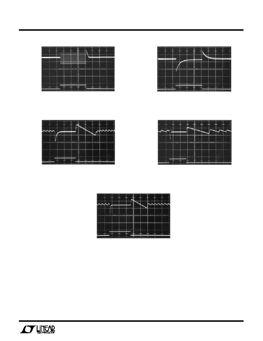
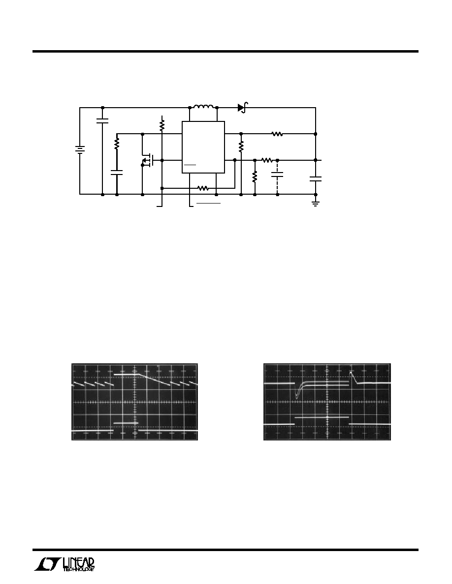
FREQUENCY COMPENSATION
Obtaining proper values for the frequency compensation
network is largely an empirical, iterative procedure, since
variations in input and output voltage, topology, capacitor
value and ESR, and inductance make a simple formula
elusive. As an example, consider the case of a 1.25V to
3.3V boost converter supplying 50mA. To determine
optimum compensation, the circuit is built and a transient
load is applied to the circuit. Figure 10 shows the setup.
away from 455kHz. Figure 8 shows the noise spectrum of
the converter with the load increased to 20mA. The
LT1307 shifts out of Burst Mode operation, eliminating
low frequency ripple. Spectral energy is present only at
the switching fundamental and its harmonics. Noise
voltage measures ≠ 5dBmV
RMS
or 560
µ
V
RMS
at the
575kHz switching frequency, and is below ≠ 60dBmV
RMS
for all other frequencies in the range. By combining Burst
Mode with fixed frequency operation, the LT1307 keeps
noise away from 455kHz.
10
µ
H
MBR0520L
1307 ∑ F10
590k
1M
3300
R
1
µ
F
1.25V
10
µ
F*
C
66
V
OUT
50
*CERAMIC
V
IN
SW
LT1307
FB
SHDN
V
C
GND
Figure 10. Boost Converter with Simulated Load
Figure 11a details transient response without compensa-
tion components. Although the output ripple voltage at a
1mA load is low, allowing the error amplifier to operate
wideband results in excessive ripple at a 50mA load. Some
kind of loop stabilizing network is obviously required. A
100k/22nF series RC is connected to the V
C
pin, resulting
in the response pictured in Figure 11b. The output settles
in about 7ms to 8ms. This may be acceptable, but we can
do better. Reducing C to 2nF gives Figure 11c's response.
This is clearly in the right direction. After another order of
magnitude reduction, Figure 11d's response shows some
FREQUENCY (kHz)
205
OUTPUT VOLTAGE NOISE (dBmV
RMS
)
0
≠10
≠20
≠30
≠40
≠50
≠60
≠70
≠80
≠90
≠100
LT1307 ∑ F09
455
705
Figure 9. LT1307B at 5mA Load Shows No Audio Components
or Sidebands About Switching Frequency, 333kHz
Fundamental Amplitude is ≠10dBmV, or 316
µ
V
RMS
FREQUENCY (kHz)
255
OUTPUT NOISE VOLTAGE (dBmV
RMS
)
0
≠10
≠20
≠30
≠40
≠50
≠60
≠70
≠80
≠90
≠100
455
1307 F08
655
RBW = 100Hz
Figure 8. With Converter Delivering 20mA, Low Frequency
Sidebands Disappear. Noise is Present Only at the 575kHz
Switching Frequency
11
LT1307/LT1307B
APPLICATIO
N
S I
N
FOR
M
ATIO
N
W
U
U
U
51mA
1mA
I
L
5ms/DIV
1307 F11a
V
OUT
200mV/DIV
AC COUPLED
Figure 11a. V
C
Pin Left Unconnected. Output Ripple
Voltage is 300mV
P-P
Under Load
51mA
1mA
I
L
5ms/DIV
1307 F11b
Figure 11b. Inclusion of a 100k/22nF Series RC on V
C
Pin Results in Overdamped Stable Response
V
OUT
200mV/DIV
AC COUPLED
51mA
1mA
I
L
1ms/DIV
1307 F11a
V
OUT
200mV/DIV
AC COUPLED
Figure 11c. Reducing C to 2nF Speeds Up Response,
Although Still Overdamped
51mA
1mA
I
L
500
µ
s/DIV
1307 F11b
Figure 11d. A 100k/200pF Series RC Shows Some
Underdamping
V
OUT
200mV/DIV
AC COUPLED
51mA
1mA
I
L
1ms/DIV
1307 F11b
Figure 11e. A 100k/680pF RC Provides Optimum
Settling Time with No Ringing
V
OUT
200mV/DIV
AC COUPLED
pole, requiring added C at the V
C
pin network to prevent
loop oscillation.
Observant readers will notice R has been set to 100k for all
the photos in Figure 11. Usable R values can be found in
the 10k to 500k range, but after too many trips to the
resistor bins, 100k wins.
underdamping. Now settling time is about 300
µ
s. Increas-
ing C to 680pF results in the response shown in Figure 11e.
This response has minimum settling time with no over-
shoot or underdamping.
Converters using a 2-cell input need more capacitance at
the output. This added capacitance moves in the output
12
LT1307/LT1307B
APPLICATIO
N
S I
N
FOR
M
ATIO
N
W
U
U
U
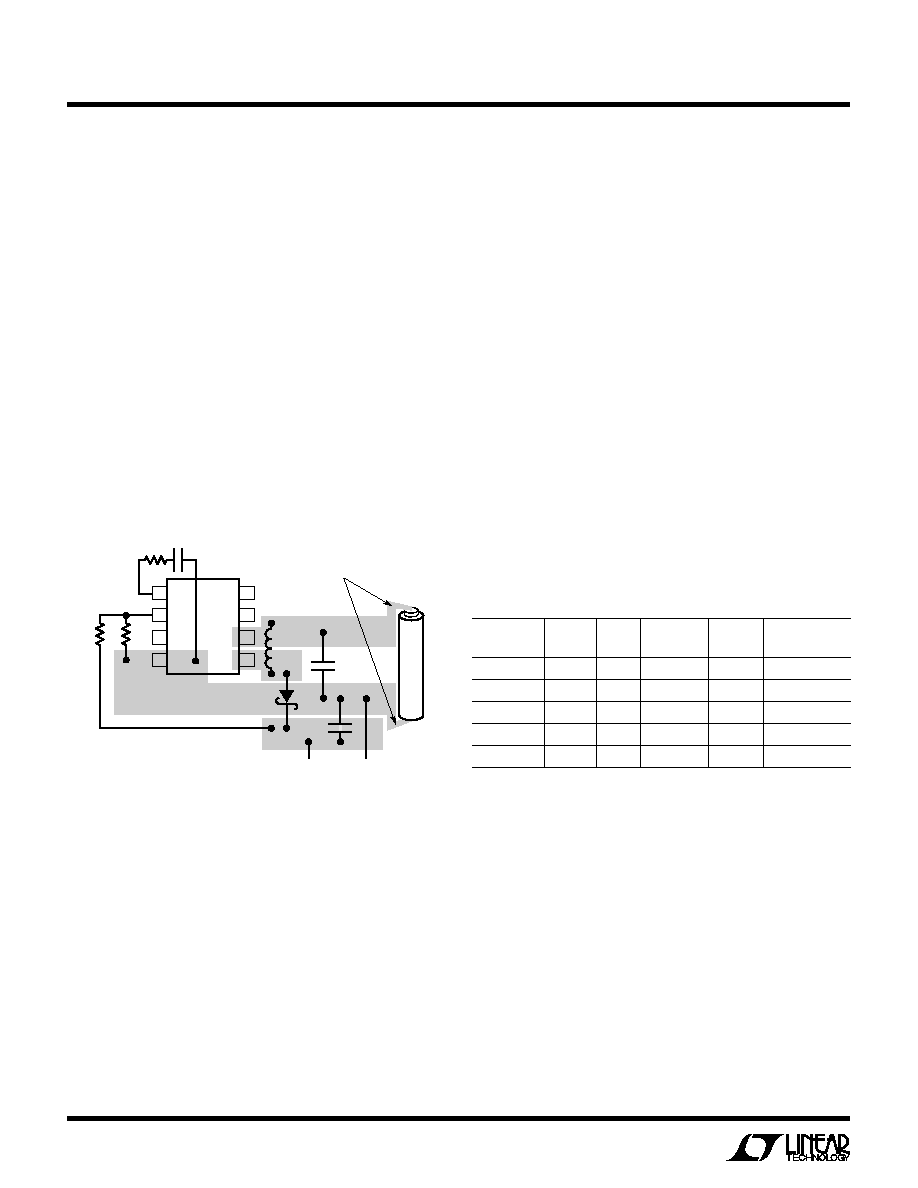
LAYOUT HINTS
The LT1307 switches current at high speed, mandating
careful attention to layout for proper performance.
You will
not get advertised performance with careless layouts.
Figure 12 shows recommended component placement.
Follow this closely in your PC layout. Note the direct path
of the switching loops. Input capacitor C
IN
must be placed
close (< 5mm) to the IC package. As little as 10mm of wire
or PC trace from C
IN
to V
IN
will cause problems such as
inability to regulate or oscillation. A 1
µ
F ceramic bypass
capacitor is the only input capacitance required
provided
the battery has a low inductance path to the circuit. The
battery itself provides the bulk capacitance the device
requires for proper operation. If the battery is located some
distance from the circuit, an additional input capacitor may
be required. A 100
µ
F aluminum electrolytic unit works well
in these cases. This capacitor need not have low ESR.
COMPONENT SELECTION
Inductors
Inductors appropriate for use with the LT1307 must pos-
sess three attributes. First, they must have low core loss at
600kHz. Most ferrite core units have acceptable losses at
this switching frequency. Inexpensive iron powder cores
should be viewed suspiciously, as core losses can cause
significant efficiency penalties at 600kHz. Second, the
inductor must handle current of 500mA without saturat-
ing. This places a lower limit on the physical size of the unit.
Molded chokes or chip inductors usually do not have
enough core to support 500mA current and are unsuitable
for the application. Lastly, the inductor should have low
DCR (copper wire resistance) to prevent efficiency-killing
I
2
R losses. Linear Technology has identified several induc-
tors suitable for use with the LT1307. This is not an
exclusive list. There are many magnetics vendors whose
components are suitable for use. A few vendor's compo-
nents are listed in Table 1.
Table 1. Inductors Suitable for Use with the LT1307
MAX
HEIGHT
PART
VALUE
DCR
MFR
(mm)
COMMENT
LQH3C100
10
µ
H
0.57
Murata-Erie
2.0
Smallest Size
DO1608-103
10
µ
H
0.16
Coilcraft
3.0
CD43-100
10
µ
H
0.18
Sumida
3.2
CD54-100
10
µ
H
0.10
Sumida
4.5
Best Efficiency
CTX32CT-100
10
µ
H
0.50
Coiltronics
2.2
1210 Footprint
Capacitors
For single cell applications, a 10
µ
F ceramic output capaci-
tor is generally all that is required. Ripple voltage in Burst
Mode can be reduced by increasing output capacitance.
For 2- and 3-cell applications, more than 10
µ
F is needed.
For a typical 2-cell to 5V application, a 47
µ
F to 100
µ
F low
ESR tantalum capacitor works well. AVX TPS series (100%
surge tested) or Sprague (don't be vague--ask for Sprague)
594D series are both good choices for low ESR capacitors.
Alternatively, a 10
µ
F ceramic in parallel with a low cost
(read high ESR) electrolytic capacitor, either tantalum or
aluminum, can be used instead. For through hole applica-
R2
KEEP TRACES
OR LEADS SHORT!
R1
C
IN
C
OUT
R
C
C
C
D
V
OUT
GROUND
1306 F12
1
2
3
4
8
LT1307
7
5
AA CELL
L
6
Figure 12. Recommended Component Placement. Traces
Carrying High Current Are Direct. Trace Area at FB Pin and V
C
Pin is Kept Low. Lead Length to Battery Should Be Kept Short
OPERATION FROM A LABORATORY POWER SUPPLY
If a lab supply is used, the leads used to connect the circuit
to the supply can have significant inductance at the
LT1307's switching frequency. As in the previous situa-
tion, an electrolytic capacitor may be required at the circuit
in order to reduce the AC impedance of the input suffi-
ciently. An alternative solution would be to attach the
circuit directly to the power supply at the supply terminals,
without the use of leads. The power supply's output
capacitance will then provide the bulk capacitance the
LT1307 circuit requires.
13
LT1307/LT1307B
APPLICATIO
N
S I
N
FOR
M
ATIO
N
W
U
U
U
tions where small size is not critical, Panasonic HFQ series
aluminum electrolytic capacitors have been found to per-
form well.
Table 2. Vendor Telephone Numbers
VENDOR
COMPONENTS
TELEPHONE
Coilcraft
Inductors
(708) 639-6400
Marcon
Capacitors
(708) 913-9980
Murata-Erie
Inductors, Capacitors
(404) 436-1300
Sumida
Inductors
(847) 956-0666
Tokin
Capacitors
(408) 432-8020
AVX
Capacitors
(207) 282-5111
Sprague
Capacitors
(603) 224-1961
Coiltronics
Inductors
(407) 241-7876
Diodes
Most of the application circuits on this data sheet specify
the Motorola MBR0520L surface mount Schottky diode.
This 0.5A, low drop diode complements the LT1307 quite
well. In lower current applications, a 1N4148 can be used,
although efficiency will suffer due to the higher forward
drop. This effect is particularly noticeable at low output
voltages. For higher voltage output applications, such as
LCD bias generators, the extra drop is a small percentage
of the output voltage so the efficiency penalty is small. The
low cost of the 1N4148 makes it attractive wherever it can
be used. In through hole applications the 1N5818 is the all
around best choice.
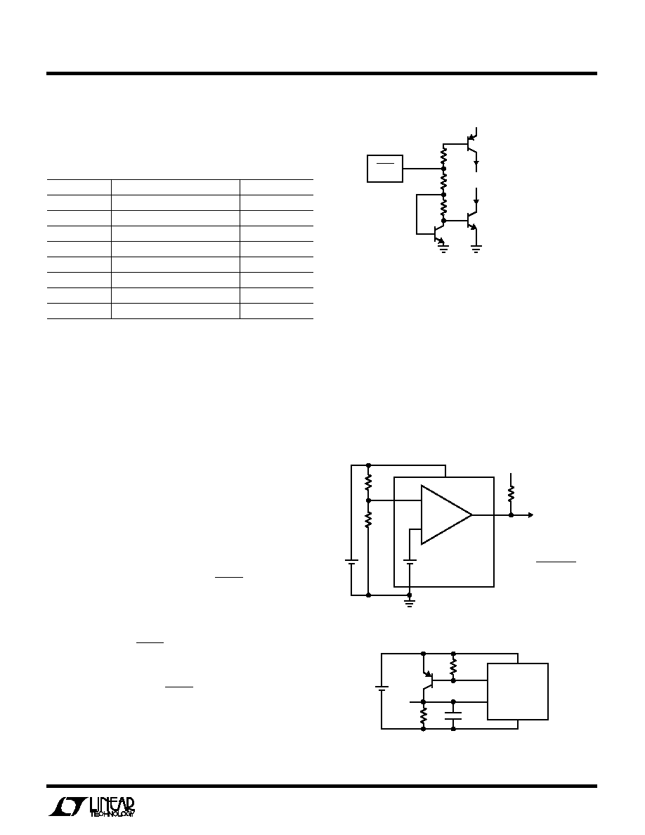
SHUTDOWN PIN
The LT1307 has a Shutdown pin (SHDN) that must be
grounded to shut the device down or tied to a voltage equal
or greater than V
IN
to operate. The shutdown circuit is
shown in Figure 13.
Note that allowing SHDN to float turns on both the start-
up current (Q2) and the shutdown current (Q3) for V
IN
>
2V
BE
. The LT1307 doesn't know what to do in this situation
and behaves erratically. SHDN voltage above V
IN
is al-
lowed. This merely reverse-biases Q3's base emitter junc-
tion, a benign condition.
Figure 13. Shutdown Circuit
V
IN
Q3
SHUTDOWN
CURRENT
R2
400k
200k
Q2
1307 F13
Q1
START-UP
CURRENT
SHDN
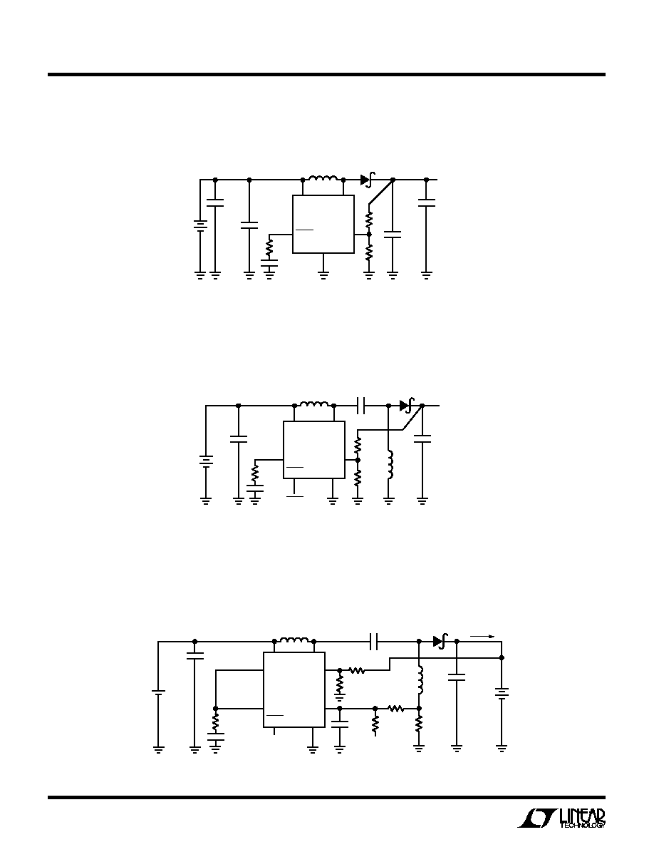
LOW-BATTERY DETECTOR
The LT1307's low-battery detector is a simple PNP input
gain stage with an open collector NPN output. The nega-
tive input of the gain stage is tied internally to a 200mV
±
5% reference. The positive input is the LBI pin. Arrange-
ment as a low-battery detector is straightforward. Figure
14 details hookup. R1 and R2 need only be low enough in
value so that the bias current of the LBI pin doesn't cause
large errors. For R2, 100k is adequate. The 200mV refer-
ence can also be accessed as shown in Figure 15.
LBO
LBI
TO PROCESSOR
R1
1M
R2
100k
V
IN
LT1307
1307 F14
3.3V
GND
200mV
INTERNAL
REFERENCE
≠
+
R1 =
V
LB
≠ 200mV
2
µ
A
Figure 14. Setting Low-Battery Detector Trip Point
V
IN
LT1307
LBI
LBO
200k
10
µ
F
GND
+
10k
1307 F15
2N3906
V
REF
200mV
Figure 15. Accessing 200mV Reference
14
LT1307/LT1307B
APPLICATIO
N
S I
N
FOR
M
ATIO
N
W
U
U
U
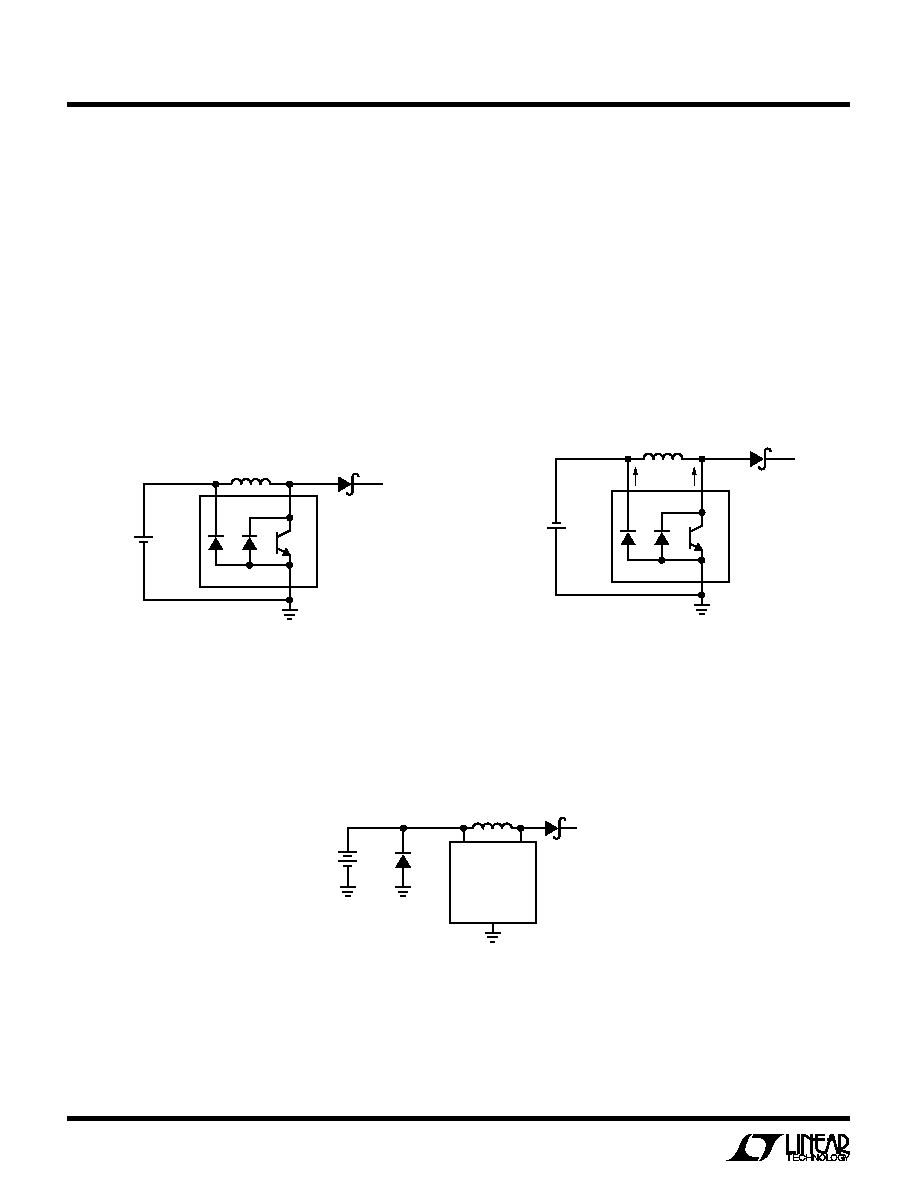
REVERSE BATTERY CONSIDERATIONS
The LT1307 is built on a junction-isolated bipolar process.
The p-type substrate is connected to the GND pin of the
LT1307. Substrate diodes, normally reverse-biased, are
present on the SW pin and the V
IN
pin as shown in Figure
16. When the battery polarity is reversed, these diodes
conduct, as illustrated in Figure 17. With a single AA or
AAA cell, several hundred milliamperes flow in the circuit.
The LT1307 can withstand this current without damage. In
laboratory tests, the LT1307 performed without degrada-
tion after sustaining polarity reversal for the life of a single
AA alkaline cell.
When using a 2- or 3-cell supply, an external protection
diode is recommended as shown in Figure 18. When the
battery polarity is reversed, the 1N4001 conducts, limiting
reverse voltage across the LT1307 to a single diode drop.
This arrangement will quickly deplete the cells' energy, but
it does prevent the LT1307 from excessive power dissipa-
tion and potential damage.
Figure 18. 1N4001 Diode Protects LT1307 from Excessive Power
Dissipation When a 2- or 3-Cell Battery is Used
V
IN
SW
LT1307
1N4001
1307 F18
2 OR 3
CELLS
GND
V
IN
LT1307
1307 F16
GND
1 CELL
1.5V
D2
SW
D1
Q1
Figure 16. LT1307 Showing Internal Substrate Diodes D1 and D2.
In Normal Operation Diodes are Reverse-Biased
V
IN
LT1307
CURRENT
FLOW
1307 F17
GND
1 CELL
≠ 1.5V
D2
SW
D1
Q1
Figure 17. When Cell Is Reversed Current Flows through
D1 and D2
15
LT1307/LT1307B
TYPICAL APPLICATIO
N
S
N
U
Externally Controlled Burst Mode Operation
This circuit overcomes the limitation of load-based
transitioning between Burst Mode operation and constant
switching mode by adding external control. If M1's gate is
grounded by an external open-drain signal, the converter
functions normally in constant switching mode, delivering
3.3V. Output noise is low, however efficiency at loads less
than 1mA is poor due to the 1mA supply current of the
LT1307B. If M1's gate is allowed to float, the low-battery
detector now drives the V
C
pin. R3 and R2 set the output
to 3V by allowing M1's gate to go to V
OUT
until the output
voltage drops below 3V. R1 adds hysteresis, resulting in
low-frequency Burst Mode operation ripple voltage at the
output. By pulling the V
C
pin below a V
BE
, quiescent
current of the LT1307B drops to 60
µ
A, resulting in accept-
able efficiency at loads in the 100
µ
A range.
V
IN
V
C
SW
FB
LBO
LBI
LT1307B
L1
10
µ
H
MBR0520
100k
2
CELLS
1nF
1
µ
F
CERAMIC
1307 F19
GND
SHDN
C2*
10
µ
F
CERAMIC
R3
698k
R4
1M
R2
499k
R5
590k
R1
10M
+
C1
100
µ
F
V
OUT
3.3V
200mA
300k
V
OUT
M1
2N7002
GROUND = HIGH POWER/LOW NOISE
FLOAT = Burst Mode OPERATION
SHUTDOWN
3.0V IN LOW-POWER
Burst Mode OPERATION
C1 =AVX TPSC107K006R0150
L1 = COILCRAFT DO1608-103
SUMIDA CD43-100
C2 OPTIONAL: REDUCES OUTPUT
RIPPLE CAUSED BY C1'S ESR
*
0.2s/DIV
1307 F20
This photo details output voltage as the circuit is switched
between the two modes. Load current is 100
µ
A in Burst
Mode operation; 10mA in constant switching mode.
This photo shows transient response in constant switch-
ing mode with a 10mA to 100mA stepped load. Output
ripple at the switching frequency can be reduced consid-
erably by adding a 10
µ
F ceramic capacitor in parallel with
the 100
µ
F tantalum.
10mA
100
µ
A
I
L
V
OUT
500mV/DIV
2ms/DIV
1307 F21
V
OUT
100mV/DIV
100mA
10mA
I
L
16
LT1307/LT1307B
TYPICAL APPLICATIO
N
S
N
U
Constant Current NiCd Battery Charger with Overvoltage Protection
for Acknowledge-Back Pagers
Step-Up/Step-Down Converter
Low Cost 2-Cell to 5V
V
IN
V
C
SW
FB
LT1307
L1
10
µ
H
L1*
∑
∑
MBR0520
V
IN
2.1V TO 4.8V
100k
3
CELLS
608k
1.02M
3.3V
100mA
1000pF
L1: COILTRONICS CTX10-1 OR 2 MURATA ERIE LQH3C100
EFFICIENCY
70% TO 73%
1307 TA03
1
µ
F
CERAMIC
2.2
µ
F
CERAMIC
GND
SHDN
SHDN
10
µ
F
CERAMIC
V
IN
V
C
SW
FB
LBO
LBI
LT1307
L1
10
µ
H
V
IN
1.8V TO 1V
∑
MBR0520L
47k
1 CELL
AA OR
AAA
2200pF
1
µ
F
2
3
L1: COILTRONICS CTX10-1
1307 TA04
1nF
3V
200mV
15mA
≠100mV
3 CELLS
NiCd
2.2
µ
F
CERAMIC
GND
SHDN
1 = CHARGE
0 = SHUTDOWN
323k
280k
6.7
1M
OVERVOLTAGE
PROTECTION
1
µ
F
CERAMIC
1
4
30k
∑
V
IN
SW
FB
LT1307
V
IN
1.4V TO 3.3V
L1
10
µ
H
1N5818
SHDN
100k
323k
1M
5V
100mA
4700pF
C1, C2: PANASONIC ECA0JFQ221
(DIGI-KEY P5604-ND)
L1: SUMIDA CD43-100
1307 TA02
C1*
220
µ
F
6.3V
0.1
µ
F
GND
+
0.1
µ
F
C2
220
µ
F
6.3V
+
17
LT1307/LT1307B
TYPICAL APPLICATIO
N
S
N
U
Single Cell Powered Constant Current LED Driver
C1
1
µ
F
CERAMIC
L1
10
µ
H
D1
V
IN
1307 TA05
NC
D2
40mA
R1
5.1
100k
ON/OFF
V
IN
R2
22k
100k
C2
1
µ
F
CERAMIC
Q1
2N3906
AA
CELL
C3
22
µ
F
+
L1:MURATA-ERIE LQH3C100K04
D1:1N4148
C1, C2:CERAMIC
D2, D3:LUMEX SSL-X100133SRC/4 "MEGA-BRITE" RED LED
OR PANASONIC LNG992CF9 HIGH BRIGHTNESS BLUE LED
V
IN
SW
FB
LT1307B
LBI
LBO
SHDN
V
C
GND
Flash Memory VPP Supply
V
IN
SW
FB
LT1307
L1
10
µ
H
D1
47k
232k
1%
2M
1%
1307 TA09
0.33
µ
F
CERAMIC
◊
2
12V/30mA FROM 3V
12V/60mA FROM 5V
~250mV
P-P
RIPPLE
0.33
µ
F
V
C
GND
SHDN
SHUTDOWN
D1: MOTOROLA MBR0520L
L1: MURATA-ERIE LQH3C100K04
1
µ
F
TANTALUM
2000pF
1N4148
V
IN
3V TO 5.5V
+
10pF
High Voltage Flyback Converter
V
IN
V
IN
1V TO 5V
SW
1N4148
4
6
3
1
∑
∑
LT1307
FB
SHDN
SHUTDOWN
V
C
100k
1000pF
GND
R2
240k
1%
R1
2V
OUT
V
OUT
0.1
µ
F
1
µ
F
CERAMIC
0.01
µ
F
0.1
µ
F
1307 TA06
OPTIONAL
DOUBLER
T1
1:12
T1: DALE LPE3325-A190, n = 12 (605) 665-9301
MAXIMUM DUTY CYCLE:
80%
FOR FLYBACK, V
OUT
=
n(V
IN
≠ V
SW
)
V
OUT
= 1.22V 1 +
( )
R1
R2
DC
1 ≠ DC
FOR 1V
IN
, MAXIMUM V
OUT
=
FOR 2V
IN
, MAXIMUM V
OUT
85V.
HIGHER VOLTAGES ACHIEVED WITH CAPACITIVE DOUBLER OR TRIPLER
NO SNUBBER REQUIRED WITH SPECIFIED TRANSFORMER AND V
IN
< 5V
12(1 ≠ 0.2)
37V
0.8
1 ≠ 0.8
18
LT1307/LT1307B
TYPICAL APPLICATIO
N
S
N
U
Single Cell CCFL Power Supply
V
IN
V
C
D1
100
4
3
CCFL
2
1.5V
5
T1
1
1307 TA08
6
10
SW
FB
0.1
µ
F
C1
0.1
µ
F
1
CELL
1.5V
1.5V
1k
L1
33
µ
H
LT1307B
1 = OPERATE
0 = SHUTDOWN
C1: WIMA MKP-20
D1: MOTOROLA MBR0520L
L1: SUMIDA CD54-330
T1: COILTRONICS CTX110611
Q1, Q2: ZETEX FZT-849
GND
SHDN
10k
DIMMING
0.1
µ
F
1N4148
1N4148
1
µ
F
CERAMIC
10k
47pF
3kV
Q1
Q2
Dimensions in inches (millimeters) unless otherwise noted.
PACKAGE DESCRIPTIO
N
U
MS8 Package
8-Lead Plastic MSOP
(LTC DWG # 05-08-1660)
MSOP08 0596
* DIMENSION DOES NOT INCLUDE MOLD FLASH, PROTRUSIONS OR GATE BURRS. MOLD FLASH,
PROTRUSIONS OR GATE BURRS SHALL NOT EXCEED 0.006" (0.152mm) PER SIDE
** DIMENSION DOES NOT INCLUDE INTERLEAD FLASH OR PROTRUSIONS.
INTERLEAD FLASH OR PROTRUSIONS SHALL NOT EXCEED 0.006" (0.152mm) PER SIDE
1
2
3
4
0.192
±
0.004
(4.88
±
0.10)
8
7 6
5
0.118
±
0.004*
(3.00
±
0.10)
0.118
±
0.004**
(3.00
±
0.10)
0.021
±
0.004
(0.53
±
0.01)
0
∞
≠ 6
∞
TYP
SEATING
PLANE
0.007
(0.18)
0.040
±
0.006
(1.02
±
0.15)
0.012
(0.30)
0.006
±
0.004
(0.15
±
0.10)
0.025
(0.65)
TYP
19
LT1307/LT1307B
Dimensions in inches (millimeters) unless otherwise noted.
PACKAGE DESCRIPTIO
N
U
S8 Package
8-Lead Plastic Small Outline (Narrow 0.150)
(LTC DWG # 05-08-1610)
1
2
3
4
0.150 ≠ 0.157**
(3.810 ≠ 3.988)
8
7
6
5
0.189 ≠ 0.197*
(4.801 ≠ 5.004)
0.228 ≠ 0.244
(5.791 ≠ 6.197)
0.016 ≠ 0.050
0.406 ≠ 1.270
0.010 ≠ 0.020
(0.254 ≠ 0.508)
◊
45
∞
0
∞
≠ 8
∞
TYP
0.008 ≠ 0.010
(0.203 ≠ 0.254)
SO8 0695
0.053 ≠ 0.069
(1.346 ≠ 1.752)
0.014 ≠ 0.019
(0.355 ≠ 0.483)
0.004 ≠ 0.010
(0.101 ≠ 0.254)
0.050
(1.270)
BSC
DIMENSION DOES NOT INCLUDE MOLD FLASH. MOLD FLASH
SHALL NOT EXCEED 0.006" (0.152mm) PER SIDE
DIMENSION DOES NOT INCLUDE INTERLEAD FLASH. INTERLEAD
FLASH SHALL NOT EXCEED 0.010" (0.254mm) PER SIDE
*
**
N8 Package
8-Lead PDIP (Narrow 0.300)
(LTC DWG # 05-08-1510)
N8 0695
0.005
(0.127)
MIN
0.100
±
0.010
(2.540
±
0.254)
0.065
(1.651)
TYP
0.045 ≠ 0.065
(1.143 ≠ 1.651)
0.130
±
0.005
(3.302
±
0.127)
0.015
(0.380)
MIN
0.018
±
0.003
(0.457
±
0.076)
0.125
(3.175)
MIN
1
2
3
4
8
7
6
5
0.255
±
0.015*
(6.477
±
0.381)
0.400*
(10.160)
MAX
0.009 ≠ 0.015
(0.229 ≠ 0.381)
0.300 ≠ 0.325
(7.620 ≠ 8.255)
0.325
+0.025
≠0.015
+0.635
≠0.381
8.255
(
)
*THESE DIMENSIONS DO NOT INCLUDE MOLD FLASH OR PROTRUSIONS.
MOLD FLASH OR PROTRUSIONS SHALL NOT EXCEED 0.010 INCH (0.254mm)
Information furnished by Linear Technology Corporation is believed to be accurate and reliable.
However, no responsibility is assumed for its use. Linear Technology Corporation makes no represen-
tation that the interconnection of its circuits as described herein will not infringe on existing patent rights.
20
LT1307/LT1307B
©
LINEAR TECHNOLOGY CORPORATION 1995
Linear Technology Corporation
1630 McCarthy Blvd., Milpitas, CA 95035-7417
(408) 432-1900
q
FAX
: (408) 434-0507
q
TELEX
: 499-3977
TYPICAL APPLICATIO
N
U
LCD Bias Generator
LT/GP 1196 7K ∑ PRINTED IN THE USA
PART NUMBER
DESCRIPTION
COMMENTS
LTC
Æ
1163
Triple High Side Driver for 2-Cell Inputs
1.8V Minimum Input, Drives N-Channel MOSFETs
LTC1174
Micropower Step-Down DC/DC Converter
94% Efficiency, 130
µ
A I
Q
, 9V to 5V at 300mA
LT1302
High Output Current Micropower DC/DC Converter
5V/600mA from 2V, 2A Internal Switch, 200
µ
A I
Q
LT1304
2-Cell Micropower DC/DC Converter
Low-Battery Detector Active in Shutdown
LTC1440/1/2
Ultralow Power Single/Dual Comparators with Reference
2.8
µ
A I
Q
, Adjustable Hysteresis
LTC1516
2-Cell to 5V Regulated Charge Pump
12
µ
A I
Q
, No Inductors, 5V at 50mA from 3V Input
LT1521
Micropower Low Dropout Linear Regulator
500mV Dropout, 300mA Current, 12
µ
A I
Q
RELATED PARTS
V
IN
V
C
SW
FB
LT1307
L1
D3
D2
D1
100k
1, 2 OR 3
CELLS
1M
100k
PWM IN 3.3V, 0% TO 100%
215k
3.3M
V
OUT
16V TO 24V
5mA FROM 1 CELL
15mA FROM 2 CELLS
35mA FROM 3 CELLS
≠V
OUT
4700pF
10pF
L1: 3.3
µ
H (1 CELL)
4.7
µ
H (2 CELLS)
10
µ
H (3 CELLS)
SUMIDA CD43
MURATA-ERIE LQH3C
COILCRAFT D01608
C1:1
µ
F FOR +OUTPUT
0.01
µ
F FOR ≠ OUTPUT
D1 TO D3: MBR0530 OR 1N4148
1307 TA07
1
µ
F
3.3
µ
F
0.1
µ
F
GND
SHDN
SHUTDOWN
C1
1
µ
F
+