1
LT1308A/LT1308B
FEATURES
DESCRIPTIO
N
U
APPLICATIO
N
S
U
TYPICAL APPLICATIO
N
U
, LTC and LT are registered trademarks of Linear Technology Corporation.
Final Electrical Specifications
High Current, Micropower
Single Cell, 600kHz
DC/DC Converters
August 1999
s
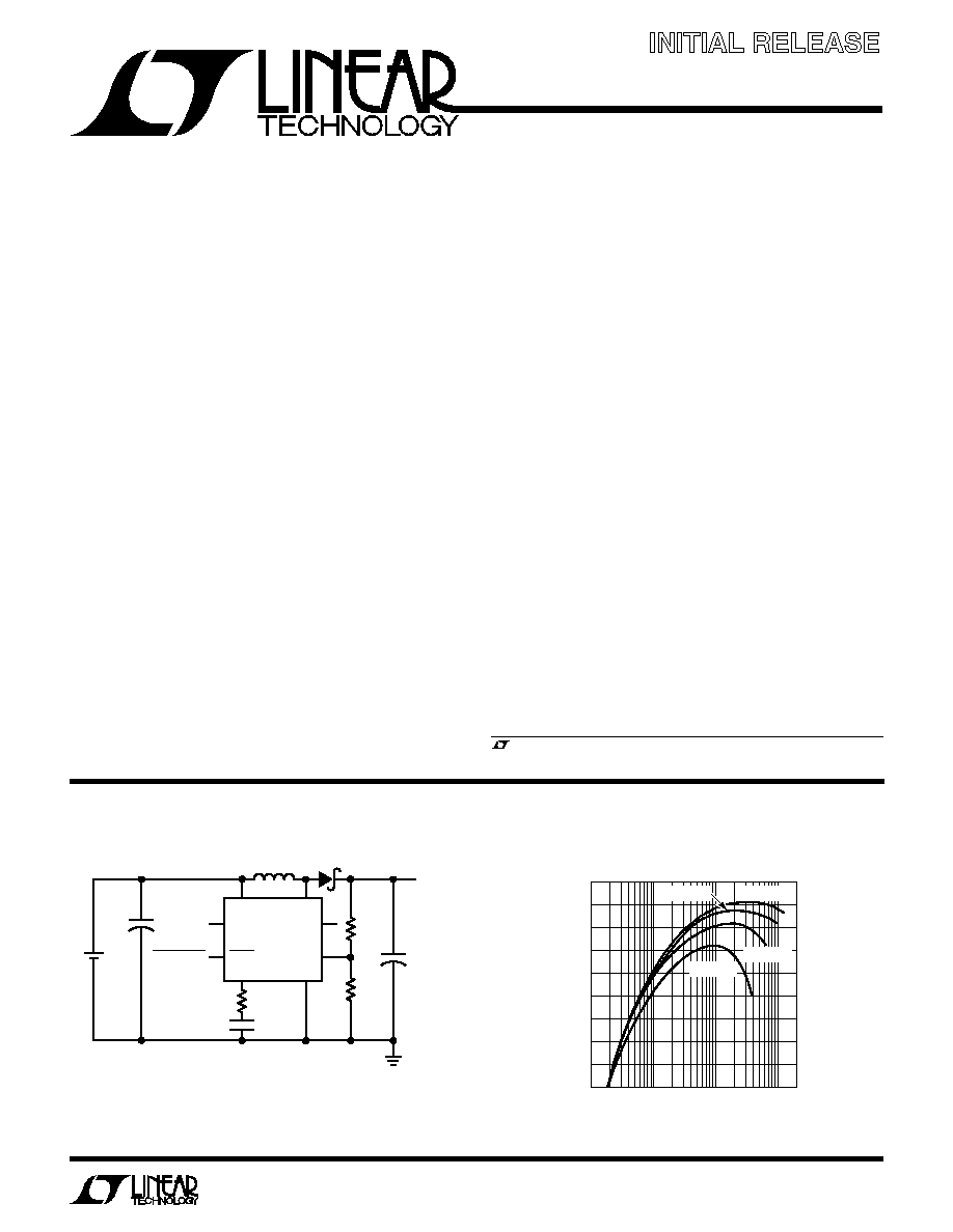
5V at 1A from a Single Li-Ion Cell
s
5V at 800mA in SEPIC Mode from Four NiCd Cells
s
Fixed Frequency Operation: 600kHz
s
Boost Converter Outputs up to 34V
s
Starts into Heavy Loads
s
Automatic Burst Mode
TM
Operation at
Light Load (LT1308A)
s
Continuous Switching at Light Loads (LT1308B)
s
Low V
CESAT
Switch: 300mV at 2A
s
Pin-for-Pin Upgrade Compatible with LT1308
s
Lower Quiescent Current in Shutdown: 1
�
A (Max)
s
Improved Accuracy Low-Battery Detector
Reference: 200mV
�
2%
s
GSM/CDMA Phones
s
Digital Cameras
s
LCD Bias Supplies
s
Answer-Back Pagers
s
GPS Receivers
s
Battery Backup Supplies
s
Handheld Computers
The LT
�
1308A/LT1308B are micropower, fixed frequency
step-up DC/DC converters that operate over a 1V to 10V
input voltage range. They are improved versions of the
LT1308 and are recommended for use in new designs. The
LT1308A features automatic shifting to power saving
Burst Mode operation at light loads and consumes just
140
�
A at no load. The LT1308B features continuous
switching at light loads and operates at a quiescent current
of 2.5mA. Both devices consume less than 1
�
A in
shutdown.
Low-battery detector accuracy is significantly tighter than
the LT1308. The 200mV reference is specified at
�
2% at
room and
�
3% over temperature. The shutdown pin
enables the device when it is tied to a 1V or higher source
and does not need to be tied to V
IN
as on the LT1308. An
internal V
C
clamp results in improved transient response
and the switch voltage rating has been increased to 36V,
enabling higher output voltage applications.
The LT1308A/LT1308B are available in the 8-lead SO and
14-lead TSSOP packages.
Burst Mode is a trademark of Linear Technology Corporation.
Information furnished by Linear Technology Corporation is believed to be accurate and reliable.
However, no responsibility is assumed for its use. Linear Technology Corporation makes no represen-
tation that the interconnection of its circuits as described herein will not infringe on existing patent rights.
Figure 1. LT1308B Single Li-Ion Cell to 5V/1A DC/DC Converter
V
IN
SW
FB
LT1308B
L1
4.7
�
H
D1
LBO
LBI
47k
R2
100k
R1*
309k
5V
1A
100pF
1308A/B F01
C1
47
�
F
C2
220
�
F
Li-Ion
CELL
V
C
GND
SHDN
SHUTDOWN
C1: AVX TAJC476M010
C2: AVX TPSD227M006
D1: IR 10BQ015
+
+
L1: MURATA LQH6N4R7
*R1: 169k FOR V
OUT
= 3.3V
887k FOR V
OUT
= 12V
Converter Efficiency
LOAD CURRENT (mA)
1
EFFICIENCY (%)
95
90
85
80
75
70
65
60
55
50
10
100
1000
1308A/B F01a
V
IN
= 4.2V
V
IN
= 1.5V
V
IN
= 2.5V
V
IN
= 3.6V

2
LT1308A/LT1308B
A
U
G
W
A
W
U
W
A
R
BSOLUTE
XI
TI
S
ORDER PART
NUMBER
W
U
U
PACKAGE/ORDER I FOR ATIO
ELECTRICAL C
C
HARA TERISTICS
(Note 1)
V
IN
, SHDN, LBO Voltage ......................................... 10V
SW Voltage ............................................... � 0.4V to 36V
FB Voltage ....................................................... V
IN
+ 1V
V
C
Voltage ................................................................ 2V
LBI Voltage ................................................. � 0.1V to 1V
Current into FB Pin ..............................................
�
1mA
S8 PART MARKING
LT1308ACS8
LT1308AIS8
LT1308BCS8
LT1308BIS8
The
q
denotes specifications which apply over the full operating temperature range, otherwise specifications are T
A
= 25
�
C.
Commercial Grade 0
�
C to 70
�
C. V
IN
= 1.1V, V
SHDN
= V
IN
, unless otherwise noted.
SYMBOL
PARAMETER
CONDITIONS
MIN
TYP
MAX
UNITS
I
Q
Quiescent Current
Not Switching, LT1308A
140
240
�
A
Switching, LT1308B
2.5
4
mA
V
SHDN
= 0V (LT1308A/LT1308B)
0.01
1
�
A
V
FB
Feedback Voltage
q
1.20
1.22
1.24
V
I
B
FB Pin Bias Current
(Note 3)
q
27
80
nA
Reference Line Regulation
1.1V
V
IN
2V
q
0.03
0.4
%/V
2V
V
IN
10V
0.01
0.2
%/V
Minimum Input Voltage
0.92
1
V
g
m
Error Amp Transconductance
I = 5
�
A
60
�
mhos
A
V
Error Amp Voltage Gain
100
V/V
f
OSC
Switching Frequency
V
IN
= 1.2V
q
500
600
700
kHz
Maximum Duty Cycle
q
82
90
%
Switch Current Limit
Duty Cyle = 30% (Note 4)
2
3
4.5
A
Switch V
CESAT
I
SW
= 2A (25
�
C, 0
�
C), V
IN
= 1.5V
290
350
mV
I
SW
= 2A (70
�
C), V
IN
= 1.5V
330
400
mV
Burst Mode Operation Switch Current Limit
V
IN
= 2.5V, Circuit of Figure 1
400
mA
(LT1308A)
T
JMAX
= 125
�
C,
JA
= 80
�
C/W
1308B
1308BI
1308A
1308AI
Consult factory for Military grade parts.
1
2
3
4
8
7
6
5
TOP VIEW
LBO
LBI
V
IN
SW
V
C
FB
SHDN
GND
S8 PACKAGE
8-LEAD PLASTIC SO
Operating Temperature Range
Commercial ............................................ 0
�
C to 70
�
C
Extended Commerial (Note 2) ........... � 40
�
C to 85
�
C
Industrial ........................................... � 40
�
C to 85
�
C
Storage Temperature Range ................ � 65
�
C to 150
�
C
Lead Temperature (Soldering, 10 sec)................. 300
�
C
ORDER PART
NUMBER
LT1308ACF
LT1308BCF
T
JMAX
= 125
�
C,
JA
= 80
�
C/W
F PACKAGE
14-LEAD PLASTIC TSSOP
1
2
3
4
5
6
7
TOP VIEW
14
13
12
11
10
9
8
V
C
FB
SHDN
GND
GND
GND
GND
LBO
LBI
V
IN
V
IN
SW
SW
SW
(Note 6)
3
LT1308A/LT1308B
ELECTRICAL C
C
HARA TERISTICS
The
q
denotes specifications which apply over the full operating temperature range, otherwise specifications are T
A
= 25
�
C.
Industrial Grade � 40
�
C to 85
�
C. V
IN
= 1.2V, V
SHDN
= V
IN
, unless otherwise noted.
SYMBOL
PARAMETER
CONDITIONS
MIN
TYP
MAX
UNITS
I
Q
Quiescent Current
Not Switching, LT1308A
q
140
240
�
A
Switching, LT1308B
q
2.5
4
mA
V
SHDN
= 0V (LT1308A/LT1308B)
q
0.01
1
�
A
V
FB
Feedback Voltage
q
1.19
1.22
1.25
V
I
B
FB Pin Bias Current
(Note 3)
q
27
80
nA
Reference Line Regulation
1.1V
V
IN
2V
q
0.05
0.4
%/V
2V
V
IN
10V
q
0.01
0.2
%/V
Minimum Input Voltage
0.92
1
V
g
m
Error Amp Transconductance
I = 5
�
A
60
�
mhos
A
V
Error Amp Voltage Gain
100
V/V
f
OSC
Switching Frequency
q
500
600
750
kHz
Maximum Duty Cycle
q
82
90
%
Switch Current Limit
Duty Cyle = 30% (Note 4)
2
3
4.5
A
Switch V
CESAT
I
SW
= 2A (25
�
C, � 40
�
C), V
IN
= 1.5V
290
350
mV
I
SW
= 2A (85
�
C), V
IN
= 1.5V
330
400
mV
Burst Mode Operation Switch Current Limit
V
IN
= 2.5V, Circuit of Figure 1
400
mA
(LT1308A)
Shutdown Pin Current
V
SHDN
= 1.1V
q
2
5
�
A
V
SHDN
= 6V
q
20
35
�
A
V
SHDN
= 0V
0.01
0.1
�
A
LBI Threshold Voltage
196
200
204
mV
q
193
200
207
mV
LBO Output Low
I
SINK
= 50
�
A
q
0.1
0.25
V
LBO Leakage Current
V
LBI
= 250mV, V
LBO
= 5V
q
0.01
0.1
�
A
LBI Input Bias Current (Note 5)
V
LBI
= 150mV
33
100
nA
Low-Battery Detector Gain
3000
V/V
Switch Leakage Current
V
SW
= 5V
q
0.01
10
�
A
The
q
denotes specifications which apply over the full operating temperature range, otherwise specifications are T
A
= 25
�
C.
Commercial Grade 0
�
C to 70
�
C. V
IN
= 1.1V, V
SHDN
= V
IN
, unless otherwise noted.
SYMBOL
PARAMETER
CONDITIONS
MIN
TYP
MAX
UNITS
Shutdown Pin Current
V
SHDN
= 1.1V
q
2
5
�
A
V
SHDN
= 6V
q
20
35
�
A
V
SHDN
= 0V
q
0.01
0.1
�
A
LBI Threshold Voltage
196
200
204
mV
q
194
200
206
mV
LBO Output Low
I
SINK
= 50
�
A
q
0.1
0.25
V
LBO Leakage Current
V
LBI
= 250mV, V
LBO
= 5V
q
0.01
0.1
�
A
LBI Input Bias Current (Note 5)
V
LBI
= 150mV
33
100
nA
Low-Battery Detector Gain
3000
V/V
Switch Leakage Current
V
SW
= 5V
q
0.01
10
�
A
4
LT1308A/LT1308B
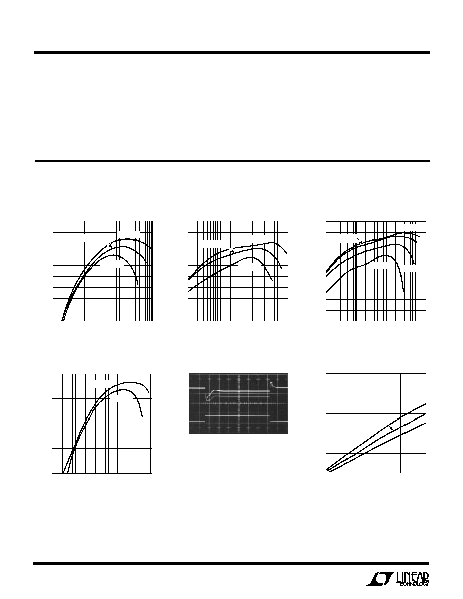
TYPICAL PERFOR
M
A
N
CE CHARACTERISTICS
U
W
LT1308B
3.3V Output Efficiency
LT1308A
5V Output Efficiency
LT1308A
3.3V Output Efficiency
LT1308B
12V Output Efficiency
Switch Saturation Voltage
vs Current
LT1308A Transient Response
Circuit of Figure 1
V
OUT
100mV/DIV
AC COUPLED
1A
0A
I
LOAD
V
IN
= 3.6V
100
�
s/DIV
V
OUT
= 5V
C
OUT
= 220
�
F
1308 G05
Note 4: Switch current limit guaranteed by design and/or correlation to
static tests. Duty cycle affects current limit due to ramp generator (see
Block Diagram).
Note 5: Bias current flows out of LBI pin.
Note 6: Connect the four GND pins (Pins 4�7) together at the device.
Similarly, connect the three SW pins (Pins 8�10) together and the two V
IN
pins (Pins 11, 12) together at the device.
Note 1: Absolute Maximum Ratings are those values beyond which the life
of a device may be impaired.
Note 2: The LT1308ACS8 and LT1308BCS8 are designed, characterized
and expected to meet the industrial temperature limits, but are not tested
at �40
�
C and 85
�
C. I grade devices are guaranteed.
Note 3: Bias current flows into FB pin.
ELECTRICAL C
C
HARA TERISTICS
LOAD CURRENT (mA)
95
90
85
80
75
70
65
60
55
50
1
100
1000
1308A/B G01
10
EFFICIENCY (%)
V
IN
= 1.8V
V
IN
= 2.5V
V
IN
= 1.2V
LOAD CURRENT (mA)
95
90
85
80
75
70
65
60
55
50
1
100
1000
1308A/B G02
10
EFFICIENCY (%)
V
IN
= 1.8V
V
IN
= 2.5V
V
IN
= 1.2V
LOAD CURRENT (mA)
1
EFFICIENCY (%)
95
90
85
80
75
70
65
60
55
50
10
100
1000
1308A/B G03
V
IN
= 4.2V
V
IN
= 2.5V
V
IN
= 3.6V
V
IN
= 1.5V
LOAD CURRENT (mA)
90
85
80
75
70
65
60
55
50
1
100
1000
1308A/B G04
10
EFFICIENCY (%)
V
IN
= 5V
V
IN
= 3.3V
SWITCH CURRENT (A)
0
SWITCH V
CESAT
(mV)
2.0
85
�
C
1308 G06
0.5
1.0
1.5
500
400
300
200
100
0
25
�
C
�40
�
C
5
LT1308A/LT1308B
V
C
(Pin 1): Compensation Pin for Error Amplifier. Con-
nect a series RC from this pin to ground. Typical values
are 47k
and 100pF. Minimize trace area at V
C
.
FB (Pin 2): Feedback Pin. Reference voltage is 1.22V.
Connect resistive divider tap here. Minimize trace area at
FB. Set V
OUT
according to: V
OUT
= 1.22V(1 + R1/R2).
SHDN (Pin 3): Shutdown. Ground this pin to turn off
switcher. To enable, tie to 1V or more. SHDN does not
need to be at V
IN
to enable the device.
GND (Pin 4): Ground. Connect directly to local ground
plane. Ground plane should enclose all components
associated with the LT1308. PCB copper connected to
Pin 4 also functions as a heat sink. Maximize this area to
keep chip heating to a minimum.
PI
N
FU
N
CTIO
N
S
U
U
U
SW (Pin 5): Switch Pin. Connect inductor/diode here.
Minimize trace area at this pin to keep EMI down.
V
IN
(Pin 6): Supply Pin. Must have local bypass capacitor
right at the pin, connected directly to ground.
LBI (Pin 7): Low-Battery Detector Input. 200mV refer-
ence. Voltage on LBI must stay between �100mV and 1V.
Low-battery detector does not function with SHDN pin
grounded. If not used, float LBI pin.
LBO (Pin 8): Low-Battery Detector Output. Open collec-
tor, can sink 50
�
A. A 1M
pull-up is recommended. LBO
is high impedance when SHDN is grounded.
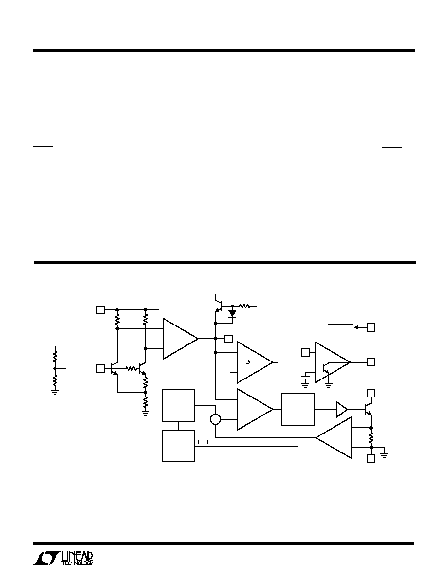
�
+
�
+
�
+
�
+
�
+
+
+
COMPARATOR
RAMP
GENERATOR
R
BIAS
V
C
2V
BE
g
m
Q2
�
10
Q1
FB
FB
ENABLE
*HYSTERESIS IN LT1308A ONLY
200mV
A = 3
FF
A2
A1
Q4
*
ERROR
AMPLIFIER
A4
0.03
DRIVER
SW
GND
1308 BD
Q3
Q
S
600kHz
OSCILLATOR
5
LBO
LBI
SHDN
SHUTDOWN
3
7
1
4
R6
40k
R5
40k
R1
(EXTERNAL)
R3
30k
R4
140k
2
V
IN
V
IN
V
IN
V
OUT
6
8
R2
(EXTERNAL)
BLOCK DIAGRA
M
W
Figure 2. LT1308A/LT1308B Block Diagram