 | ÐлекÑÑоннÑй компоненÑ: LT1309CS8 | СкаÑаÑÑ:  PDF PDF  ZIP ZIP |
Äîêóìåíòàöèÿ è îïèñàíèÿ www.docs.chipfind.ru
1
LT1309
The LT
®
1309 is a 500kHz micropower DC/DC converter
for Flash Memory. The regulator features Burst Mode
TM
operation with a 0.5A, 300mV switch, enabling 85%
efficiency at the fixed 12V output. High frequency opera-
tion permits the use of small value, and therefore small
size, surface mount inductors and capacitors. The LT1309
comes in an 8-lead SO package allowing extremely
compact PC board layouts. These features make the
device attractive for PCMCIA cards, cellular phones and
other applications where PC board space is limited.
Quiescent current is 650
µ
A decreasing to 9
µ
A when the
part shuts down. The device includes a soft start feature
which limits supply current transients during turn-on.
The LT1309 contains a VPP VALID comparator with a
logic output that goes low when the output voltage is
ready to program 12V Flash Memory. This comparator
simplifies the interface to external control logic.
500kHz Micropower
DC/DC Converter
for Flash Memory
S
FEATURE
D
U
ESCRIPTIO
s
60mA Output Current at 12V from 3V or 5V Supply
s
Shutdown to 9
µ
A
s
VPP VALID Comparator
s
Up to 85% Efficiency
s
Switching Frequency: 500kHz (Typical)
s
Quiescent Current: 650
µ
A
s
Low V
CESAT
Switch: 300mV at 0.5A (Typical)
s
Soft Start Reduces Supply Current Transients
s
Uses Low Value, Small Size,
Surface Mount Inductors
s
Available in 8-Lead SO Package
U
A
O
PPLICATI
TYPICAL
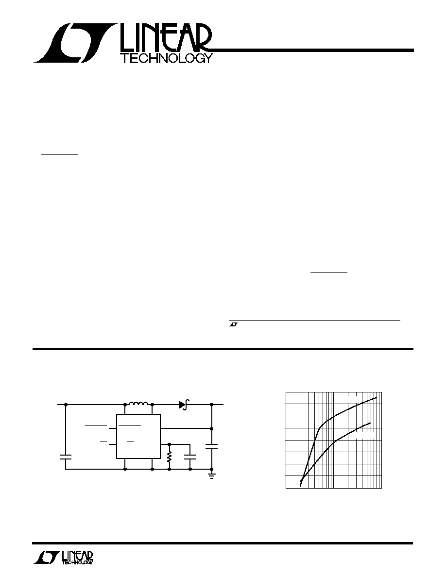
12V, 60mA Flash Memory Programming Supply
12V Output Efficiency
LOAD CURRENT (mA)
1
70
EFFICIENCY (%)
72
74
76
78
86
10
100
LT1309 · TA02
80
82
84
V
IN
= 5V
V
IN
= 3.3V
V
IN
V
SW
L1*
10
µ
H
D1
VPP 12V, 60mA
SENSE
VPP VALID
LT1309
ON/OFF
VPP VALID
R1
1M
LT1309 · TA01
C3
0.1
µ
F
C2
1
µ
F**
C1
4.7
µ
F
MURATA ERIE LQH3C100K0YM00
CERAMIC
MOTOROLA MBR0530
*
**
ON/OFF
V
IN
3.3V TO 5V
SOFT
START
PGND
GND
+
U
S
A
O
PPLICATI
s
Flash Memory VPP Generators
s
Type II and III PCMCIA Card DC/DC Converters
s
3V to 12V, 5V to 12V Converters
s
Portable Computers and Instruments
s
Cellular Telephones
s
DC/DC Converter Module Replacements
, LTC and LT are registered trademarks of Linear Technology Corporation.
Burst Mode is a trademark of Linear Technology Corporation.
2
LT1309
A
U
G
W
A
W
U
W
A
R
BSOLUTE
XI
TI
S
V
CC
Voltage ............................................................... 7V
V
SW
Voltage ............................................................ 20V
V
SENSE
Voltage ....................................................... 20V
V
ON/OFF
Voltage......................................................... 7V
V
SEL
Voltage ............................................................. 7V
I
LIM
Voltage .............................................................. 7V
Maximum Power Dissipation ............................ 500mW
Operating Temperature Range ..................... 0
°
C to 70
°
C
Storage Temperature Range ................. 65
°
C to 150
°
C
Lead Temperature (Soldering, 10 sec).................. 300
°
C
W
U
U
PACKAGE/ORDER I FOR ATIO
ORDER PART
NUMBER
S8 PART MARKING
ELECTRICAL C
C
HARA TERISTICS
T
A
= 25
°
C, V
CC
= 5V, V
ON/OFF
= 3V, unless otherwise noted.
SYMBOL
PARAMETER
CONDITIONS
MIN
TYP
MAX
UNITS
I
Q
Quiescent Current
V
SENSE
= 12V
650
900
µ
A
Quiescent Current, Shutdown
V
ON/OFF
= 0.2V
9
15
µ
A
Input Voltage Range
2
6
V
Output Sense Voltage
q
11.5
12
12.6
V
Output Referred Comparator Hysteresis
35
mV
f
OSC
Oscillator Frequency
Current Limit Not Asserted
400
500
700
kHz
DC
Maximum Duty Cycle
q
80
85
92
%
t
ON
Switch ON Time
1.7
µ
s
Reference Line Regulation
2V < V
IN
< 6V
0.06
0.15
%/V
V
CESAT
Switch Saturation Voltage
I
SW
= 0.5A
230
350
mV
Switch Leakage Current
V
SW
= 12V, Switch Off
0.1
10
µ
A
Switch Current Limit
V
IN
= 5V, Soft Start Floating
400
600
900
mA
V
IN
= 3V, Soft Start Floating
450
650
950
mA
Soft Start Current
Soft Start Grounded
80
120
µ
A
ON/OFF Input Voltage Low
0.8
V
ON/OFF Input Voltage High
1.6
V
ON/OFF Bias Current
V
ON/OFF
= 5V
16.0
24.0
µ
A
V
ON/OFF
= 3V
8.0
14.0
µ
A
V
ON/OFF
= 0V
0.1
1.0
µ
A
Sense Pin Input Current
50.0
90
µ
A
V
ON/OFF
= 0.2V
0.1
1
µ
A
VPP VALID Threshold
V
SENSE
Rising (High to Low Transition)
V
SENSE
200mV
VPP VALID Output Voltage Low
I
SINK
= 100
µ
A
0.13
0.3
V
VPP VALID Output Voltage High
I
SOURCE
= 2.5
µ
A
4
4.5
V
LT1309CS8
1309
T
JMAX
= 150
°
C,
JA
= 150
°
C/W
Consult factory for Industrial and Military grade parts.
The
q
denotes specifications which apply over the full operating
temperature range.
1
2
3
4
8
7
6
5
TOP VIEW
ON/OFF
SENSE
VPP VALID
GND
SOFT START
V
CC
PGND
V
SW
S8 PACKAGE
8-LEAD PLASTIC SO
3
LT1309
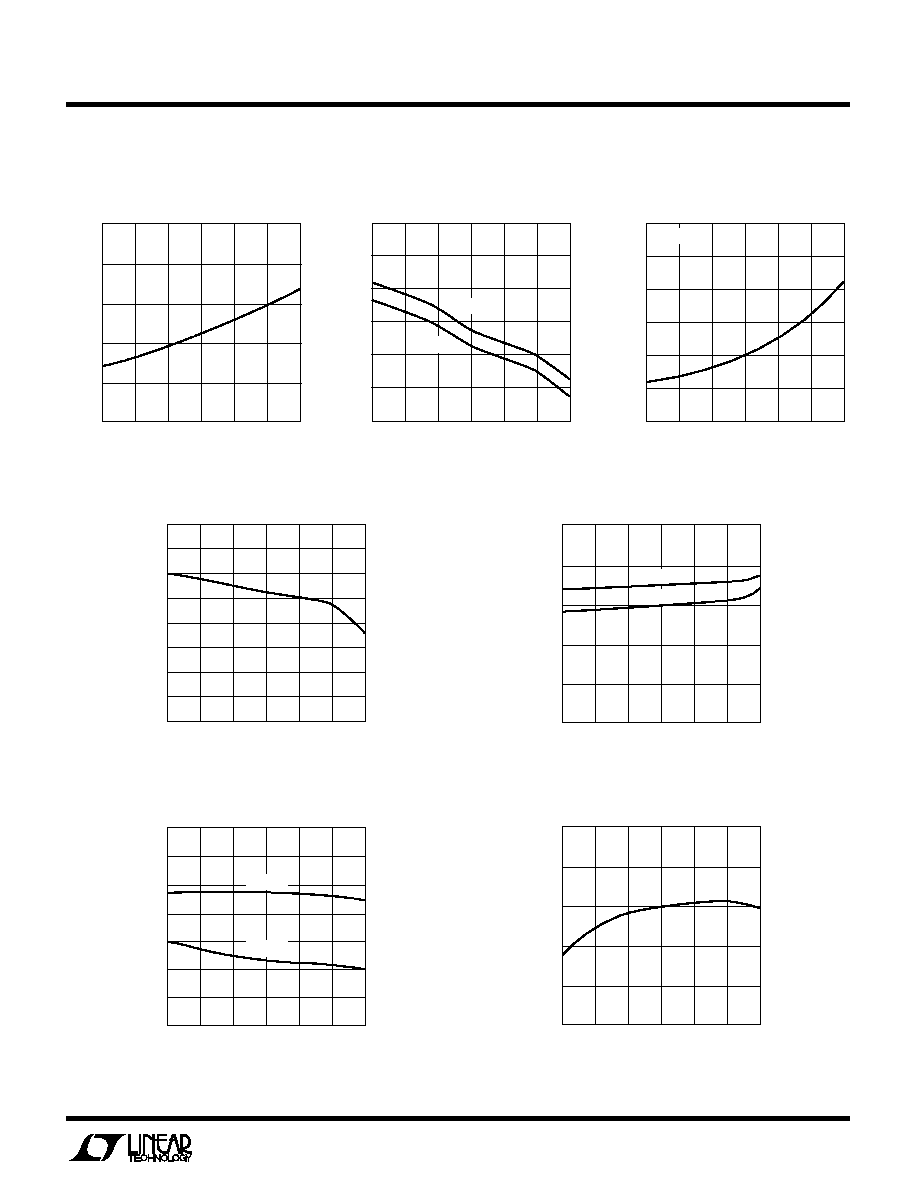
TYPICAL PERFOR
M
A
N
CE CHARACTERISTICS
U
W
TEMPERATURE (
°
C)
50
300
OSCILLATOR FREQUENCY (kHz) 400
500
600
700
800
25
0
25
50
1309 G01
75
100
Oscillator Frequency
TEMPERATURE (
°
C)
50
100
SWITCH SATURATION VOLTAGE (mV)
125
150
175
200
250
25
0
25
50
1309 G03
75
100
225
I
SW
= 500mA
TEMPERATURE (
°
C)
50
400
SWITCH CURRENT (mA)
500
600
700
800
1000
25
0
25
50
1309 G02
75
100
900
V
CC
= 3V
V
CC
= 5V
Switch Current Limit
Supply Current
TEMPERATURE (
°
C)
50
300
SUPPLY CURRENT (
µ
A)
400
500
600
700
800
25
0
25
50
1309 G05
75
100
V
CC
= 5V
V
CC
= 3V
Sense Voltage
TEMPERATURE (
°
C)
50
SENSE VOLTAGE (V)
11.95
12.00
12.05
25
75
1309 G04
11.90
11.85
11.80
25
0
50
12.10
12.15
12.20
100
Supply Current in Shutdown
Maximum Duty Cycle
TEMPERATURE (
°
C)
50
70
MAXIMUM DUTY CYCLE (%)
75
80
85
90
95
25
0
25
50
1309 G07
75
100
TEMPERATURE (
°
C)
50
8
10
12
25
75
1309 G06
6
4
25
0
50
100
2
0
SUPPLY CURRENT (
µ
A)
14
V
CC
= 5V
V
CC
= 3V
Switch Saturation Voltage
4
LT1309
TYPICAL PERFOR
M
A
N
CE CHARACTERISTICS
U
W
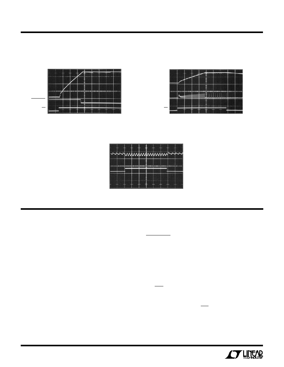
50
µ
s/DIV
1309 G08
12V
V
OUT
2V/DIV
V
ON/OFF
10V/DIV
VPP VALID
10V/DIV
Start-Up Waveforms, I
LOAD
= 10mA
Start-Up Waveforms, I
LOAD
= 1mA
50
µ
s/DIV
1309 G09
V
OUT
5V/DIV
V
ON/OFF
10V/DIV
I
L
500mA/DIV
12V OUTPUT
1V/DIV
AC COUPLED
10mA
60mA
I
LOAD
50
µ
s/DIV
1309 G10
PI FU CTIO S
U
U
U
SOFT START (Pin 1): A 0.1
µ
F/1M
parallel RC from this
pin to GND provides a Soft Start function upon device
turn-on. Initially about 80
µ
A will flow from the pin into the
capacitor. When the voltage at the pin reaches approxi-
mately 0.4V, current ceases flowing out of the pin.
V
CC
(Pin 2): Input Supply. At least 1
µ
F input bypass
capacitance is required. More capacitance reduces ring-
ing on the supply line.
PGND (Pin 3): Power Ground. Connect to ground plane.
V
SW
(Pin 4): Collector of Power Switch. High dV/dt
present on this pin. To minimize radiated noise keep
layout short and direct.
GND (Pin 5): Signal Ground. Connect to ground plane.
VPP VALID (Pin 6): This pin provides a logic signal
indicating that output voltage has reached 12V. Active low
with internal 200k pull-up resistor.
SENSE (Pin 7): Output Sense Pin. This pin connects to a
resistive divider that sets the output voltage. In shutdown,
the resistor string is disconnected and current into this pin
reduces to < 1
µ
A.
ON/OFF (Pin 8): Shutdown Control. When pulled below
1.5V, this pin disables the LT1309 and reduces supply
current to 9
µ
A. All circuitry is disabled in shutdown. The
part is enabled when ON/OFF is greater than 1.5V.
Load Transient Response,
C
OUT
= 1
µ
F
5
LT1309
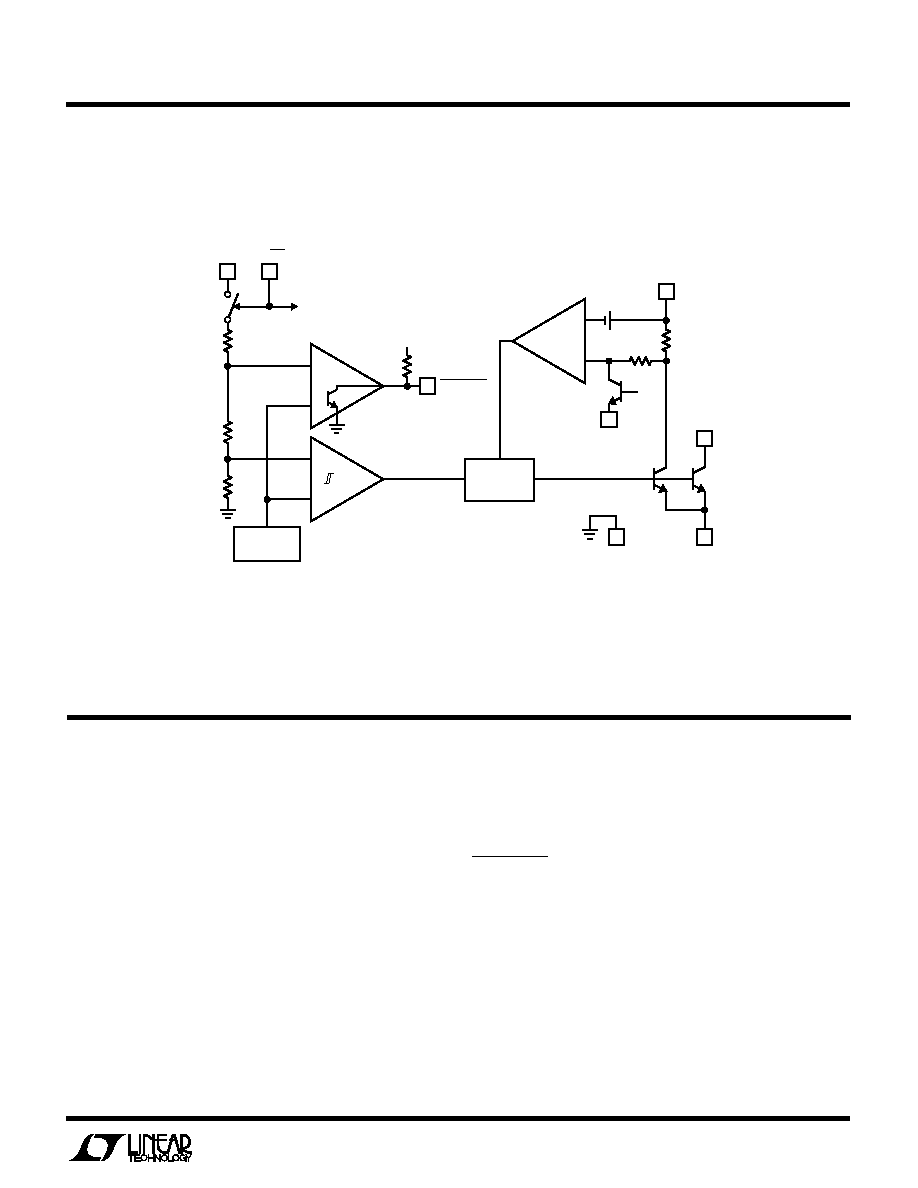
OPERATIO
U
The LT1309 is a current limited, Burst Mode (gated
oscillator) type switching regulator that produces a 12V
output from a 3.3V or 5V input. Operation can best be
understood by referring to the Block Diagram. When the
voltage at the Sense pin (Pin 7) is less than 12V, compara-
tor C1 enables the oscillator, turning switches Q1 and Q2
on. The switch turns off when current limit is reached or
when the oscillator maximum on-time is reached. When
Q2 turns off, current built up in the inductor flows into the
output capacitor and load. This action occurs until the
output voltage reaches 12V. During start-up, the Sense pin
voltage is either 3.3V or 5V, depending on the input. The
VPP VALID signal remains high until the output voltage
reaches 12V, signaling correct voltage level to program
flash memory. Connecting a 1
µ
F/0.1
µ
F parallel RC to the
Soft Start pin limits inrush current during start-up.
BLOCK DIAGRA
W
V
CC
8
ON/OFF
SENSE
7
4k
864k
200k
VPP VALID
OFF
Q3
Q2
×
1
Q1
×
50
100k
+
C2
V
REF
1.24V
R1
3
+
C3
36mV
V
CC
PGND
1309 BD
SW
R2
700
5
3
4
GND
1
SOFT START
BIAS
+
500kHz
OSCILLATOR
+
C1
2
POWER ON
6