 | ÐлекÑÑоннÑй компоненÑ: LT1310 | СкаÑаÑÑ:  PDF PDF  ZIP ZIP |
Äîêóìåíòàöèÿ è îïèñàíèÿ www.docs.chipfind.ru
1
LT1310
1310f
1.5A Boost
DC/DC Converter
with Phase-Locked Loop
The LT
®
1310 boost DC/DC converter combines a 1.5A
current mode PWM switcher with an integrated phase-
locked loop, allowing the user to set the switching fre-
quency anywhere from 10kHz to 4.5MHz. Intended for use
in applications where switching frequency must be accu-
rately controlled, the LT1310 can generate 12V at up to
400mA from a 5V input.
Switching frequency is set with an external capacitor, and
the device can be operated in either free-running or phase-
locked mode. A wide capture range of nearly 2:1 allows the
free-running frequency to be set using standard
±
10%
tolerance NP0 dielectric capacitors.
The LT1310 is available in the tiny thermally enhanced
10-lead MSOP package.
s
Synchronizable or Constant Frequency
Low Noise Output
s
Synchronizable Up to 4.5MHz
s
Wide Input Voltage Range: 2.8V to 18V
s
Low Profile Surface Mount Solution
(All Ceramic Capacitors)
s
Low V
CESAT
Switch: 240mV at 1A
s
Adjustable Output from V
IN
to 35V
s
Small Thermally Enhanced 10-Lead MSOP Package
s
Instruments
s
Avionics
s
Data Acquisition
s
Communications
s
Imaging
s
Ultrasound
, LTC and LT are registered trademarks of Linear Technology Corporation.
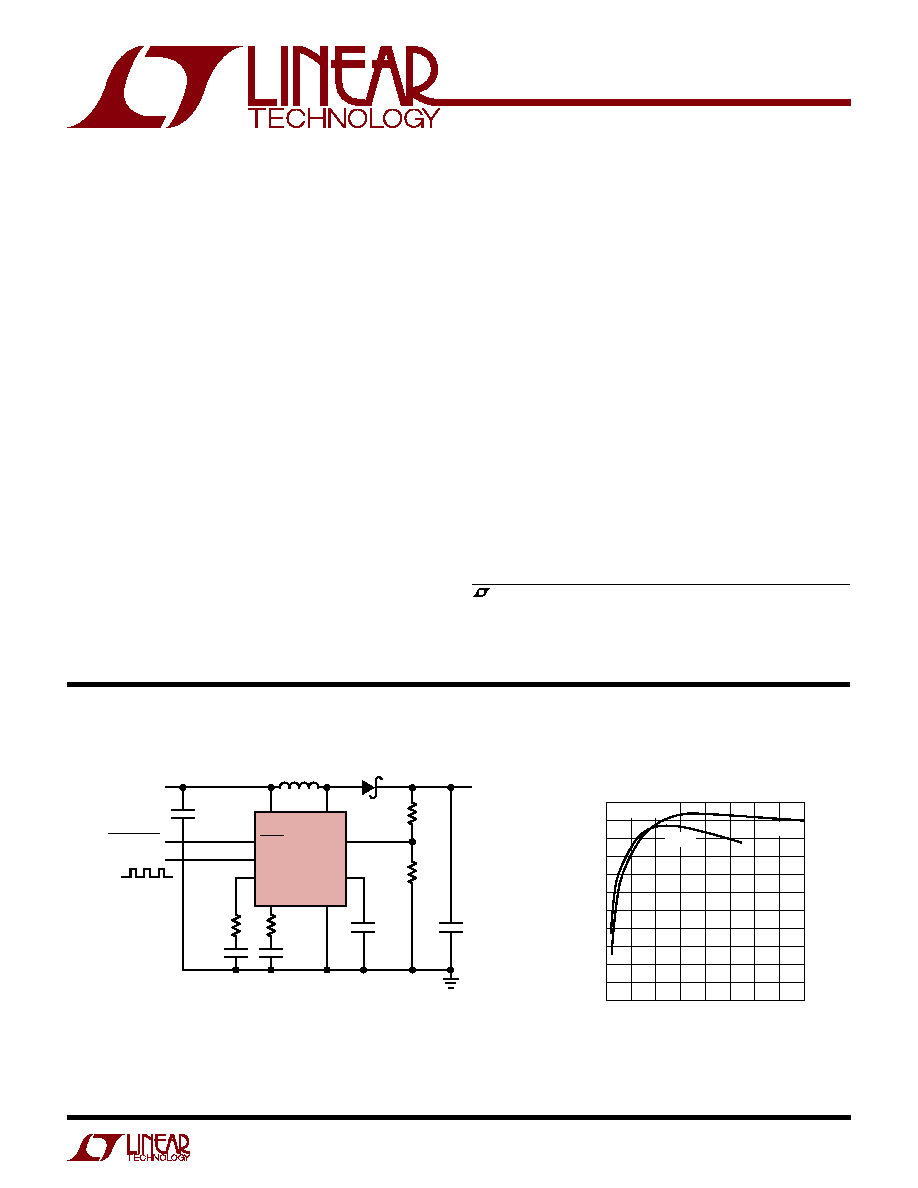
V
IN
SHDN
SHUTDOWN
SYNC
1.6MHz
SYNC
PLL-LPF
3.01k
V
IN
5V
15k
178k
20.5k
100pF
NP0
1310 F01a
C2
4.7
µ
F
CERAMIC
V
OUT
12V
400mA
1500pF
820pF
C1: 4.7
µ
F, X5R OR X7R, 6.3V
C2: 4.7
µ
F, X5R OR X7R, 16V
D1: MICROSEMI UPS120 OR EQUIVALENT
L1: PANASONIC ELL6SH-5R6M
*EXPOSED PAD MUST ALSO BE GROUNDED
C1
4.7
µ
F
CERAMIC
FB
C
T
V
C
SW
D1
LT1310
L1
5.6
µ
H
GND*
LOAD CURRENT (mA)
0
35
EFFICIENCY (%)
45
55
65
75
100
200
1310 F01b
400
300
85
40
50
60
70
80
90
3.3V
IN
V
OUT
= 12V
5V
IN
Figure 1. 5V to 12V Converter Synchronized at 1.6MHz
LT1310 Efficiency
DESCRIPTIO
U
FEATURES
APPLICATIO S
U
TYPICAL APPLICATIO
U
2
LT1310
1310f
PARAMETER
CONDITIONS
MIN
TYP
MAX
UNITS
Undervoltage Lockout
2.8
V
Maximum Input Voltage
18
V
Feedback Voltage
1.242
1.255
1.268
V
q
1.236
1.268
V
FB Pin Bias Current
60
150
nA
Reference Line Regulation
V
IN
= 2.9V to 18V
0.01
0.05
%/V
Error Amplifier Transconductance
I = 5
µ
A
350
µ
A/V
Error Amplifier Voltage Gain
200
V/V
SW Current Limit
1.5
2.1
2.8
A
SW Saturation Voltage
I
SW
= 1A
0.240
0.320
V
SW Maximum Duty Cycle
C
T
= 220pF
80
84
%
C
T
= 47pF
78
83
%
SW Minimum On Time
I
SW
= 150mA, V
C
= 0.25V
70
ns
VCO Frequency
C
T
= 220pF, PLL-LPF = High
0.950
1.10
1.25
MHz
C
T
= 220pF, PLL-LPF = High
q
0.800
1.30
MHz
C
T
= 220pF, PLL-LPF = Low
500
630
kHz
C
T
= 47pF, PLL-LPF = High
3.3
MHz
Frequency Foldback
C
T
= 220pF, PLL-LPF = High, FB = 0V
200
kHz
PLL Lock Range
C
T
= 220pF, Maximum
0.950
1.10
1.25
MHz
C
T
= 220pF, Minimum (Percent Change from Max)
40
50
%
Supply Current
SHDN = High
11.5
15
mA
SHDN = Low
1
µ
A
SW Leakage Current
Switch Off, SW = 3.3V
0.1
5
µ
A
SHDN Pin Bias Current
V
SHDN
= 2.4V
35
65
µ
A
SHDN Pin High
Active Mode
2.4
V
SHDN Pin Low
Shutdown Mode
0.4
V
(Note 1)
SW Voltage .............................................................. 36V
V
IN
Voltage ............................................................. 18V
SHDN Voltage ......................................................... 18V
SYNC Voltage ........................................................... 5V
FB Voltage ................................................................. 5V
C
T
Voltage ................................................................. 5V
V
C
Voltage ................................................................. 2V
PLL-LPF Pin Current ............................................... 1mA
Operating Temperature Range (Note 2) .. 40
°
C to 85
°
C
Storage Temperature Range ................. 65
°
C to 150
°
C
Lead Temperature (Soldering, 10 sec).................. 300
°
C
ORDER PART
NUMBER
LT1310EMSE
T
JMAX
= 125
°
C,
JA
= 40
°
C/W
EXPOSED PAD IS GROUND
(MUST BE SOLDERED TO PCB)
The
q
denotes specifications which apply over the full operating
temperature range, otherwise specifications are at T
A
= 25
°
C. V
IN
= 3.3V, V
SHDN
= 3.3V, unless otherwise noted. (Note 2)
1
2
3
4
5
FB
SHDN
PLL-LPF
SYNC
GND
10
9
8
7
6
V
C
C
T
V
IN
SW
SW
TOP VIEW
MSE EXPOSED PAD PACKAGE
10-LEAD PLASTIC MSOP
MSE PART MARKING
LTRZ
Consult LTC Marketing for parts specified with wider operating temperature ranges.
Note 1: Absolute Maximum Ratings are those values beyond which the life
of a device may be impaired.
Note 2: The LT1310E is guaranteed to meet performance specifications
from 0
°
C to 70
°
C. Specifications over the 40
°
C to 85
°
C operating
temperature range are assured by design, chacterization and correlation
with statistical process controls.
ABSOLUTE AXI U RATI GS
W
W
W
U
PACKAGE/ORDER I FOR ATIO
U
U
W
ELECTRICAL CHARACTERISTICS
3
LT1310
1310f
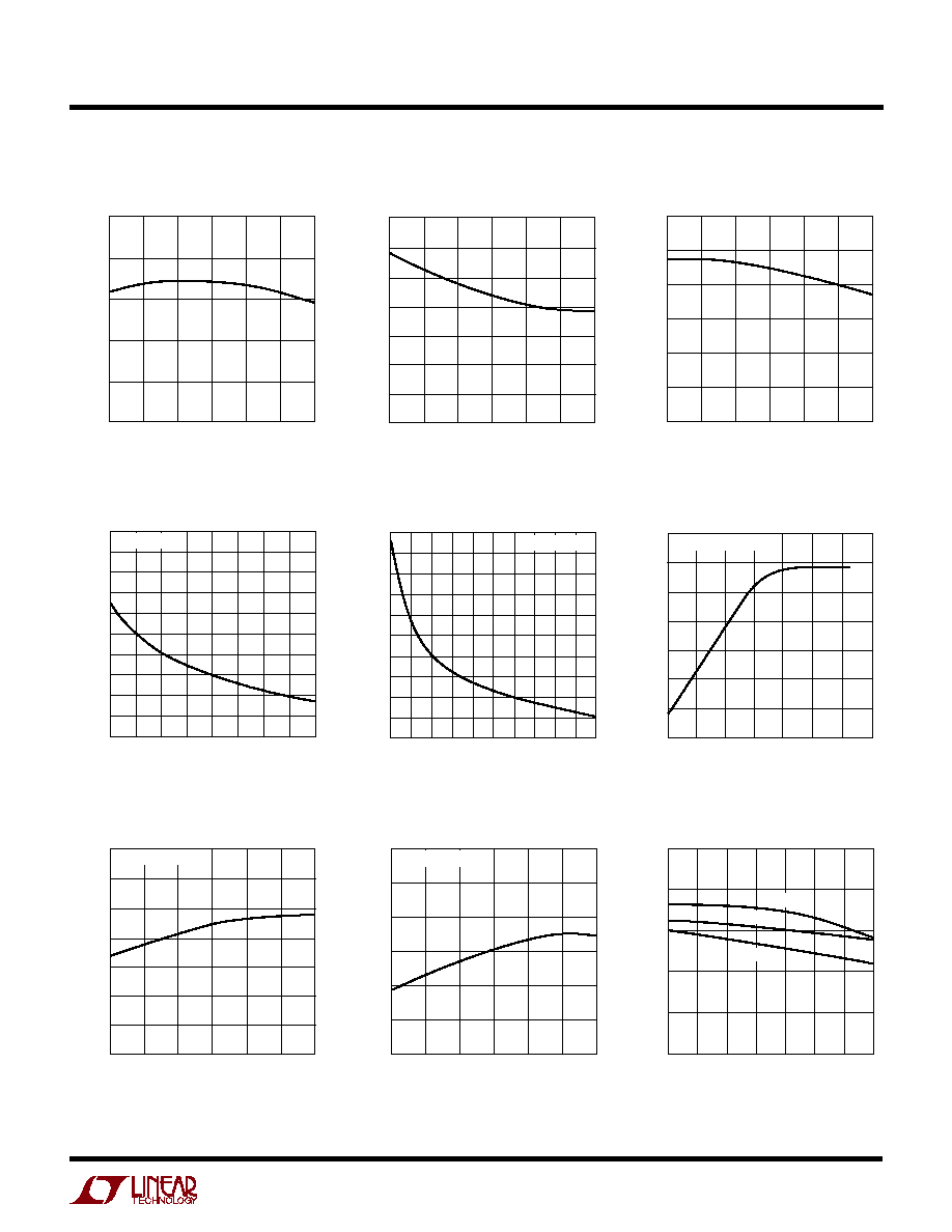
Feedback Voltage
TEMPERATURE (
°
C)
50
1.22
FB VOLTAGE (V)
1.23
1.24
1.25
1.26
1.27
25
0
25
50
1310 G01
75
100
TEMPERATURE (
°
C)
50
140
120
100
80
60
40
20
0
25
75
1310 G02
25
0
50
100
FEEDBACK CURRENT (nA)
TEMPERATURE (
°
C)
50
2.50
UNDERVOLTAGE LOCKOUT (V) 2.55
2.60
2.65
2.70
2.80
25
0
25
50
1310 G03
75
100
2.75
Feedback Pin Current
Undervoltage Lockout
Oscillator Frequency
vs C
T
Capacitor
CAPACITOR (pF)
20
1000
FREQUENCY (kHz)
3000
6000
40
60
LT1372 · G10
2000
5000
4000
80
100
PLL-LPF = HIGH
Oscillator Frequency
vs C
T
Capacitor
CAPACITOR (pF)
100
FREQUENCY (kHz)
1200
1600
2000
900
1310 G05
800
400
0
300
500
700
1100
PLL-LPF = HIGH
Oscillator Frequency
vs Feedback Voltage
FEEDBACK (V)
0
800
1000
1400
0.6
1.0
1310 G06
600
400
0.2
0.4
0.8
1.2
1.4
200
0
1200
FREQUENCY (kHz)
220pF C
T
CAPACITOR
Oscillator Frequency
220pF Capacitor on C
T
Pin
Maximum Duty Cycle
vs Oscillator Frequency
TEMPERATURE (
°
C)
50
1600
1400
1200
1000
800
600
400
200
25
75
1310 G07
25
0
50
100
FREQUENCY (kHz)
PLL-LPF = HIGH
Oscillator Frequency
47pF Capacitor on C
T
Pin
TEMPERATURE (
°
C)
50
2000
FREQUENCY (kHz)
2300
2600
2900
3200
3800
25
0
25
50
1310 G08
75
100
3500
PLL-LPF = HIGH
OSCILLATOR FREQENCY (kHz)
500 1000
50
MAX DUTY CYCLE (%)
70
100
1500
2500 3000
1310 G09
60
90
80
2000
3500 4000
100
°
C
25
°
C
50
°
C
TYPICAL PERFOR A CE CHARACTERISTICS
U
W
4
LT1310
1310f
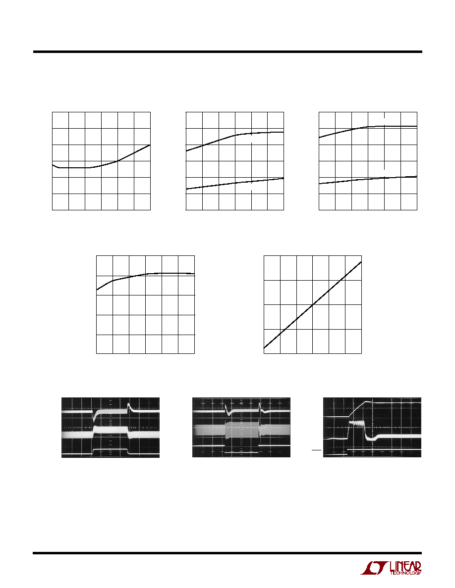
Switch Minimum On Time
PLL Lock Range
220pF Capacitor on C
T
Pin
Supply Current
Switch V
CESAT
TEMPERATURE (
°
C)
50
40
MINIMUM ON TIME (ns)
50
60
70
80
100
25
0
25
50
1310 G10
75
100
90
TEMPERATURE (
°
C)
50
200
FREQUENCY (kHz)
400
600
800
1000
1400
25
0
25
50
1310 G11
75
100
1200
MAXIMUM
MINIMUM
TEMPERATURE (
°
C)
50
500
FREQUENCY (kHz)
1000
1500
2000
2500
3500
25
0
25
50
1310 G12
75
100
3000
MAXIMUM
MINIMUM
PLL Lock Range
47pF Capacitor on C
T
Pin
TEMPERATURE (
°
C)
50
7
SUPPLY CURRENT (mA)
8
9
10
11
12
25
0
25
50
1310 G13
75
100
SWITCH CURRENT (A)
0
0
V
CESAT
(mV)
100
200
300
400
0.5
1.0
1310 G15
1.5
Transient Response
PLL Response
Start-Up Response
V
OUT
100mV/DIV
I
L
500mA/DIV
200mA
100mA
I
LOAD
f
SYNC
= 1.5MHz
50
µ
s/DIV
LT1310 G16
V
OUT
50mV/DIV
I
L
200mA/DIV
1.9MHz
1.2MHz
f
SYNC
50
µ
s/DIV
LT1310 G17
V
OUT
5V/DIV
I
L
1A/DIV
V
SHDN
NO SYNC SIGNAL 20
µ
s/DIV
LT1310 G18
f = 1.2MHz
TYPICAL PERFOR A CE CHARACTERISTICS
U
W
5
LT1310
1310f
FB (Pin 1): Feedback Pin for Error Amplifier. Connect the
resistor divider here to set output voltage according to
the formula:
V
OUT
= 1.255(1 + R1/R2)
FB
R1
V
OUT
R2
Minimize trace area at this pin.
SHDN (Pin 2): Shutdown Pin. For active mode, tie this pin
to a voltage between 2.4V and 18V. To disable the part and
go into low current mode, pull this pin below 0.4V.
PLL-LPF (Pin 3): Phase Locked-Loop Filter Pin. This is the
output of the phase detector and also the input to the
voltage controlled oscillator (VCO). Connect an RC filter
here. Typically, R = 3k and C = 1500pF. The voltage range
at the PLL-LPF pin is approximately 0V to 1.5V with 1.5V
corresponding to the maximum switching frequency. For
applications not requiring synchronization, use a pull-up
resistor at this pin; the pull-up voltage must be above 2.4V.
Set the pull-up resistor value according to:
R
V
V
A
PULLUP
PULLUP
=
(
)
µ
.
1 5
300
For a pull-up voltage of 5V:
R
V
V
A
k
PULLUP
=
(
)
µ
5
1 5
300
11 6
.
.
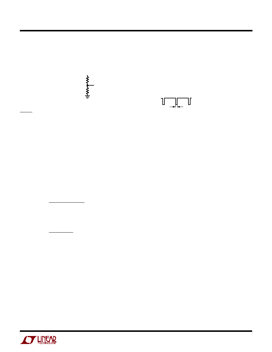
SYNC (Pin 4): Frequency Synchronization Pin. Inject the
external synchronizing signal here. The phase detector is
edge triggered and when locked the rising edge of the
sync signal will be aligned with the turn-on of the power
transistor. The SYNC signal must have a minimum HIGH
amplitude of 1.2V and a maximum LOW amplitude of
0.2V with the signal staying low for at least 100ns.
1.2V (MIN)
0.2V (MAX)
100ns (MIN)
GND (Pin 5, Exposed Pad): Ground. Tie both Pin 5 and
the exposed pad directly to local ground plane. The
ground metal to the exposed pad should be wide for better
heat dissipation. Multiple vias (local ground plane
ground backplane) placed close to the exposed pad can
further aid in reducing thermal resistance. The exposed
pad must be soldered to ground for the LT1310 to function
properly.
SW (Pins 6, 7): Switch Pin. Connect inductor/diode here.
Minimize trace area at this pin to keep EMI down.
V
IN
(Pin 8): Supply Pin. Must be bypassed as close as
possible to the pin.
C
T
(Pin 9): Timing Capacitor Pin for VCO. Place the timing
capacitor from this pin to ground to set the frequency
range for the oscillator. Minimize trace at this pin to reduce
stray capacitance.
V
C
(Pin 10): Compensation Pin for Error Amplifier. Tie an
RC network here to compensate the voltage feedback
loop.
U
U
U
PI FU CTIO S