 | ÐлекÑÑоннÑй компоненÑ: LT1319 | СкаÑаÑÑ:  PDF PDF  ZIP ZIP |
Äîêóìåíòàöèÿ è îïèñàíèÿ www.docs.chipfind.ru
1
LT1319
S
FEATURE
D
U
ESCRIPTIO
The LT
®
1319 is a general purpose building block that
contains all the circuitry necessary to transform modu-
lated photodiode signals back to digital signals. The
circuit's flexibility permits it to receive multiple modulation
methods. A low noise, high frequency preamplifier per-
forms a current-to-voltage conversion while rejecting low
frequency ambient interference with an AC coupling loop.
Two separate high impedance filter buffer inputs are
provided so that off-chip filtering can be tailored for
specific modulation schemes. The filter buffers drive sepa-
rate differential gain stages that end in comparators with
internal hysteresis. The comparator thresholds are adjust-
able externally by the current into Pin 11. One channel has
a high speed 25ns comparator required for high data rates.
The second channel's comparator has a 60ns response
time and is well suited to more modest data rates. A power
saving shutdown feature is useful in portable applications.
For IRDA 4PPM contact the LTC Marketing Department.
Multiple Modulation Standard
Infrared Receiver
s
Receives Multiple IR Modulation Methods
s
Low Noise, High Speed Preamp: 2pA/
Hz, 7MHz
s
Low Frequency Ambient Rejection Loops
s
Dual Gain Channels: 8MHz, 400V/V
s
25ns and 60ns Comparators
s
16-Lead SO Package
s
5V Single Supply Operation
s
Supply Current: 14mA
s
Shutdown Supply Current: 500
µ
A
s
External Comparator Threshold Setting
s
IRDA: SIR, FIR
s
Sharp/Newton
s
TV Remote
s
High Data Rate Modulation Methods
ODULATIO STA DARDS
U
U
W
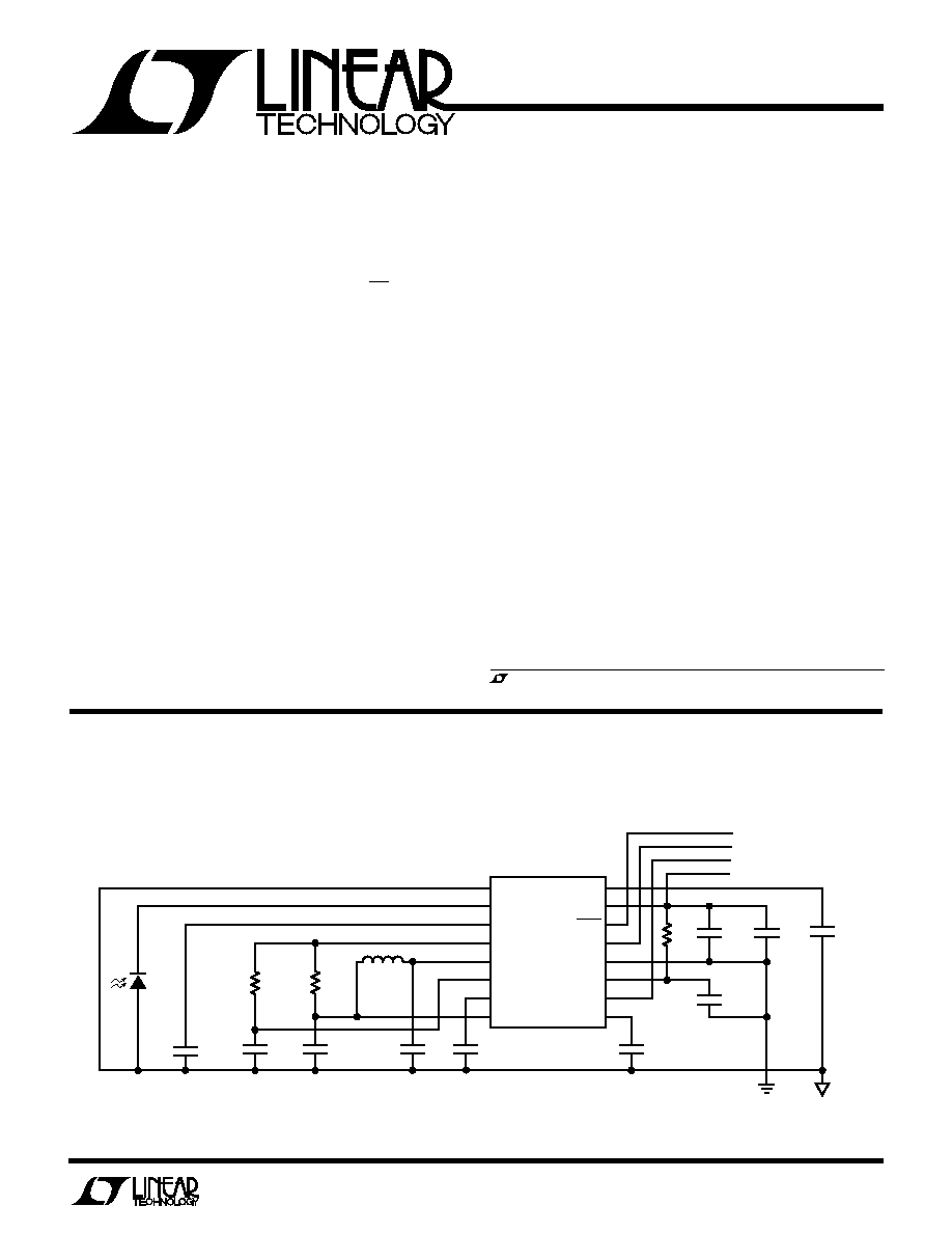
IRDA and Sharp/Newton Data Receiver
TYPICAL APPLICATIO
N
U
AN_GND
IN
FILT1
PREOUT
V
BIAS
FILTINL
FILT2L
FILTIN
LT1319
SHUTDOWN INPUT
IRDA DATA
SHARP/NEWTON DATA
V
CC
R
T1
30k
C
B1
0.1
µ
F
1
2
3
4
5
6
7
8
16
15
14
13
12
11
10
9
C
B3
10
µ
F
C
B2
10
µ
F
C
T1
1
µ
F
C
F4
2.2nF
C
B4
1
µ
F
L
F1
100
µ
H
C
F5
1
µ
F
AGND
DGND
LT1319 · TA01
C
F1
10nF
C
F3
100pF
C
F2
1nF
R
F2
2k
R
F1
1k
D1*
BYPASS
V
CC
SHDN
DATAL
DIG_GND
V
TH
DATA
FILT2
*BPW34FA OR BPV22NF
, LTC and LT are registered trademarks of Linear Technology Corporation.
2
LT1319
SYMBOL
PARAMETER
CONDITIONS
MIN
TYP
MAX
UNITS
V
OS
Preamp Input Offset Voltage
V (Pin 2) V (Pin 5)
4
15
mV
Preamp Output Offset Voltage
V (Pin 4) V (Pin 5)
10
25
mV
Preamp Loop Offset Voltage
V (Pin 3) V (Pin 5)
50
150
250
mV
High Gain Loop Offset Voltage
V (Pin 9) V (Pin 5)
600
800
950
mV
Low Gain Loop Offset Voltage
V (Pin 7) V (Pin 5)
600
800
950
mV
A
VP
Preamp Transimpedance
±
10
µ
A Into Pin 2, Measure
V (Pin 4), Fix Pin 3
10
15
17
k
Preamp Output Swing, Positive
100
µ
A Out of Pin 2, Measure
V (Pin 4), Fix Pin 3
0.25
0.4
0.55
V
Preamp Output Swing, Negative
100
µ
A Into Pin 2, Measure
V (Pin 4), Fix Pin 3
0.55
0.4
0.25
V
BW
P
Preamp Bandwidth
C (Pin 3) = 1
µ
F, Measure f
3dB
7
MHz
i
n
Preamp Input Noise Current
C (Pin 3) = 1
µ
F, f = 10kHz
2
pA/
Hz
Preamp Loop Rejection, Positive
50
µ
A Into Pin 2, Measure
V (Pin 4)
3
1
3
mV
Preamp Loop Rejection, Negative
50
µ
A Out of Pin 2, Measure
V (Pin 4)
3
1
3
mV
Preamp Loop Output Current, Positive
100
µ
A Out of Pin 2, Measure I (Pin 3), (Note 1)
150
100
50
µ
A
Preamp Loop Output Current, Negative
100
µ
A Into Pin 2, Measure I (Pin 3), (Note 1)
50
100
150
µ
A
V
BIAS
Bias Voltage
V (Pin 5)
1.7
1.9
2.1
V
V
BYPASS
Bypass Voltage
V (Pin 16)
4.75
4.9
4.95
V
I
B
Filter Buffer Input Bias Current
I (Pin 6), I (Pin 8)
0.1
0.5
1.4
µ
A
R
IN
Filter Buffer Input Resistance
V = 0.1V, Measure
I
B
Pin 6, Pin 8
40
M
Gain Stage Loop Rejection, Positive
V = 50mV (Pin 6, Pin 8), Measure
V (Pin 7, Pin 9)
0.33
0.45
0.57
V
Gain Stage Loop Rejection, Negative
V = 50mV (Pin 6, Pin 8), Measure
V (Pin 7, Pin 9)
0.57
0.45
0.33
V
A
VG
Gain Stages Voltage Gain
(Note 2)
400
V/V
BW
G
Gain Stages Bandwidth
C (Pin 7) = C (Pin 9) = 1
µ
F
8
MHz
t
r
Fast Comparator Response Time
10mV Overdrive
25
ns
Slow Comparator Response Time
10mV Overdrive
60
ns
V
HYS
Fast Comparator Hysteresis Voltage
(Note 3)
35
mV
Slow Comparator Hysteresis Voltage
(Note 3)
40
mV
V
OH
Fast Comparator Output High Voltage
V (Pin 9) = 200mV, 1mA Out of Pin 10 (Note 4)
2.4
3.5
V
Slow Comparator Output High Voltage
V (Pin 7) = 200mV, 0.1mA Out of Pin 13 (Note 4)
2.4
3.9
V
V
OL
Fast Comparator Output Low Voltage
V (Pin 9) = 200mV, 800
µ
A Into Pin 10
0.35
0.5
V
Slow Comparator Output Low Voltage
V (Pin 7) = 200mV, 800
µ
A Into Pin 13
0.39
0.5
V
A
U
G
W
A
W
U
W
A
R
BSOLUTE
XI
TI
S
W
U
U
PACKAGE/ORDER I FOR ATIO
ORDER PART
NUMBER
Total Supply Voltage (V
CC
to GND) ........................... 6V
Differential Voltage (Any Two Pins) .......................... 6V
Maximum Junction Temperature ......................... 150
°
C
Operating Temperature Range .................... 0
°
C to 70
°
C
Specified Temperature Range ..................... 0
°
C to 70
°
C
Storage Temperature Range ................ 65
°
C to 150
°
C
Lead Temperature (Soldering, 10 sec) ................. 300
°
C
LT1319CS
ELECTRICAL C
C
HARA TERISTICS
Consult factory for Industrial or Military grade parts.
T
A
= 25
°
C, V
15
= 5V, V
1
= V
12
= 0V, V
6
= V
8
= V
14
= 2V, unless otherwise specified.
T
JMAX
= 150
°
C,
JA
= 100
°
C/W
TOP VIEW
S PACKAGE
16-LEAD PLASTIC SO
1
2
3
4
5
6
7
8
16
15
14
13
12
11
10
9
AN_GND
IN
FILT1
PREOUT
V
BIAS
FILTINL
FILT2L
FILTIN
BYPASS
V
CC
SHDN
DATAL
DIG_GND
V
TH
DATA
FILT2
3
LT1319
SYMBOL
PARAMETER
CONDITIONS
MIN
TYP
MAX
UNITS
Threshold Transimpedance
100
µ
A Into Pin 11 (Note 5)
2
k
V
TH
Threshold External Voltage
100
µ
A Into Pin 11, V (Pin 11)
0.8
0.9
1.2
V
V
IH
Shutdown Input High Voltage
2
V
V
IL
Shutdown Input Low Voltage
0.8
V
I
IH
Shutdown Input High Current
V (Pin 14) = 2.4V
140
60
10
µ
A
I
IL
Shutdown Input Low Current
V (Pin 14) = 0.4V
400
260
130
µ
A
I
S
Supply Current
V (Pin 14) = 2V
10
14
18
mA
I
SHDN
Supply Current in Shutdown
V (Pin 14) = 0.8V, V (Pin 6) = V (Pin 8) = 0V
300
500
800
µ
A
ELECTRICAL C
C
HARA TERISTICS
T
A
= 25
°
C, V
15
= 5V, V
1
= V
12
= 0V, V
6
= V
8
= V
14
= 2V, unless otherwise specified.
0
°
C
T
A
70
°
C, V
15
= 5V, V
1
= V
12
= 0V, V
6
= V
8
= V
14
= 2V, unless otherwise specified.
SYMBOL
PARAMETER
CONDITIONS
MIN
TYP
MAX
UNITS
V
OS
Preamp Input Offset Voltage
V (Pin 2) V (Pin 5)
4
17
mV
Preamp Output Offset Voltage
V (Pin 4) V (Pin 5)
10
27
mV
Preamp Loop Offset Voltage
V (Pin 3) V (Pin 5)
30
150
350
mV
High Gain Loop Offset Voltage
V (Pin 9) V (Pin 5)
400
800
1200
mV
Low Gain Loop Offset Voltage
V (Pin 7) V (Pin 5)
400
800
1200
mV
A
VP
Preamp Transimpedance
±
10
µ
A Into Pin 2, Measure
V (Pin 4)
8.5
15
18.5
k
Preamp Output Swing, Positive
100
µ
A Out of Pin 2, Measure
V (Pin 4)
0.2
0.4
0.6
V
Preamp Output Swing, Negative
100
µ
A Into Pin 2, Measure
V (Pin 4)
0.6
0.4
0.2
V
Preamp Loop Rejection, Positive
50
µ
A Into Pin 2, Measure
V (Pin 4)
3.5
1
3.5
mV
Preamp Loop Rejection, Negative
50
µ
A Out of Pin 2, Measure
V (Pin 4)
3.5
1
3.5
mV
Preamp Loop Output Current, Positive
100
µ
A Out of Pin 2, Measure I (Pin 3), (Note 1)
160
100
40
µ
A
Preamp Loop Output Current, Negative
100
µ
A Into Pin 2, Measure I (Pin 3), (Note 1)
40
100
160
µ
A
V
BIAS
Bias Voltage
V (Pin 5)
1.5
1.9
2.3
V
V
BYPASS
Bypass Voltage
V (Pin 16)
4.7
4.9
4.97
V
I
B
Filter Buffer Input Bias Current
I (Pin 6), I (Pin 8)
0.05
0.5
1.6
µ
A
Gain Stage Loop Rejection, Positive
V = 50mV (Pin 6, Pin 8), Measure
V (Pin 7, Pin 9)
0.3
0.45
0.6
V
Gain Stage Loop Rejection, Negative
V = 50mV (Pin 6, Pin 8), Measure
V (Pin 7, Pin 9)
0.6
0.45
0.3
V
V
OH
Fast Comparator Output High Voltage
V (Pin 9) = 200mV, 1mA Out of Pin 10 (Note 4)
2.4
3.5
V
Slow Comparator Output High Voltage
V (Pin 7) = 200mV, 0.1mA Out of Pin 13 (Note 4)
2.4
3.9
V
V
OL
Fast Comparator Output Low Voltage
V (Pin 9) = 200mV, 800
µ
A Into Pin 10
0.35
0.5
V
Slow Comparator Output Low Voltage
V (Pin 7) = 200mV, 800
µ
A Into Pin 13
0.39
0.5
V
V
TH
Threshold External Voltage
100
µ
A Into Pin 11, V (Pin 11)
0.7
0.9
1.3
V
V
IH
Shutdown Input High Voltage
2
V
V
IL
Shutdown Input Low Voltage
0.8
V
I
IH
Shutdown Input High Current
V (Pin 14) = 2.4V
160
60
0
µ
A
I
IL
Shutdown Input Low Current
V (Pin 14) = 0.4V
450
260
80
µ
A
I
S
Supply Current
V (Pin 14) = 2V
9
14
20
mA
I
SHDN
Supply Current in Shutdown
V (Pin 14) = 0.8V, V (Pin 6) = V (Pin 8) = 0V
200
500
900
µ
A
Note 1: Measure V (Pin 3) without input current for Pin 2. Force Pin 3 to
this measured voltage (which disables the preamp loop). Measure the
current into and out of Pin 3 when Pin 2 is driven.
Note 2: The gain is the differential voltage at the comparator inputs divided
by the differential voltage between the filter buffer output and V
BIAS
. This
parameter is not tested.
Note 3: Hysteresis is the difference in comparator trip point measured
when the output is high and when the output is low. This parameter is
not tested.
Note 4: Measure V (Pin 7) and V (Pin 9). Force these voltages to 200mV
below their nominal value to switch the comparators high.
Note 5: The current into Pin 11 is multiplied by 4 and then applied to a
500
resistor on the positive comparator inputs. The threshold is
I (Pin 11) · 4 · 500
.
4
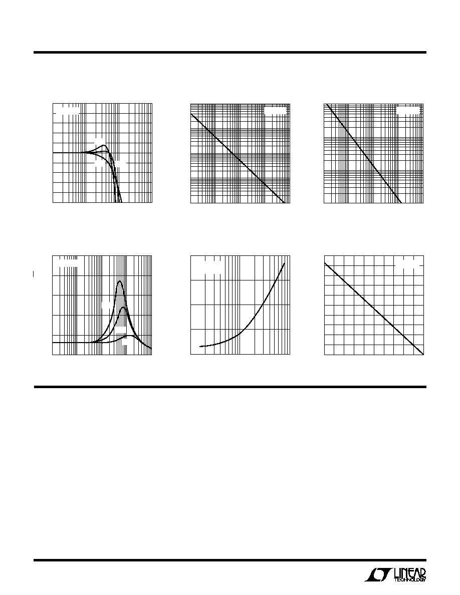
LT1319
TYPICAL PERFOR
M
A
N
CE CHARACTERISTICS
U
W
FREQUENCY (Hz)
100k
PREAMP OUTPUT/15k
(dB)
1M
10M
100M
1319 G01
5
4
3
2
1
0
1
2
3
4
5
T
A
= 25
°
C
50pF
30pF
10pF
Preamp Frequency Response vs
Input Capacitance
HIGHPASS CORNER FREQUENCY (Hz)
CAPACITANCE ON FILT2 (nF)
1k
100k
10k
1M
10M
1319 G03
1000
100
10
1
T
A
= 25
°
C
HIGHPASS CORNER FREQUENCY (Hz)
CAPACITANCE ON FILT1 (nF)
100
10k
100k
1M
1319 G02
1k
1000
100
10
1
0.1
T
A
= 25
°
C
Preamp Highpass vs
Capacitance on FILT1
Gain Stage Highpass vs
Capacitance on FILT2 or FILT2L
Preamp Output Noise vs
Input Capacitance
Input-Referred Noise vs
Lowpass Filter on PREOUT
FILTIN- or FILTINL-
Referred
Threshold Voltage vs R
T1
R
T1
(k
)
20
THRESHOLD VOLTAGE (mV)
1.0
0.9
0.8
0.7
0.6
0.5
1319 G06
30
40
T
A
= 25
°
C
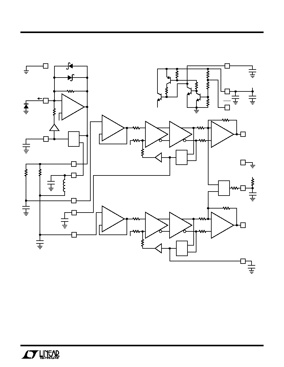
CIRCUIT DESCRIPTIO
U
The LT1319 is a general purpose low noise, high speed,
high gain, infrared receiver designed to easily provide IR
communications with portable computers, PDAs, desktop
computers and peripherals. The receiver takes the photo-
current from an infrared photodiode (Siemens BPW34FA
or Temic BPV22NF) and performs a current-to-voltage
conversion. After external filtering that is tailored for the
desired communication standard, two filter buffers are
provided. There are dual gain chains with nominal gain of
400V/V that feed internal comparators with hysteresis. The
comparator thresholds are set externally with a current into
the V
TH
pin. The high frequency comparator has a response
time of 25ns and is well-suited to high data rates.
The low frequency comparator responds in 60ns and is
useful for more modest data rates such as Sharp/Newton
and IRDA-SIR. The circuit also contains shutdown circuitry
to reduce power consumption. Rejection of ambient inter-
ference is accomplished with AC coupling loops around the
preamp and the two gain stages. The rejection frequency is
set with an internal resistor and an external capacitor to
ground. This feature allows changing of the break fre-
quency by simply switching in additional capacitors. To aid
in rejection of power supply noise there is internal supply
regulation and a fully differential topology after the filter
buffers.
FREQUENCY (Hz)
PREAMP OUTPUT NOISE (nV/
Hz)
250
200
150
100
50
0
10k
1M
10M
100M
1319 G04
100k
10pF
30pF
50pF
T
A
= 25
°
C
FILTER CUTOFF FREQUENCY (MHz)
0.1
INPUT CURRENT NOISE (nA r
ms)
20
15
10
5
0
1
10
1319 G05
T
A
= 25
°
C
R
FILTER
= 1k
5
LT1319
BLOCK DIAGRA
W
+
13
DATAL
5V
11
V
TH
12
DIG_GND
R
C1
500
R
G2
1k
R
L2
10k
V
BIAS
V
BIAS
g
m
4k
R
G1
1k
R
FB
15k
DS1
R
C2
500
R
SC
2k
LOW FREQUENCY
COMPARATOR
COMP 1
+
A3
A
V
= 20
+
A2
A
V
= 20
+
A1
FILTER
BUFFER
+
PREAMP
V
TH
GEN
R
L1
10k
R
F1
1k
R
F2
2k
R
T1
30k
C
T1
1
µ
F
R
H1
50k
R
S3
20k
R
S5
20k
R
S6
1k
R
S2
20k
R
S1
20k
R
S4
20k
R
H2
50k
1
GM2
GM3
+
10
DATA
R
C3
500
R
G4
1k
R
L3
10k
V
BIAS
g
m
4k
R
G3
1k
R
C4
500
HIGH FREQUENCY
COMPARATOR
COMP 2
+
A6
A
V
= 20
+
A5
A
V
= 20
+
A4
FILTER
BUFFER
1
+
+
+
+
g
m
4k
GM1
+
+
+
+
C
F1
10nF
C
B4
1
µ
F
C
F4
2.2nF
C
F2
1nF
+
+
+
C
F3
100pF
15
5V
V
CC
16
BYPASS
14
SHDN
C
B2
10
µ
F
+
+
+
C
B3
10
µ
F
+
C
B1
0.1
µ
F
C
F5
1
µ
F
9
FILT2
LT1319 · BD
Q1
Q2
Q4
V
REG
Q3
DS2
3
FILT1
6
FILTINL
7
FILT2L
8
FILTIN
5
V
BIAS
4
PREOUT
PHOTO-
DIODE
1
AN_GND
1
2
IN
IPD
L
F1
100
µ
H
+
NOTE: EXTERNAL COMPONENTS ARE SHOWN FOR AN IRDA AND SHARP/NEWTON DATA RECEIVER.