 | –≠–ª–µ–∫—Ç—Ä–æ–Ω–Ω—ã–π –∫–æ–º–ø–æ–Ω–µ–Ω—Ç: LT1339CN | –°–∫–∞—á–∞—Ç—å:  PDF PDF  ZIP ZIP |
1
LT1339
High Power Synchronous
DC/DC Controller
DESCRIPTIO
N
U
FEATURES
The LT
Æ
1339 is a high power synchronous current mode
switching regulator controller. The IC drives dual
N-channel MOSFETs to create a single IC solution for high
power DC/DC converters in applications up to 60V.
The LT1339 incorporates programmable average current
limiting, allowing accurate limiting of DC load current
independent of inductor ripple current. The IC also incor-
porates user-adjustable slope compensation for minimi-
zation of magnetics at duty cycles up to 90%.
The LT1339 timing oscillator operating frequency is pro-
grammable and can be synchronized up to 150kHz. Mini-
mum off-time operation provides main switch protection.
The IC also incorporates a soft start feature that is gated by
both shutdown and undervoltage lockout conditions.
An output phase reversal pin allows flexibility in configu-
ration of converter types, including inverting and negative
topologies.
s
High Voltage: Operation Up to 60V
s
High Current: Dual N-Channel Synchronous Drive
Handles Up to 10,000pF Gate Capacitance
s
Programmable Average Load Current Limiting
s
5V Reference Output with 10mA External
Loading Capability
s
Programmable Fixed Frequency Synchronizable
Current Mode Operation Up to 150kHz
s
Undervoltage Lockout with Hysteresis
s
Programmable Start Inhibit for Power Supply
Sequencing and Protection
s
Adaptive Nonoverlapping Gate Drive Prevents
Shoot-Through
s
48V Telecom Power Supplies
s
Personal Computers and Peripherals
s
Distributed Power Converters
s
Industrial Control Systems
s
Lead-Acid Battery Backup Systems
s
Automotive and Heavy Equipment
APPLICATIO
N
S
U
TYPICAL APPLICATIO
N
U
, LTC and LT are registered trademarks of Linear Technology Corporation.
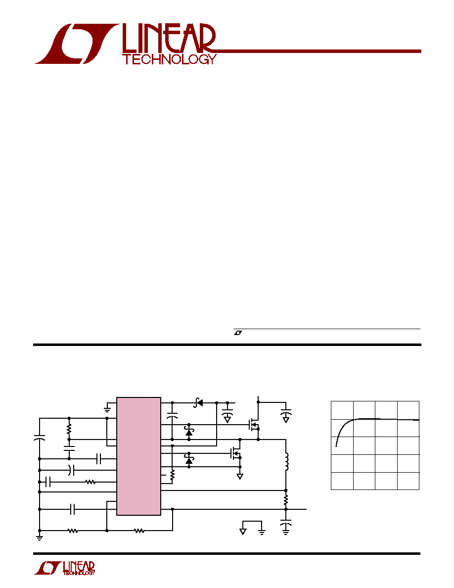
28V to 5V 20A Buck Converter
SYNC
V
BOOST
5V
REF
TG
CT
TS
SL/ADJ
12V
IN
I
AVG
BG
SS
PGND
V
C
PHASE
SGND
RUN/SHDN
V
FB
SENSE
+
V
REF
SENSE
≠
DBST
IN5819
12V
V
IN
28V
C
IN
1500
µ
F
63V
◊
3
IRL3803
IRL3103D2
◊
2
L1
10
µ
H
V
OUT
5V AT 20A
R
FB2
1k
R
FB1
3k
LT1339
+
CBST
1
µ
F
+
C
12VIN
47
µ
F
+
C
OUT
2200
µ
F
6.3V
◊
2
+
D2
MBR0520
D1
MBR0520
R
RUN
100k
R
S
0.005
R
CT
10k
C
CT
2200pF
C
AVG
2200pF
C
SS
,
1
µ
F
C
VC
,
1nF
R
VC
, 10k
C
REF
0.1
µ
F
1339 TA03
L1 = CTX02-13400-X2
C
5VREF
1
µ
F
+
+
28V to 5V Efficiency
OUTPUT CURRENT (A)
0
EFFICIENCY (%)
20
1339 TA03a
5
10
15
100
90
80
70
60
50
2
LT1339
A
U
G
W
A
W
U
W
A
R
BSOLUTE
XI
TI
S
12V
IN
= V
BOOST
= 12V, V
C
= 2V, TS = 0V, V
FB
= V
REF
= 1.25V, C
TG
= C
BG
= 3000pF, T
A
= 25
∞
C unless otherwise noted.
ELECTRICAL C
C
HARA TERISTICS
SYMBOL
PARAMETER
CONDITIONS
MIN
TYP
MAX
UNITS
Supply and Protection
I
12VIN
DC Active Supply Current (Note 2)
q
14
20
mA
DC Standby Supply Current
V
RUN/SHDN
< 0.5V
q
150
250
µ
A
I
BOOST
DC Active Supply Current (Note 2)
2.2
mA
DC Standby Supply Current
V
RUN/SHDN
< 0.5V
0
µ
A
V
RUN/SHDN
Shutdown Rising Threshold
q
1.15
1.25
1.35
V
V
SSHYST
Shutdown Threshold Hysteresis
25
mV
I
SS
Soft Start Charge Current
q
4
8
14
µ
A
V
UVLO
Undervoltage Lockout Threshold - Falling
q
8.20
9.00
9.75
V
Undervoltage Lockout Threshold - Rising
q
9.35
9.95
V
Undervoltage Lockout Hysteresis
q
200
350
mV
5V Reference
V
REF5
5V Reference Voltage
Line, Load and Temperature
q
4.75
5.00
5.25
V
5V Reference Line Regulation
10V
12V
IN
15V
q
3
5
mV/V
I
REF5
5V Reference Load Range - DC
q
10
mA
Pulse
q
20
mA
5V Reference Load Regulation
0
I
REF5
20mA
q
≠ 1.25
≠ 2
V/A
I
SC
5V Reference Short-Circuit Current
45
mA
Supply Voltages
Power Supply Voltage (12V
IN
) ...............≠ 0.3V to 20V
Topside Supply Voltage (V
BOOST
)
V
TS
≠ 0.3V to V
TS
+ 20V (V
MAX
= 75V)
Topside Reference Pin Voltage (TS) ......≠ 0.3V to 60V
Input Voltages
Sense Amplifier Input Common Mode ...≠ 0.3V to 60V
RUN/SHDN Pin Voltage ...................... ≠ 0.3V to 12V
IN
All Other Inputs ....................................... ≠ 0.3V to 7V
Maximum Currents
5V Reference Output Current............................ 65mA
Maximum Temperatures
Operating Ambient Temperature Range
LT1339C............................................. 0
∞
C to 70
∞
C
LT1339I ......................................... ≠ 40
∞
C to 85
∞
C
Storage Temperature Range ................. ≠ 65
∞
C to 150
∞
C
Lead Temperature (Soldering, 10 sec).................. 300
∞
C
(Note 1)
ORDER PART
NUMBER
LT1339CN
LT1339CSW
LT1339IN
LT1339ISW
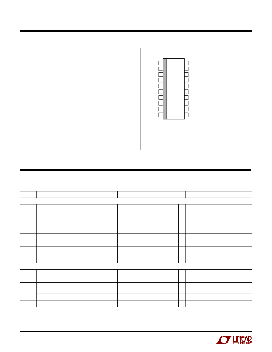
TOP VIEW
N PACKAGE
20-LEAD PDIP
SW PACKAGE
20-LEAD PLASTIC SO WIDE
1
2
3
4
5
6
7
8
9
10
20
19
18
17
16
15
14
13
12
11
SYNC
5V
REF
CT
SL/ADJ
I
AVG
SS
V
C
SGND
V
FB
V
REF
V
BOOST
TG
TS
12V
IN
BG
PGND
PHASE
RUN/SHDN
SENSE
≠
SENSE
+
W
U
U
PACKAGE/ORDER I FOR ATIO
T
JMAX
= 125
∞
C,
JA
= 70
∞
C/W (N)
T
JMAX
= 125
∞
C,
JA
= 85
∞
C/W (SW)
Consult factory for Military grade parts.
3
LT1339
12V
IN
= V
BOOST
= 12V, V
C
= 2V, TS = 0V, V
FB
= V
REF
= 1.25V, C
TG
= C
BG
= 3000pF, T
A
= 25
∞
C unless otherwise noted.
ELECTRICAL C
C
HARA TERISTICS
SYMBOL
PARAMETER
CONDITIONS
MIN
TYP
MAX
UNITS
Error Amplifier
V
FB
Error Amplifier Reference Voltage
Measured at Feedback Pin
1.242
1.250
1.258
V
q
1.235
1.250
1.265
V
I
FB
Feedback Input Current
V
FB
= V
REF
q
0.1
0.5
1.0
µ
A
g
m
Error Amplifier Transconductance
q
1200
2000
3200
µ
mho
A
V
Error Amplifier Voltage Gain
q
1500
3000
V/V
I
VC
Error Amplifier Source Current
q
200
275
µ
A
Error Amplifier Sink Current
V
FB
≠ V
REF
= 500mV
q
280
400
µ
A
V
VC
Absolute V
C
Clamp Voltage
Measured at V
C
Pin
3.5
V
V
SENSE
Peak Current Limit Threshold
Measured at Sense Inputs
q
170
190
mV
Average Current Limit Threshold (Note 4)
Measured at Sense Inputs
q
110
120
130
mV
V
IAVG
Average Current Limit Threshold
Measured at I
AVG
Pin
2.5
V
Current Sense Amplifier
A
V
Amplifier DC Gain
Measured at I
AVG
Pin
15
V/V
V
OS
Amplifier Input Offset Voltage
2V < V
CMSENSE
< 60V,
q
0.1
mV
SENSE
+
≠ SENSE
≠
= 5mV
I
B
Input Bias Current
Sink (V
CMSENSE
> 5V)
q
45
75
µ
A
Source (V
CMSENSE
= 0V)
q
700
1200
µ
A
Oscillator
f
O
Operating Frequency, Free Run
q
150
kHz
Frequency Programming Error (Note 3)
f
O
150kHz
q
≠ 5
5
%
I
CT
Timing Capacitor Discharge Current
LT1339C
q
2.20
2.50
2.75
mA
LT1339I
q
2.10
2.50
2.75
mA
V
SYNC
SYNC Input Threshold
Rising Edge
q
0.8
2.0
V
f
SYNC
SYNC Frequency Range
f
SYNC
150kHz
q
f
O
1.4f
O
Output Drivers
V
TG,BG
Undervoltage Output Clamp
12V
IN
8V
q
0.4
0.7
V
Standby Mode Output Clamp
V
RUN
< 0.5V
q
0.1
V
V
TG
Top Gate On Voltage
q
11.0
11.9
12.0
V
Top Gate Off Voltage
q
0.4
0.7
V
t
TGR
Top Gate Rise Time
q
130
200
ns
t
TGF
Top Gate Fall Time
q
60
140
ns
V
BG
Bottom Gate On Voltage
q
11.0
11.9
12.0
V
Bottom Gate Off Voltage
q
0.4
0.7
V
t
BGR
Bottom Gate Rise Time
q
70
200
ns
t
BGF
Bottom Gate Fall Time
q
60
140
ns
Note 2: Supply current specification does not include external FET gate
charge currents. Actual supply currents will be higher and vary with
operating frequency, operating voltages and the type of external FETs
used. See Application Information section.
Note 3: Test condition: R
CT
= 16.9k, C
CT
= 1000pF.
Note 4: Test Condition: V
CMSENSE
= 10V.
The
q
denotes specifications which apply over the full operating
temperature range.
Note 1: Absolute maximum ratings are those values beyond which the life
of a device may be impaired.
4
LT1339
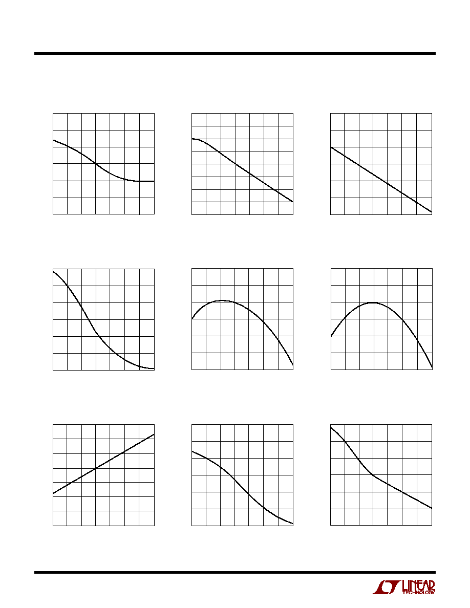
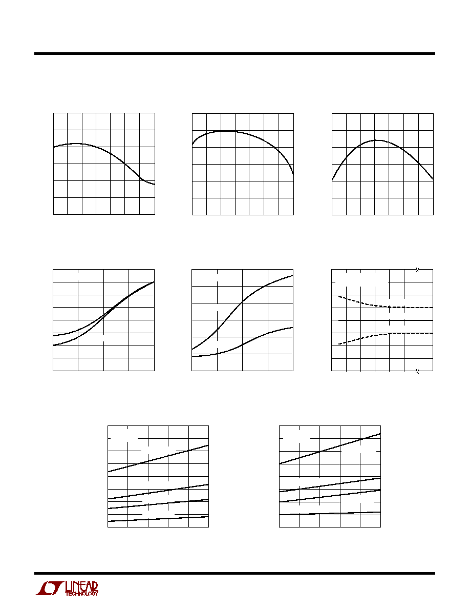
TYPICAL PERFOR
M
A
N
CE CHARACTERISTICS
U
W
TEMPERATURE (
∞
C)
≠50
BOOST SUPPLY CURRENT (mA)
4.0
3.5
3.0
2.5
2.0
1.5
1.0
25
75
1339 G01
≠25
0
50
100
125
Boost Supply Current vs
Temperature
TEMPERATURE (
∞
C)
≠50
5V REFERENCE SHORT-CIRCUIT CURRENT (mA)
60
55
50
45
40
35
30
25
75
1339 G03
≠25
0
50
100
125
TEMPERATURE (
∞
C)
≠50
I
12VIN
SUPPLY CURRENT (mA)
100
1339 G02
0
50
18
17
16
15
14
13
12
11
10
≠25
25
75
125
12V
IN
Supply Current vs
Temperature
5V Reference Short-Circuit
Current vs Temperature
I
12VIN
Shutdown Current vs
Temperature
Reference Voltage vs
Temperature
5V Reference Voltage vs
Temperature
TEMPERATURE (
∞
C)
≠50
I
12VIN
SHUTDOWN CURRENT (
µ
A)
190
180
170
160
150
140
130
25
75
1339 G04
≠25
0
50
100
125
TEMPERATURE (
∞
C)
≠50
REFERENCE VOLTAGE (V)
1.252
1.251
1.250
1.249
1.248
1.247
1.246
25
75
1339 G05
≠25
0
50
100
125
TEMPERATURE (
∞
C)
≠50
5V REFERENCE VOLTAGE (V)
5.01
5.00
4.99
4.98
25
75
1339 G06
≠25
0
50
100
125
TEMPERATURE (
∞
C)
≠50
4.5
4.0
3.5
3.0
2.5
2.0
1.5
1.0
25
75
1339 G07
≠25
0
50
100
125
ERROR AMPLIFIER VOLTAGE GAIN (kV/V)
TEMPERATURE (
∞
C)
≠50
ERROR AMPLIFIER TRANSCONDUCTANCE (m )
2.6
2.4
2.2
2.0
1.8
1.6
1.4
25
75
1339 G08
≠25
0
50
100
125
TEMPERATURE (
∞
C)
≠50
ERROR AMPLIFIER SOURCE CURRENT (
µ
A)
350
325
300
275
250
225
200
25
75
1339 G09
≠25
0
50
100
125
Error Amplifier Voltage Gain vs
Temperature
Error Amplifier Transconductance
vs Temperature
Error Amplifier Maximum Source
Current vs Temperature
5
LT1339
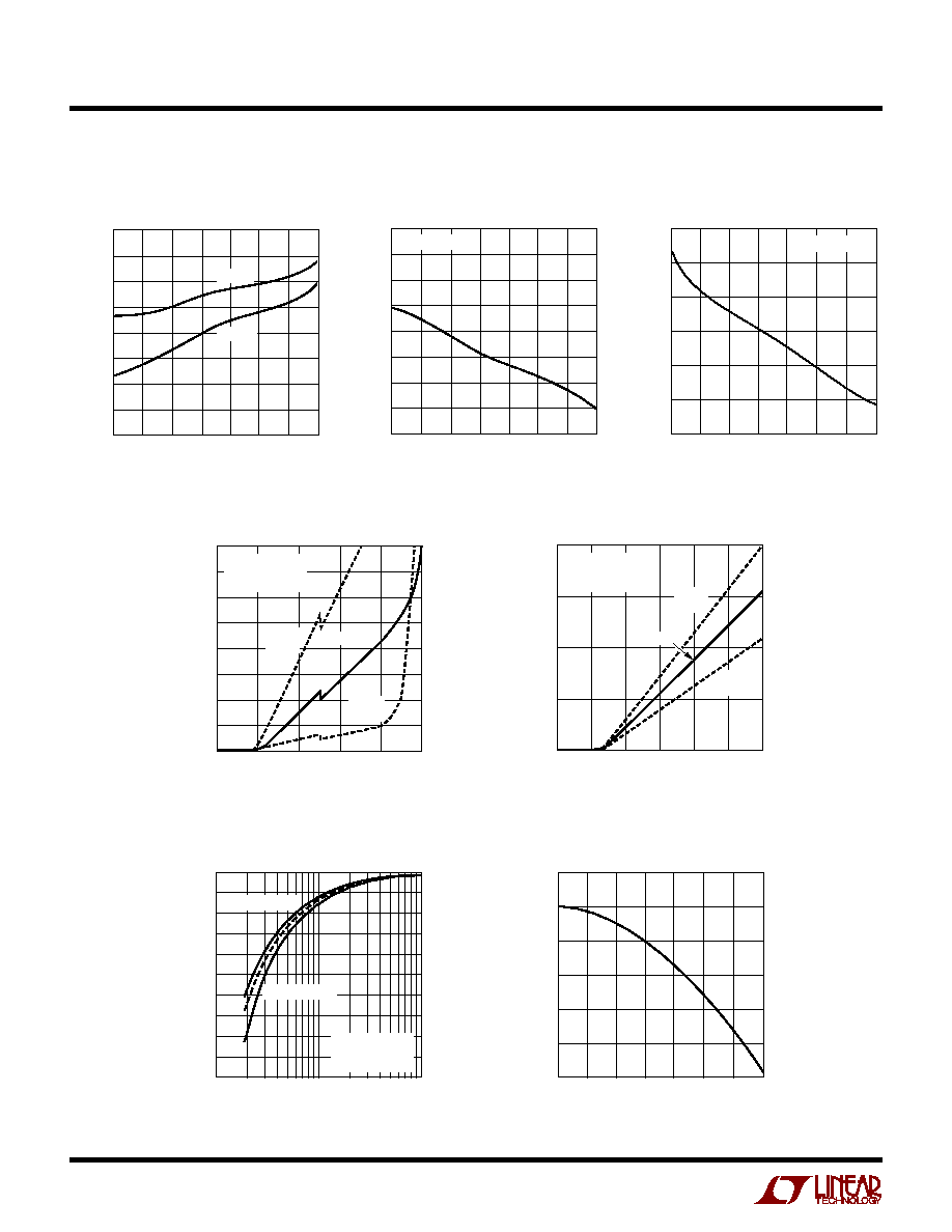
TYPICAL PERFOR
M
A
N
CE CHARACTERISTICS
U
W
TEMPERATURE (
∞
C)
≠50
SOFT START CHARGE CURRENT (
µ
A)
9
8
7
6
25
75
1339 G10
≠25
0
50
100
125
Soft Start Charge Current
vs Temperature
RUN/SHDN Threshold Hysteresis
vs Temperature
TEMPERATURE (
∞
C)
≠50
RUN/SHDN THRESHOLD HYSTERESIS (mV)
26
25
24
23
22
21
20
25
75
1339 G12
≠25
0
50
100
125
TEMPERATURE (
∞
C)
≠50
RUN/SHDN RISING THRESHOLD (V)
1.26
1.25
1.24
1.23
1.22
1.21
1.20
25
75
1339 G11
≠25
0
50
100
125
RUN/SHDN Rising Threshold
vs Temperature
BOTTOM GATE CAPACITANCE (pF)
1000
BOTTOM GATE TRANSITION TIMES (ns)
10000
1339 G13
2500
5000
7500
160
140
120
100
80
60
40
20
0
FALL TIME
RISE TIME
T
A
= 25
∞
C
Bottom Gate Transition Times vs
Bottom Gate Capacitance
Top Gate Transition Times vs
Top Gate Capacitance
TOP GATE CAPACITANCE (pF)
1000
TOP GATE TRANSITION TIMES (ns)
10000
1339 G14
2500
5000
7500
300
250
200
150
100
50
0
FALL TIME
RISE TIME
T
A
= 25
∞
C
V
SENSE(CM)
(V)
0
V
SENSE
(mV)
4
5
60
1339 G15
1
2
3
160
150
140
130
120
110
100
90
80
UPPER LIMIT
FULL OPERATING
TEMPERATURE RANGE
TYPICAL
LOWER LIMIT
Average Current Limit Threshold
Sense Voltage Tolerance vs
Common Mode Voltage
12V
IN
Supply Current vs
Supply Voltage
12V
IN
SUPPLY VOLTAGE (V)
10
12V
IN
SUPPLY CURRENT (mA )
15
14
1339 G16
11
12
13
30
28
26
24
22
20
18
16
14
C
BG
= 1000pF
C
BG
= 3300pF
C
BG
= 4700pF
C
BG
= 10000pF
f
O
= 100kHz
T
A
= 25
∞
C
Boost Supply Current vs
12V
IN
Supply Voltage
12V
IN
SUPPLY VOLTAGE (V)
10
BOOST SUPPLY CURRENT (mA )
15
14
1339 G17
11
12
13
18
16
14
12
10
8
6
4
2
C
TG
= 1000pF
C
TG
= 3300pF
C
TG
= 4700pF
C
TG
= 10000pF
f
O
= 100kHz
T
A
= 25
∞
C
6
LT1339
TEMPERATURE (
∞
C)
≠50
OPERATING FREQUENCY (NORMALIZED)
1.01
1.00
0.99
0.98
25
75
1339 G24
≠25
0
50
100
125
TYPICAL PERFOR
M
A
N
CE CHARACTERISTICS
U
W
TEMPERATURE (
∞
C)
≠50
I
B(SINK)
(
µ
A)
60
55
50
45
40
35
30
25
75
1339 G20
≠25
0
50
100
125
V
CMSENSE
= 10V
Sense Amplifier Input Bias
Current (Sink) vs Temperature
UVLO Thresholds vs Temperature
Sense Amplifier Input Bias
Current (Source) vs Temperature
RUN/SHDN INPUT VOLTAGE (V)
0
RUN/SHDN INPUT CURRENT (nA )
2.5
2.0
1339 G22
0.5
1.0
1.5
(1.25)
800
700
600
500
400
300
200
100
0
..................................................................
TYPICAL
UPPER
LIMIT
FULL OPERATING
TEMPERATURE
RANGE
LOWER
LIMIT
RUN/SHDN Input Current
vs Pin Voltage
Operating Frequency (Normalized)
vs Temperature
TEMPERATURE (
∞
C)
≠50
V
12VIN
(V)
100
1339 G18
0
50
10.00
9.75
9.50
9.25
9.00
8.75
8.50
8.25
8.00
≠25
25
75
125
RISING
FALLING
RUN/SHDN SUPPLY VOLTAGE (V)
0
RUN/SHDN INPUT CURRENT (
µ
A)
600
450
300
150
0
2
4
6
8
1339 G23
10
12
UPPER
LIMIT
LOWER
LIMIT
TYPICAL
FULL OPERATING
TEMPERATURE
RANGE
RUN/SHDN Input Current
vs Pin Voltage
Maximum Duty Cycle vs R
CT
R
CT
(k
)
1
2
4
6
MAXIMUM DUTY CYCLE (%)
100
90
80
70
60
50
40
30
20
10
0
10
20
40 60
100
1339 G21
I
DISCHG
= 2.1mA
I
DISCHG
= 2.75mA
FULL OPERATING
TEMPERATURE
RANGE
TEMPERATURE (
∞
C)
≠50
I
B(SOURCE)
(
µ
A)
100
1339 G19
0
50
1200
1100
1000
900
800
700
600
500
400
≠25
25
75
125
V
CMSENSE
= 0V

7
LT1339
SYNC (Pin 1): Oscillator Synchronization Pin with TTL-
Level Compatible Input. Input drives internal rising edge
triggered one-shot; sync signal on/off times should be
1
µ
s (10% to 90% DC at 100kHz). Does not contain
internal pull-up. Connect to SGND if not used.
5V
REF
(Pin 2): 5V Output Reference. Allows connection
of external loads up to 10mA DC. (Reference is not
available in shutdown.) Typically bypassed with 1
µ
F
capacitor to SGND.
CT (Pin 3): Oscillator Timing Pin. Connect a capacitor
(C
CT
) to ground and a pull-up resistor (R
CT
) to the 5V
REF
supply. Typical values are CT = 1000pF and 10k
R
CT
30k.
SL/ADJ (Pin 4): Slope Compensation Adjustment.
Allows increased slope compensation for certain high
duty cycle applications. Resistive loading of the pin
increases effective slope compensation. A resistor
divider from the 5V
REF
pin can tailor the onset of addi-
tional slope compensation to specific regions in each
switch cycle. Pin can be floated or connected to 5V
REF
if
no additional slope compensation is required. (See
Applications Information section for slope compensa-
tion details.)
I
AVG
(Pin 5): Average Current Limit Integration. Fre-
quency response characteristic is set using the 50k
output impedance and external capacitor to ground.
Averaging roll-off typically set at 1 to 2 orders of magni-
tude under switching frequency. (Typical capacitor value
~1000pF for f
O
= 100kHz.) Shorting this pin to SGND will
disable the average current limit function.
SS (Pin 6): Soft Start. Generates ramping threshold for
regulator current limit during start-up and after UVLO
event by sourcing about 8
µ
A into an external capacitor.
V
C
(Pin 7): Error Amplifier Output. RC load creates
dominant compensation in power supply regulation feed-
back loop to provide optimum transient response. (See
Applications Information section for compensation de-
tails.)
SGND (Pin 8): Small-Signal Ground. Connect to negative
terminal of C
OUT
.
V
FB
(Pin 9): Error Amplifier Inverting Input. Used as
voltage feedback input node for regulator loop. Pin
sources about 0.5
µ
A DC bias current to protect from an
open feedback path condition.
PI
N
FU
N
CTIO
N
S
U
U
U
V
REF
(Pin 10): Bandgap Generated Voltage Reference
Decoupling. Connect a capacitor to signal ground. (Typi-
cal capacitor value ~0.1
µ
F.)
SENSE
+
(Pin 11): Current Sense Amplifier Inverting
Input. Connect to most positive (DC) terminal of current
sense resistor.
SENSE
≠
(Pin 12): Current Sense Amplifier Noninverting
Input. Connect to most negative (DC) terminal of current
sense resistor.
RUN/SHDN (Pin 13): Precision Referenced Shutdown.
Can be used as logic level input for shutdown control or
as an analog monitor for input supply undervoltage
protection, etc. IC is enabled when RUN/SHDN pin rising
edge exceeds 1.25V. About 25mV of hysteresis helps
assure stable mode switching. All internal functions are
disabled in shutdown mode. If this function is not
desired, connect RUN/SHDN to 12V
IN
(typically through
a 100k resistor). See Applications Information section.
PHASE (Pin 14): Output Driver Phase Control. If Pin 14
is not connected (floating), the topside driver operates
the main switch, with the bottom side driver operating
the synchronous switch. Shorting Pin 14 to ground
reverses the roles of the output drivers. PHASE is typi-
cally shorted to ground for inverting and boost configu-
rations. Positive buck configuration requires the PHASE
pin to float. See Applications Information section.
PGND (Pin 15): Power Ground. References the bottom
side output switch and internal driver control circuits.
Connect with low impedance trace to V
IN
decoupling
capacitor negative (ground) terminal.
BG (Pin 16): Bottom Side Output Driver. Connects to gate
of bottom side external power FET.
12V
IN
(Pin 17): 12V Power Supply Input. Bypass with at
least 1
µ
F to PGND.
TS (Pin 18): Boost Output Driver Reference. Typically
connects to source of topside external power FET and
inductive switch node.
TG (Pin 19): Topside (Boost) Output Driver. Connects to
gate of topside external power FET.
V
BOOST
(Pin 20): Topside Power Supply. Bootstrapped
via 1
µ
F capacitor tied to switch node (Pin 18) and
Schottky diode connected to the 12V
IN
supply.
8
LT1339
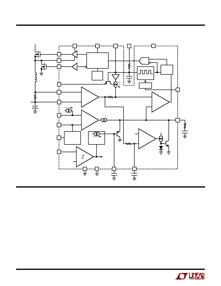
FU
N
CTIO
N
AL BLOCK DIAGRA
U
U
W
OPERATIO
N
U
Basic Control Loop
The LT1339 uses a constant frequency, current mode
synchronous architecture. The timing of the IC is provided
through an internal oscillator circuit, which can be syn-
chronized to an external clock, programmable to operate
at frequencies up to 150kHz. The oscillator creates a
modified sawtooth wave at its timing node (CT) with a slow
charge, rapid discharge characteristic.
During typical positive buck operation, the main switch
MOSFET is enabled at the start of each oscillator cycle. The
main switch stays enabled until the current through the
switched inductor, sensed via the voltage across a series
(Refer to Functional Block Diagram)
sense resistor (R
SENSE
), is sufficient to trip the current
comparator (IC1) and, in turn, reset the RS latch. When the
RS latch resets, the main switch is disabled, and the
synchronous switch MOSFET is enabled. Shoot-through
prevention logic prohibits enabling of the synchronous
switch until the main switch is fully disabled. If the current
comparator threshold is not obtained throughout the
entire oscillator charge period, the RS latch is bypassed
and the main switch is disabled during the oscillator
discharge time. This "minimum off time" assures ad-
equate charging of the bootstrap supply, protects the main
switch, and is typically about 1
µ
s.
+
≠
≠
+
1.25V
SOFT START
8
µ
A
SS
I
AVG
V
C
≠
+
≠
+
EA
1.25V
5V
REFERENCE
V
FB
0.5
µ
A
◊
15
CURRENT
SENSE AMP
IC1
S
R
Q
OSC
SL/ADJ
NONOVERLAPPING
SWITCH LOGIC
UVLO
CIRCUIT
CT
TG
V
BOOST
PHASE
12V
IN
TS
BG
SENSE
+
V
IN
5V
REF
MAIN
SWITCH
SYNC
SWITCH
SENSE
≠
R
SENSE
V
OUT
1339 ∑ BD
CIRCUIT
ENABLE
+
≠
2.5V
PGND
SGND
+
ONE SHOT
50k
AVERAGE
CURRENT
LIMIT
RUN/SHDN
5V
REF
V
REF
SYNC

9
LT1339
OPERATIO
N
U
(Refer to Functional Block Diagram)
The current comparator trip threshold is set on the V
C
pin,
which is the output of a transconductance amplifier, or
error amplifier (EA). The error amplifier integrates the
difference between a feedback voltage (on the V
FB
pin)
and an internal bandgap generated reference voltage of
1.25V, forming a signal that represents required load
current. If the supplied current is insufficient for a given
load, the output will droop, thus reducing the feedback
voltage. The error amplifier forces current out of the V
C
pin, increasing the current comparator threshold. Thus,
the circuit will servo until the provided current is equal to
the required load and the average output voltage is at the
value programmed by the feedback resistors.
Average Current Limit
The output of the sense amplifier is monitored by a single
pole integrator comprised of an external capacitor on the
I
AVG
pin and an internal impedance of approximately
50k
. If this averaged value signal exceeds a level corre-
sponding to 120mV across the external sense resistor, the
current comparator threshold is clamped and cannot
continue to rise in response to the error amplifier. Thus, if
average load current requirements exceed 120mV/R
SENSE
,
the supply will current limit and the output voltage will fall
out of regulation. The average current limit circuit moni-
tors the sense amplifier output without slope compensa-
tion or ripple current contributions, therefore the average
load current limit threshold is unaffected by duty cycle.
Undervoltage Lockout
The LT1339 employs an undervoltage lockout circuit
(UVLO) that monitors the 12V supply rail. This circuit
disables the output drive capability of the LT1339 if
the 12V supply drops below about 9V. Unstable mode
switching is prevented through 350mV of UVLO threshold
hysteresis.
Adaptive Nonoverlapping Output Stage
The FET driver output stage implements adaptive
nonoverlapping control. This circuitry maintains dead
time independent of the type, size or operating conditions
of the switch elements. The control circuit monitors the
output gate drive signals, insuring that the switch gate
(being disabled) is fully discharged before enabling the
other switch driver.
Shutdown
The LT1339 can be put into low current shutdown mode
by pulling the RUN/SHDN pin low, disabling all circuit
functions. The shutdown threshold is a bandgap referred
voltage of 1.25V typical. Use of a precision threshold on
the shutdown circuit enables use of this pin for undervolt-
age protection of the V
IN
supply and/or power supply
sequencing.
Soft Start
The LT1339 incorporates a soft start function that oper-
ates by slowly increasing the internal current limit. This
limit is controlled by clamping the V
C
node to a low voltage
that climbs with time as an external capacitor on the SS pin
is charged with about 8
µ
A. This forces a graceful climb of
output current capability, and thus a graceful increase in
output voltage until steady-state regulation is achieved.
The soft start timing capacitor is clamped to ground
during shutdown and during undervoltage lockout, yield-
ing a graceful output recovery from either condition.
5V Internal Reference
Power for the oscillator timing elements and most other
internal LT1339 circuits is derived from an internal 5V
reference, accessible at the 5V
REF
pin. This supply pin can be
loaded with up to 10mA DC (20mA pulsed) for convenient
biasing of local elements such as control logic, etc.
Slope Compensation
For duty cycles greater than 50%, slope compensation is
required to prevent current mode duty cycle instability in
the regulator control loop. The LT1339 employs internal
slope compensation that is adequate for most applica-
tions. However, if additional slope compensation is
desired, it is available through the SL/ADJ pin. Excessive
slope compensation will cause reduction in maximum
load current capability and therefore is not desirable.
10
LT1339
APPLICATIO
N
S I
N
FOR
M
ATIO
N
W
U
U
U
R
SENSE
Selection for Output Current
R
SENSE
generates a voltage that is proportional to the
inductor current for use by the LT1339 current sense
amplifier. The value of R
SENSE
is based on the required
load current. The average current limit function has a
typical threshold of 120mV/R
SENSE
, or:
R
SENSE
= 120mV/I
LIMIT
Operation with V
SENSE
common mode voltage below 4.5V
may slightly degrade current limit accuracy. See Average
Current Limit Threshold Tolerance vs Common Mode
Voltage curve in the Typical Performance Characteristics
section for more information.
Output Voltage Programming
Output voltage is programmed through a resistor feed-
back network to V
FB
(Pin 9) on the LT1339. This pin is the
inverting input of the error amplifier, which is internally
referenced to 1.25V. The divider is ratioed to provide
1.25V at the V
FB
pin when the output is at its desired value.
The output voltage is thus set following the relation:
V
OUT
= 1.25(1 + R2/R1)
when an external resistor divider is connected to the
output as shown in Figure 1.
the minimum off-time of the PWM controller. This limits
maximum duty cycle (DC
MAX
) to:
DC
MAX
= 1 ≠ (t
DISCH
)(f
O
)
This relation corresponds to the minimum value of the
timing resistor (R
CT
), which can be determined according
to the following relation (R
CT
vs DC
MAX
graph appears in
the Typical Performance Characteristics section):
R
CT(MIN)
[(0.8)(10
≠3
)(1 ≠ DC
MAX
)]
≠1
Values for R
CT
> 15k yield maximum duty cycles above
90%. Given a timing resistor value, the value of the timing
capacitor (C
CT
) can then be determined for desired oper-
ating frequency (f
O
) using the relation:
C
f
R
R
CT
O
CT
CT
( )
-
( )
(
)
+
( )
-
(
)
-
-
1
100 10
1 85
1 75
2 5 10
3 375
9
3
/
/ .
.
.
.
/
A plot of Operating Frequency vs R
CT
and C
CT
is shown in
Figure 2. Typical 100kHz operational values are C
CT
=
1000pF and R
CT
= 16.9k.
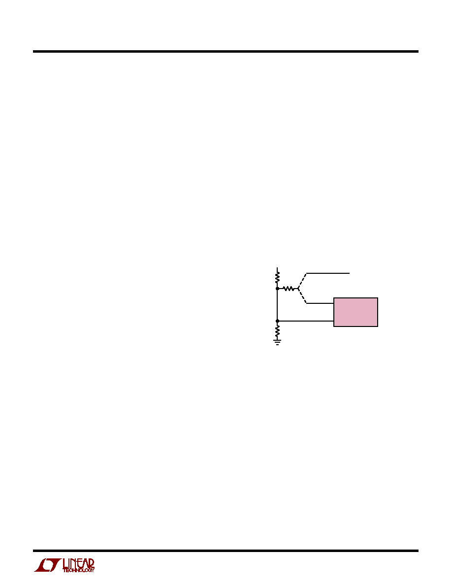
R1
R2
V
OUT
1339 ∑ F01
V
FB
SGND
LT1339
9
8
Figure 1. Programming LT1339 Output Voltage
If high value feedback resistors are used, the input bias
current of the V
FB
pin (1
µ
A maximum) could cause a slight
increase in output voltage. A Thevenin resistance at the
V
FB
pin of <5k is recommended.
Oscillator Components R
CT
and C
CT
The LT1339 oscillator creates a modified sawtooth wave
at its timing node (CT) with a slow charge, rapid discharge
characteristic. The rapid discharge time corresponds to
Figure 2. Oscillator Frequency vs R
CT
, C
CT
Average Current Limit
The average current limit function is implemented using
an external capacitor (C
AVG
) connected from I
AVG
to SGND
that forms a single pole integrator with the 50k
output
TIMING RESISTOR (k
)
0
OSCILLATOR FREQUENCY (kHz)
15
25
LT1339 ∑ F02
5
10
20
160
140
120
100
80
60
40
20
0
30
C
CT
= 3.3nF
C
CT
= 2.2nF
C
CT
= 1.5nF
C
CT
= 1.0nF
11
LT1339
APPLICATIO
N
S I
N
FOR
M
ATIO
N
W
U
U
U
impedance of the I
AVG
pin. The integrator corner fre-
quency is typically set 1 to 2 orders of magnitude below the
oscillator frequency and follows the relation:
f
≠3dB
= (3.2)(10
≠ 6
)/C
AVG
The average current limit function can be disabled by
shorting the I
AVG
pin directly to SGND.
Soft Start Programming
The current control pin (V
C
) limits sensed inductor current
to zero at voltages less than a transistor V
BE
, to full average
current limit at V
C
= V
BE
+ 1.8V. This generates a 1.8V full
regulation range for average load current. An internal
voltage clamp forces the V
C
pin to a V
BE
≠ 100mV above
the SS pin voltage. This 100mV "dead zone" assures 0%
duty cycle operation at the start of the soft start cycle, or
when the soft start pin is pulled to ground. Given the
typical soft start current of 8
µ
A and a soft start timing
capacitor C
SS
, the start-up delay time to full available
average current will be:
t
SS
= (1.5)(10
5
)(C
SS
)
Boost Supply
The V
BOOST
supply is bootstrapped via an external capaci-
tor. This supply provides gate drive to the topside switch
FET. The bootstrap capacitor is charged from 12V
IN
through
a diode when the switch node is pulled low.
The diode reverse breakdown voltage must be greater than
V
IN
+ 12V
IN
. The bootstrap capacitor should be at least 100
times greater than the total input capacitance of the
topside FET. A capacitor in the range of 0.1
µ
F to 1
µ
F is
generally adequate for most applications.
Shutdown Function -- Input Undervoltage Detect and
Threshold Hysteresis
The LT1339 RUN/SHDN pin uses a bandgap generated
reference threshold of about 1.25V. This precision thresh-
old allows use of the RUN/SHDN pin for both logic-level
shutdown applications and analog monitoring applica-
tions such as power supply sequencing.
Because an LT1339 controlled converter is a power trans-
fer device, a voltage that is lower than expected on the
input supply could require currents that exceed the sourc-
ing capabilities of that supply, causing the system to lock
up in an undervoltage state. Input supply start-up protec-
tion can be achieved by enabling the RUN/SHDN pin using
a resistor divider from the input supply to ground. Setting
the divider output to 1.25V when that supply is almost fully
enabled prevents the LT1339 regulator from drawing large
currents until the input supply is able to provide the
required power.
If additional hysteresis is desired for the enable function,
an external feedback resistor can be used from the LT1339
regulator output. If connection to the regulator output is
not desired, the 5V
REF
internal supply pin can be used.
Figure 3 shows a resistor connection on a 48V to 5V
converter that yields a 40V V
IN
start-up threshold for
regulator enable and also provides about 10% input
referred hysteresis.
The shutdown function can be disabled by connecting the
RUN/SHDN pin to the 12V
IN
rail. This pin is internally
clamped to 2.5V through a 20k series input resistance and
will therefore draw about 0.5mA when tied directly to 12V.
This additional current can be minimized by making the
connection through an external resistor (100k is typically
used).
Inductor Selection
The inductor for an LT1339 converter is selected based on
output power, operating frequency and efficiency require-
ments. Generally, the selection of inductor value can be
reduced to desired maximum ripple current in the inductor
(
I). For a buck converter, the minimum inductor value for
a desired maximum operating ripple current can be deter-
mined using the following relation:
10k
300k
V
OUT
5V
1339 ∑ F03
5V
REF
LT1339
2
RUN/SHDN
13
390k
V
IN
48V
OPTION 2
OPTION 1
Figure 3. Input Supply Sequencing Programming
12
LT1339
APPLICATIO
N
S I
N
FOR
M
ATIO
N
W
U
U
U
L
V
V
V
I f
V
MIN
OUT
IN
OUT
O
IN
=
( )
-
(
)
( )( )( )
where f
O
= operating frequency. Given an inductor value
(L), the peak inductor current is the sum of the average
inductor current (I
AVG
)and half the inductor ripple current
(
I), or:
I
I
V
V
V
L f
V
PK
AVG
OUT
IN
OUT
O
IN
=
+
( )
-
(
)
( )( )( )( )
2
The inductor core type is determined by peak current and
efficiency requirements. The inductor core must with-
stand peak current without saturating, and series winding
resistance and core losses should be kept as small as is
practical to maximize conversion efficiency.
The LT1339 peak current limit threshold is 40% greater
than the average current limit threshold. Slope compensa-
tion effects reduce this margin as duty cycle increases.
This margin must be maintained to prevent peak current
limit from corrupting the programmed value for average
current limit. Programming the peak ripple current to less
than 15% of the desired average current limit value will
assure porper operation of the average current limit
feature through 90% duty cycle (see Slope Compensation
section).
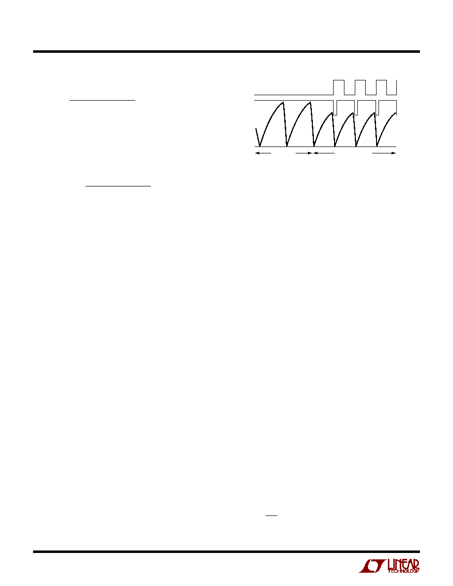
Oscillator Synchronization
The LT1339 oscillator generates a modified sawtooth
waveform at the C
T
pin between low and high thresholds
of about 0.8V (vl) and 2.5V (vh) respectively. The oscillator
can be synchronized by driving a TTL level pulse into the
SYNC pin. This inputs to a one-shot circuit that reduces the
oscillator high threshold to 2V for about 200ns. The SYNC
input signal should have minimum high/low times of
1
µ
s.
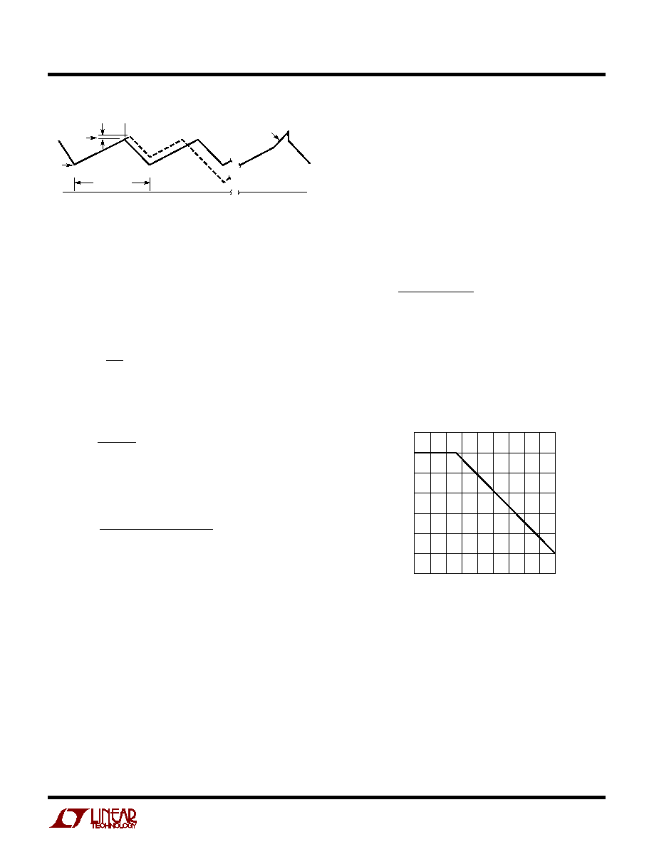
Slope Compensation
Current mode switching regulators that operate with a
duty cycle greater than 50% and have continuous inductor
current can exhibit duty cycle instability. While a regulator
will not be damaged and may even continue to function
acceptably during this type of subharmonic oscillation, an
irritating high-pitched squeal is usually produced.
The criterion for current mode duty cycle instability is met
when the increasing slope of the inductor ripple current is
less than the decreasing slope, which is the case at duty
cycles greater than 50%. This condition is illustrated in
Figure 5a. The inductor ripple current starts at I
1
, at the
beginning of each oscillator switch cycle. Current
increases at a rate S1 until the current reaches the control
trip level I
2
. The controller servo loop then disables the
main switch (and enables the synchronous switch) and
inductor current begins to decrease at a rate S2. If the
current switch point (I
2
) is perturbed slightly and
increased by
I, the cycle time ends such that the mini-
mum current point is increased by a factor of (1 + S2/S1)
to start the next cycle. On each successive cycle, this error
is multiplied by a factor of S2/S1. Therefore, if S2/S1 is
1, the system is unstable.
Subharmonic oscillations can be eliminated by augment-
ing the increasing ripple current slope (S1) in the control
loop. This is accomplished by adding an artificial ramp on
the inductor current waveform internal to the IC (with a
slope S
X
) as shown in Figure 5b. If the sum of the slopes
S1 + S
X
is greater than S2, the condition for subharmonic
oscillation no longer exists.
For a buck converter, the required additional current
waveform slope, or "Slope Compensation," follows the
relation:
S
V
L
DC
X
IN
-
(
)
2
1
0.8V
1339 F04
2V
2.5V
(vl)
SYNC
V
CT
(vh)
FREE RUN
SYNCHRONIZED
Figure 4. Free Run and Synchronized Oscillator
Waveforms (at C
T
Pin)
13
LT1339
APPLICATIO
N
S I
N
FOR
M
ATIO
N
W
U
U
U
For duty cycles less than 50% (DC < 0.5), S
X
is negative
and is not required. For duty cycles greater than 50%, S
X
takes on values dependent on S1 and duty cycle. This leads
to a minimum inductance requirement for a given V
IN
and
duty cycle of:
L
V
S
DC
MIN
IN
X
=
-
(
)
2
1
The LT1339 contains an internal S
X
slope compensation
ramp that has an equivalent current referred value of:
0.084
f
R
O
SENSE
Amp/s
where f
O
is oscillator frequency. This yields a minimum
inductance requirement of:
L
V
R
DC
f
MIN
IN
SENSE
O
( )(
)
-
(
)
( )( )
2
1
0 084
.
A down side of slope compensation is that, since the IC
servo loop senses an increase in perceived inductor cur-
rent, the internal current limit functions are affected such
that the maximum current capability of a regulator is
reduced by the same amount as the effective current
referred slope compensation. The LT1339, however, uses
a current limit scheme that is independent of slope com-
pensation effects (average current limit). This provides
operation at any duty cycle with no reduction in current
sourcing capability, provided ripple current peak ampli-
tude is less than 15% of the current limit value. For
example, if the supply is set up to current limit at 10A, as
long as the peak inductor current is less than 11.5A, duty
cycles up to 90% can be achieved without compromising
the average current limit value.
If an inductor smaller than the minimum required for
internal slope compensation (calculated above as L
MIN
) is
desired, additional slope compensation is required. The
LT1339 provides this capability through the SL/ADJ pin.
This feature is implemented by referencing this pin via a
resistor divider from the 5V
REF
pin to ground. The addi-
tional slope compensation will be affected at the point in
the oscillator waveform (at pin CT) corresponding to the
voltage set by the resistor divider. Additional slope com-
pensation can be calculated using the relation:
S
f
R
R
XADD
O
EQ
SENSE
=
(
)( )
( )(
)
2500
Amp/s
where R
EQ
is the effective resistance of the resistor divider.
Actual compensation will be somewhat greater due to
internal curvature correction circuitry that imposes an
exponential increase in the slope compensation wave-
form, further increasing the effective compensation slope
up to 20% for a given setting.
OSCILLATOR
PERIOD
TIME
0
0
a
b
I
T1
I
2
I
1
S1
S1
S2
S2
S1 + S
X
1339 ∑ F05
Figure 5. Inductor Current at DC > 50% and
Slope Compensation Adjusted Signal
DUTY CYCLE (DC)
0
PEAK
/
AVG
0.4
1.45
1.40
1.35
1.30
1.25
1.20
1.15
1.10
LT1339 ∑ F06
0.2
0.6
0.1
0.5
0.3
0.7 0.8 0.9
Figure 6. Maximum Ripple Current (Normalized)
vs Duty Cycle for Average Current Limit
Design Example:
V
IN
= 20V
V
OUT
= 15V (DC = 0.75)
R
SENSE
= 0.01
f
O
= 100kHz
L = 5
µ
H
The minimum inductor usable with no additional slope
compensation is:

14
LT1339
APPLICATIO
N
S I
N
FOR
M
ATIO
N
W
U
U
U
R
SL1
= 45k and R
SL2
= 30k sets the desired reference
voltage and has a R
EQ
of 18k, which meets both design
requirements. Figure 7b shows the slope compensation
effective waveforms both with and without the SL/ADJ
external resistors.
Power MOSFET and Catch Diode Selection
External N-channel MOSFET switches are used with the
LT1339. The positive gate-source drive voltage of the
LT1339 for both switches is roughly equivalent to the
12V
IN
supply voltage, so standard threshold MOSFETs
can be used.
Selection criteria for the power MOSFETs include the "ON"
resistance (R
DS(ON)
), reverse transfer capacitance (C
RSS
),
maximum drain-source voltage (V
DSS
) and maximum
output current.
The power FETs selected must have a maximum operating
V
DSS
exceeding the maximum V
IN
. V
GS
voltage maximum
must exceed the 12V
IN
supply voltage.
Once voltage requirements have been determined, R
DS(ON)
can be selected based on allowable power dissipation and
required output current.
In an LT1339 buck converter, the average inductor current
is equal to the DC load current. The average currents
through the main and synchronous switches are:
I
MAIN
= (I
LOAD
)(DC)
I
SYNC
= (I
LOAD
)(1 ≠ DC)
The R
DS(ON)
required for a given conduction loss can be
calculated using the relation:
P
LOSS
= (I
SWITCH
)
2
(R
DS(ON)
)
In high voltage applications (V
IN
> 20V), the topside switch
is required to slew very large voltages. As V
IN
increases,
transition losses increase through a square relation, until
it becomes the dominant power loss term in the main
switch. This transition loss takes the form:
P
TR
(k)(V
IN
)
2
(I
MAX
)(C
RSS
)(f
O
)
where k is a constant inversely related to the gate drive
current, approximated by k = 2 in LT1339 applications.
L
V
H
MIN
( )
( )
-
( )
( )(
)
=
µ
20
0 01
1 5 1
0 084 100000
11 9
.
.
.
.
Since L = 5
µ
H is less than L
MIN
, additional slope compen-
sation is necessary. The total slope compensation
required is:
S
V
H
X
µ
-
( )
=
( )
20
5
1 5 1
2 10
6
.
Amp/s
Subtracting the internally generated slope compensation
and solving for the required effective resistance at SL/ADJ
yields:
R
f
R
f
k
EQ
O
SENSE
O
( )( )
( )
(
)
-
( )( )
=
2500
2 10
0 084
21 5
6
.
.
Setting the resistor divider reference voltage at 2V assures
that the additional compensation waveform will be
enabled at 75% duty cycle. As shown in Figure 7a, using
R
SL2
30k
R
SL1
45k
1339 ∑ F07a
5V
REF
LT1339
2
SL/ADJ
4
Figure 7a. External Slope Compensation Resistors
Figure 7b. Slope Compensation Waveforms
(0.084 + 0.139)(f
O
)
R
SENSE
(0.084)(f
O
)
R
SENSE
2.5V
2V
0.8V
DC = 0.75
1339 ∑ F07b

15
LT1339
APPLICATIO
N
S I
N
FOR
M
ATIO
N
W
U
U
U
V
OUT
I
L
{ESR + [(4)(f
O
)
∑
C
OUT
]
≠1
}
where f
O
= operating frequency.
Efficiency Considerations and Heat Dissipation
High output power applications have inherent concerns
regarding power dissipation in converter components.
Although high efficiencies are achieved using the LT1339,
the power dissipated in the converter climbs to relatively
high values when the load draws large amounts of power.
Even at 90% efficiency, an application that provides 500W
to the load has conversion loss of 55W.
I
2
R dissipation through the switches, sense resistor and
inductor series resistance create substantial losses under
high currents. Generally, the dominant I
2
R loss is evident
in the FET switches. Loss in each switch is proportional to
the conduction time of that switch. For example, in a 48V
to 5V converter the synchronous FET conducts load cur-
rent for almost 90% of the cycle time and thus, requires
greater consideration for dissipating I
2
R power.
Gate charge/discharge current creates additional current
drain on the 12V supply. If powered from a high voltage
input through a linear regulator, the losses in that regula-
tor device can become significant. A supply solution
bootstrapped from the output would draw current from a
lower voltage source and reduce this loss component.
Transition losses are significant in the topside switch FET
when high V
IN
voltages are used. Transition losses can be
estimated as:
P
TLOSS
2(V
IN
)
2
(I
MAX
)(C
RSS
)(f
O
)
Since the conduction time in the main switch of a 48V to
5V converter is small, the I
2
R loss in the main switch FET
is also small. However, since the FET gate must switch up
past the 48V input voltage, transition loss can become a
significant factor. In such a case, it is often prudent to take
the increased I
2
R loss of a smaller FET in order to reduce
C
RSS
and thus, the associated transition losses.
Gate Drive Buffers
The LT1339 is designed to drive relatively large capacitive
loads. However, in certain applications, efficiency im-
provements can be realized by adding an external buffer
stage to drive the gates of the FET switches. When the
The maximum power loss terms for the switches are thus:
P
MAIN
= (DC)(I
MAX
)
2
(1 +
)(R
DS(ON)
) +
2(V
IN
)
2
(I
MAX
)(C
RSS
)(f
O
)
P
SYNC
= (1 ≠ DC)(I
MAX
)
2
(1 +
)(R
DS(ON)
)
The (1 +
) term in the above relations is the temperature
dependency of R
DS(ON)
, typically given in the form of a
normalized R
DS(ON)
vs Temperature curve in a MOSFET
data sheet.
In some applications, parasitic FET capacitances couple
the negative going switch node transient onto the bottom
gate drive pin of the LT1339, causing a negative voltage in
excess of the Absolute Maximum Rating to be imposed on
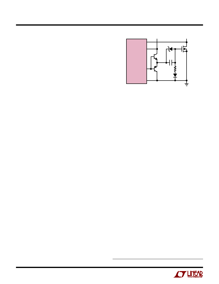
that pin. Connection of a catch Schottky (rated to about 1A
is typically sufficient) from this pin to ground will eliminate
this effect.
C
IN
and C
OUT
Supply Decoupling Capacitor Selection
The large currents typical of LT1339 applications require
special consideration for the converter input and output
supply decoupling capacitors. Under normal steady state
operation, the source current of the main switch MOSFET
is a square wave of duty cycle V
OUT
/V
IN
. Most of this
current is provided by the input bypass capacitor. To
prevent large input voltage transients and avoid bypass
capacitor heating, a low ESR input capacitor sized for the
maximum RMS current must be used. This maximum
capacitor RMS current follows the relation:
I
I
V
V
V
V
RMS
MAX
OUT
IN
OUT
IN
(
)
(
)
(
)
≠
/
1 2
which peaks at a 50% duty cycle, when I
RMS
= I
MAX
/2.
Capacitor ripple current ratings are often based on only
2000 hours (three months) lifetime; it is advisable to
derate either the ESR or temperature rating of the capaci-
tor for increased MTBF of the regulator.
The output capacitor in a buck converter generally has
much less ripple current than the input capacitor. Peak-to-
peak ripple current is equal to that in the inductor (
I
L
),
typically a fraction of the load current. C
OUT
is selected to
reduce output voltage ripple to a desirable value given an
expected output ripple current. Output ripple (
V
OUT
) is
approximated by:
16
LT1339
APPLICATIO
N
S I
N
FOR
M
ATIO
N
W
U
U
U
switch gates load the driver outputs such that rise/fall
times exceed about 100ns, buffers can sometimes result
in efficiency gains. Buffers also reduce the effect of back
injection into the bottom side driver output due to coupling
of switch node transitions through the switch FET C
MILLER
.
Paying the Physicists
In high power synchronous buck configurations, certain
physical characteristics of the external MOSFET switches
can impact conversion efficiency. As the input voltage
approaches about 30V, the bottom MOSFETs will begin to
exhibit "phantom turn-on." This phenomenon is caused
by coupling of the instantaneous voltage step on the
bottom side switch drain through C
MILLER
to the device
gate, yielding internal localized gate-source voltages above
the turn-on threshold of the FET. This generates a shoot-
through blip that ultimately eats away at efficiency num-
bers. In Figure 8 a negative prebias circuit is added to the
bottom side gate. The addition of this
3V of negative
offset to the bottom gate drive provides additional off-
state voltage range to prevent phantom turn-on.
This type of prebias circuit is used in the 48V to 5V, 50A
converter pictured in the Typical Applications section.
As currents increase beyond the 10A to 15A range, the
bottom side FET body diode experiences hard turn-on
during switch dead time due to local current loop induc-
tance preventing the timely transfer of charge to the
Schottky catch diode. The charge current required to
commutate this body diode creates a high dV/dt Schottky
avalanche when the diode charge is finally exhausted (due
to an effective inductor current discontinuity at the
moment the body diode no longer requires charge). This
generates an increased turn-on power burst in the topside
switch, causing additional conversion efficiency loss. This
effect of this parasitic inductance can be reduced by using
FETKEY
TM
MOSFETs, which have parallel catch Schottky
diodes internal to their packages.
FETKEY MOSFETs are
FETKEY is a trademark of International Rectifier Corporation.
TS
12V
IN
BG
PGND
LT1339
ZTX649
ZTX749
D1N914
1339 F08
10k
1
µ
F
3.3V
Figure 8. Bottom Side Driver Negative Prebias Circuit
not available for high voltages, so as input voltage contin-
ues to increase, they can no longer be used. Because this
necessitates the use of discrete FETs and Schottkys,
interdigitation of a number of smaller devices is required
to minimize parasitic inductances. This technique is also
used in the 48V to 5V, 50A converter shown in the Typical
Applications section.
Optimizing Transient Response--Compensation
Component Values
The dominant compensation point for an LT1339 con-
verter is the V
C
pin (Pin 7), or error amplifier output. This
pin is connected to a series RC network, R
VC
and C
VC
. The
infinite permutations of input/output filtering, capacitor
ESR, input voltage, load current, etc. make for an empirical
method of optimizing loop response for a specific set of
conditions.
Loop response can be observed by injecting a step change
in load current. This can be achieved by using a switchable
load. With the load switching, the transient response of the
output voltage can be observed with an oscilloscope.
Iterating through RC combinations will yield optimized
response. Refer to LTC Application Note 19 in
1990 Linear
Applications Handbook, Volume 1 for more information.
17
LT1339
TYPICAL APPLICATIO
N
S
U
6
7
10
20
19
18
11
12
16
14
13
9
17
U1
LT1339
12V
15
8
C14
3300pF
C12
100pF
R9
12k
R10
10k
1%
R8
301k
1%
R6, 100
R7
100
D5
BAT54
+
+
+
+
+
1339 TA05
T1
1
3:2
C1: SANYO 63MV680GX
C2: WIMA SMD4036/1.5/63/20/TR
C6: KEMET T510X477M006AS (X8)
L1: GOWANDA 50-318
T1: GOWANDA 50-319
L1
1.5
µ
H
R5
2.49k
1%
SS
V
C
V
REF
V
BOOST
TG
TS
SENSE
+
SENSE
≠
BG
PHASE
RUN/SHDN
V
FB
SGND
12V
IN
PGND
C15
0.1
µ
F
C10
0.1
µ
F
C9
1800pF
5%
NPO
C11
0.1
µ
F
D2
MURS120
D4
MBR0530T1
SYNC
1
2
4
3
5
5V
REF
SL/ADJ
CT
I
AVG
8
7
6
5
V
CC1
OUT1
V
CC2
OUT2
IN1
GND1
IN2
GND2
1
2
3
4
U2, LTC1693-2
8
7
6
5
V
CC1
OUT1
V
CC2
OUT2
IN1
GND1
IN2
GND2
1
2
3
4
U3, LTC1693-2
+
C7
1
µ
F
+
C13
1
µ
F
+
C5
1
µ
F
+
C1
680
µ
F
63V
Q1
MTD20N06HD
D3
MURS120
Q3
MTD20N06HD
4
3
21
D1
MURS120
+
C8
1
µ
F
R1
0.04
8
7
6
5
4
Q4
Si4420
X2
Q2
Si4420
X2
V
OUT
1,8V
20A
3
21
8
7
6
5
+
C3
4700pF
25V
R2
5.1
+
C6
470
µ
F
6.3V
X8
+
C4
0.1
µ
F
R3
549
1%
R4
1.24k
1%
V
IN
48V
+
C2
1.5
µ
F
63V
+
48V to 1.8V 2-Transistor Synchronous Forward Converter
18
LT1339
TYPICAL APPLICATIO
N
S
U
W2
T2
W1
W3
6
5
7
2
V
CC2
OUT2
OUT1
GND1
V
CC1
IN2
IN1
GND2
8
3
1
4
LTC1693-1
6
5
7
2
V
CC2
OUT2
OUT1
GND1
GND2
IN2
V
CC1
IN1
4
3
8
1
LTC1693-1
V
+
COMP
RTOP
GND-F
GND-S
RMID
65
7
32
4
T2
T1
W4
T2
4.7k
470
470
BAT54
BAT54
W5
W1
W4
SUD30N04-10
SUD30N04-10
IRF1310NS
1nF
SEC HV
10
10
4.8
µ
H
PANASONIC ETQP AF4R8H
1nF
C3
330
µ
F
6.3V
C4
330
µ
F
6.3V
C5
330
µ
F
6.3V
10
4.7nF
4.7nF
47
0.1
µ
F
T2
W3
4.7k
+
+
+
≠V
OUT
+V
OUT
≠V
OUT
+V
OUT
OUTPUT
5V/10A
C3, C4, C5:
SANYO OS-CON
1
µ
F
FZT600
4.7
µ
F
25V
0.47
µ
F
50V
2k
3.1V
MMFT3904
10
BAS21
SEC HV
LT1431CS8
REF
COLL
18
1k
470
100k
3.01k
1%
4.42k
1%
9.31k
1%
0.01
µ
F
+V
OUT
0.22
µ
F
1k
≠V
OUT
SHORT JP1
FOR 5V
OUT
V
BOOST
TG
TS
SENSE
+
SENSE
≠
12V
IN
RUN/SHDN
PHASE
BG
V
FB
SYNC
5V
REF
CT
SL/ADJ
I
AVG
V
REF
SGND
PGND
SS
V
C
LT1339
+
100k
+V
IN
13k
100k
2.4k
4.53k
0.1
µ
F
1
µ
F
2.2nF
2.2nF
0.1
µ
F
4.7nF
68
µ
F
20V
AVX
TSPE
3.9k
17
13
14
1
20
19
18
11
12
2
3
4
5
10
8
1
5
6
7
16
9
MMBD914LT1
3.3
1
µ
F
CNY17-3
P
P
36k
BAS21
BAS21
BAS21
P
JP2
JP3
5V
OUT
SHORT JP3, OPEN JP2
3.3V
OUT
, SHORT JP2, OPEN JP3
COILCRAFT
DO1608-105
T1
10k
10
2.2
µ
F
0.025
1/2W
470
10
FMMT718
FMMT718
P
IRF1310NS
MURS120
MURS120
12V
2.2
µ
F
MMBD914LT1
470
BAT54
W2
C1
1.2
µ
F
100V
CER
C2
1.2
µ
F
100V
CER
+V
IN
P
≠V
IN
+V
IN
+V
IN
W3, 10T 32AWG,
W4, 10T 32AWG
W5, 10T 2 x 26AWG
W4, 7T 6 x 26AWG
W1, 18T BIFILAR 31AWG
W3, 6T BIFILAR 31AWG
W1, 10T 2 x 26AWG
W1, 10T 32AWG,
W2, 15T 32AWG
2MIL
POLY
FILM
2MIL
POLY
FILM
OUTPUT CURRENT
0123456789
1
0
EFFICIENCY
95
90
85
36V
IN
48V
IN
72V
IN
T1 PHILIPS EFD20-3F3 CORE
L
P
= 720
µ
H (AI = 1800)
T2 ER11/5 CORE
AI = 960
µ
H
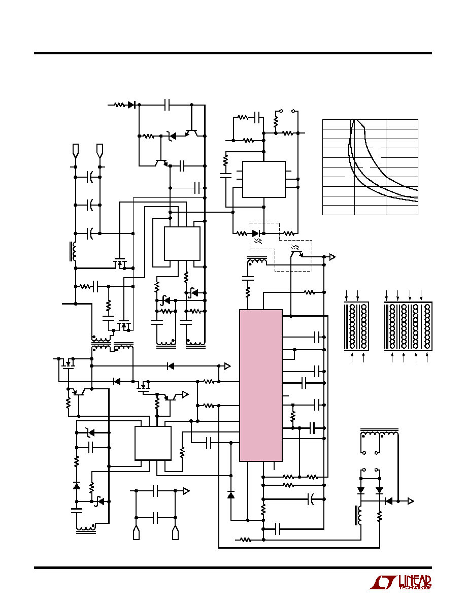
1339 TA06
INPUT
36V TO
75V
48V to 5V Isolated Synchronous Forward DC/DC Converter
19
LT1339
Information furnished by Linear Technology Corporation is believed to be accurate and reliable.
However, no responsibility is assumed for its use. Linear Technology Corporation makes no represen-
tation that the interconnection of its circuits as described herein will not infringe on existing patent rights.
SW Package
20-Lead Plastic Small Outline (Wide 0.300)
(LTC DWG # 05-08-1620)
S20 (WIDE) 0396
NOTE 1
0.496 ≠ 0.512*
(12.598 ≠ 13.005)
20
19
18
17
16
15
14
13
1
2
3
4
5
6
7
8
0.394 ≠ 0.419
(10.007 ≠ 10.643)
9
10
11
12
0.037 ≠ 0.045
(0.940 ≠ 1.143)
0.004 ≠ 0.012
(0.102 ≠ 0.305)
0.093 ≠ 0.104
(2.362 ≠ 2.642)
0.050
(1.270)
TYP
0.014 ≠ 0.019
(0.356 ≠ 0.482)
TYP
0
∞
≠ 8
∞
TYP
NOTE 1
0.009 ≠ 0.013
(0.229 ≠ 0.330)
0.016 ≠ 0.050
(0.406 ≠ 1.270)
0.291 ≠ 0.299**
(7.391 ≠ 7.595)
◊
45
∞
0.010 ≠ 0.029
(0.254 ≠ 0.737)
NOTE:
1. PIN 1 IDENT, NOTCH ON TOP AND CAVITIES ON THE BOTTOM OF PACKAGES ARE THE MANUFACTURING OPTIONS.
THE PART MAY BE SUPPLIED WITH OR WITHOUT ANY OF THE OPTIONS
DIMENSION DOES NOT INCLUDE MOLD FLASH. MOLD FLASH SHALL NOT EXCEED 0.006" (0.152mm) PER SIDE
DIMENSION DOES NOT INCLUDE INTERLEAD FLASH. INTERLEAD FLASH SHALL NOT EXCEED 0.010" (0.254mm) PER SIDE
*
**
PACKAGE DESCRIPTIO
N
U
Dimensions in inches (millimeters) unless otherwise noted.
N Package
20-Lead PDIP (Narrow 0.300)
(LTC DWG # 05-08-1510)
N20 1197
0.020
(0.508)
MIN
0.125
(3.175)
MIN
0.130
±
0.005
(3.302
±
0.127)
0.065
(1.651)
TYP
0.045 ≠ 0.065
(1.143 ≠ 1.651)
0.018
±
0.003
(0.457
±
0.076)
0.005
(0.127)
MIN
0.100
±
0.010
(2.540
±
0.254)
0.009 ≠ 0.015
(0.229 ≠ 0.381)
0.300 ≠ 0.325
(7.620 ≠ 8.255)
0.325
+0.035
≠0.015
+0.889
≠0.381
8.255
(
)
0.255
±
0.015*
(6.477
±
0.381)
1.040*
(26.416)
MAX
1
2
3
4
5
6
7
8
9
10
19
11
12
13
14
16
15
17
18
20
*THESE DIMENSIONS DO NOT INCLUDE MOLD FLASH OR PROTRUSIONS.
MOLD FLASH OR PROTRUSIONS SHALL NOT EXCEED 0.010 INCH (0.254mm)
TYPICAL APPLICATIO
N
S
U
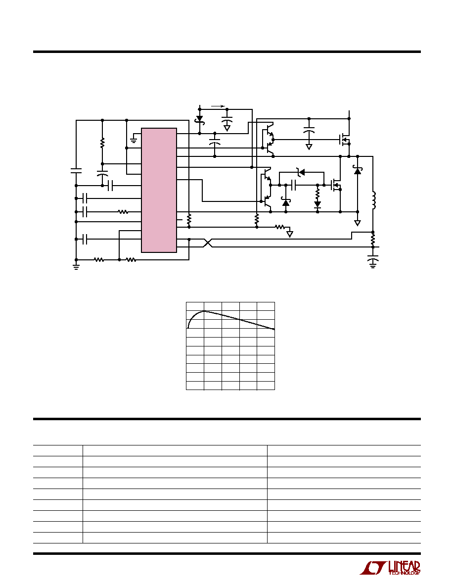
5V to 28V DC/DC Synchronous Boost Converter Limits Input Current at 60A (DC)
V
BOOST
TG
TS
12V
IN
BG
PGND
PHASE
RUN/SHDN
SENSE
≠
SENSE
+
12V
C
12VIN
47
µ
F
IRF3205
◊
2
IRF3205
◊
4
L1
40
µ
H
V
IN
5V AT 60A
R
FB2
, 1.2k
R
FB1
, 27k
SYNC
5V
REF
CT
SL/ADJ
I
AVG
SS
V
C
SGND
V
FB
V
REF
LT1339
+
CBST
1
µ
F
+
C
IN
2200
µ
F
6.3V
◊
4
+
C
12L
1
µ
F
+
R
R1
100k
R
CT
10k
C
CT
2200pF
C
AVG
2200pF
C
SS
, 10
µ
F
C
VC
, 1500pF
R
VC
, 7.5k
C
REF
, 0.1
µ
F
1339 TA04
L1 = 12T 4X12 ON 77439-A7
C
5VREF
1
µ
F
DBST
MBR0530
Q1
FMMT619
Q2
FMMT720
Q3
FMMT619
Q4
FMMT720
D2
MBR0520
D1
IR30BQ060
◊
8
R
SS2
, 100
R
SS1
100
R
S
0.002
C
OUT
2200
µ
F
35V
◊
6
+
V
OUT
28V
+
+
20
LT1339
©
LINEAR TECHNOLOGY CORPORATION 1997
1339fa LT/TP 0299 2K REV A ∑ PRINTED IN THE USA
TYPICAL APPLICATIO
N
U
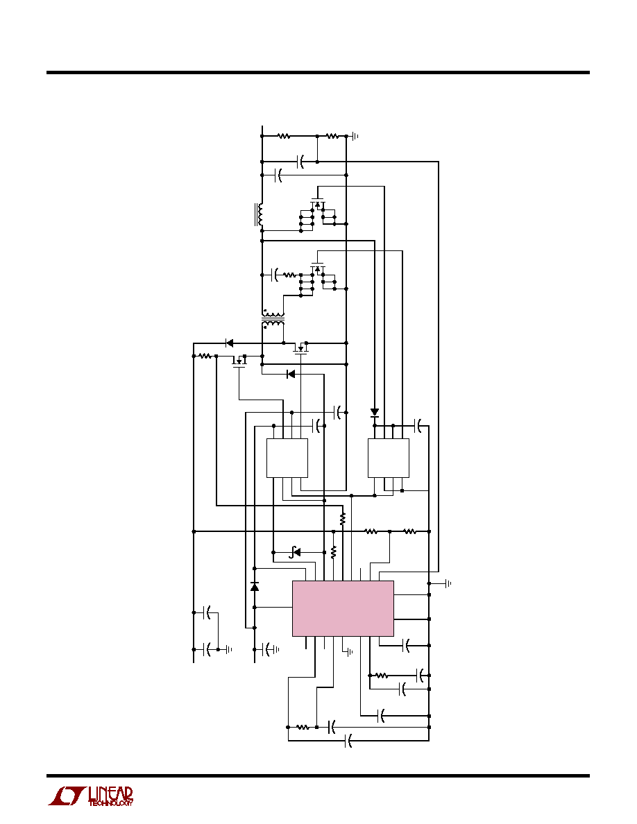
48V to 5V 50A DC/DC Converter with Input Supply Start-Up Protection
RELATED PARTS
PART NUMBER
DESCRIPTION
COMMENTS
LT1158
Half-Bridge N-Channel MOSFET Driver
Current Limit Protection, 100% of Duty Cycle
LT1160
Half-Bridge N-Channel MOSFET Driver
Up to 60V Input Supply, No Shoot-Through
LT1162
Dual Half-Bridge N-Channel MOSFET Driver
V
IN
to 60V, Good for Full-Bridge Applications
LT1336
Half-Bridge N-Channel MOSFET Driver
Smooth Operation at High Duty Cycle (95% to 100%)
LTC
Æ
1530
High Power Step-Down Switching Regulator Controller
Excellent for 5V to 3.xV Up to 50A
LTC1435A
High Efficiency, Low Noise Current Mode Step-Down DC/DC Converter
Drives Synchronous N-Channel MOSFETs
LTC1438
Dual High Efficiency, Low Noise Synchronous Step-Down Controller
Tight 1% Reference
LT1680
High Power DC/DC Current Mode Step-Up Controller
High Side Current Sense, Up to 60V Input
SYNC
5V
REF
CT
SL/ADJ
I
AVG
SS
V
C
SGND
V
FB
V
REF
V
BOOST
TG
TS
12V
IN
BG
PGND
PHASE
RUN/SHDN
SENSE
≠
SENSE
+
12V
C
12VIN
47
µ
F
IRFZ44
◊
2
IRFZ44
◊
4
L1
40
µ
H
V
OUT
5V AT 50A
R
FB2
1k
R
FB1
3k
LT1339
+
CBST
1
µ
F
+
C
OUT
2200
µ
F
6.3V,
◊
4
+
R
R1
22k
R
R3
51k
R
CT
10k
+
C
CT
2200pF
C
AVG
, 2200pF
C
SS
,
10
µ
F
C
VC
, 2200pF
R
VC
, 4.7k
C
REF
0.1
µ
F
1339 TA01
D1 = IR30BQ060
◊
8
Q1, Q3 = FMMT619; Q2, Q4 = FMMT720
L1 = Kool M
µ
Æ
, 12T 4X12 ON 77439-A7
Kool M
µ
IS A REGISTERED TRADEMARK OF MAGNETICS, INC.
C
5VREF
1
µ
F
DBST
IN5819
Q1
Q2
Q3
Q4
D2
MBR0520
D4
IN914
D1
R
S
0.002
C
IN
1500
µ
F
63V,
◊
6
+
V
IN
48V
R
R2
1.2k
C
BG
,
1
µ
F
D3
MMSZ4684
R
BG
10k
50mA
48V to 5V Efficiency
OUTPUT CURRENT (AMPS)
0
EFFICIENCY (%)
100
95
90
85
80
75
70
65
60
55
50
40
LT1339 ∑ TA02
10
20
30
50
Linear Technology Corporation
1630 McCarthy Blvd., Milpitas, CA 95035-7417
(408) 432-1900
q
FAX: (408) 434-0507
q
www.linear-tech.com