 | ÐлекÑÑоннÑй компоненÑ: LT1342 | СкаÑаÑÑ:  PDF PDF  ZIP ZIP |
Äîêóìåíòàöèÿ è îïèñàíèÿ www.docs.chipfind.ru
1
LT1342
5V RS232 Transceiver with
3V Logic Interface
S
FEATURE
The LT
®
1342 is an advanced low power three-driver, five-
receiver RS232 transceiver. The LT1342 operates from a
5V supply and a 3V logic supply. Receiver outputs can
interface directly to 3V logic circuits. Included on the chip
is a shutdown pin for reducing supply current to near zero.
All receivers and drivers assume high impedance states
during shutdown.
The driver disable function provides additional control of
operating mode. When driver disable is high the charge
pump and drivers turn off. Receivers continue to operate
during driver disable.
New ESD structures on the chip allow the LT1342 to
survive multiple
±
10kV strikes, eliminating the need for
costly TransZorbs
®
on the RS232 line pins.
The LT1342 is fully compliant with all EIA RS232 specifi-
cations and operates in excess of 120kbaud even driving
heavy capacitive loads.
s
ESD Protection Over
±
10kV
s
3V Logic Interface
s
Uses Small Capacitors: 0.1
µ
F, 0.2
µ
F
s
1
µ
A Supply Current in Shutdown
s
Low Power Driver Disable Operating Mode
s
Pin Compatible with LT1137A
s
120kBaud Operation for R
L
= 3k, C
L
= 2500pF
s
250kBaud Operation for R
L
= 3k, C
L
= 1000pF
s
CMOS Comparable Low Power: 60mW
s
Operates from a 5V Supply and 3V Logic Supply
s
Easy PC Layout: Flowthrough Architecture
s
Rugged Bipolar Design
s
Outputs Assume a High Impedance State When
Off or Powered Down
s
Absolutely No Latchup
D
U
ESCRIPTIO
, LTC and LT are registered trademarks of Linear Technology Corporation.
TransZorb is a registered trademark of General Instruments, GSI.
s
Notebook Computers
s
Palmtop Computers
U
S
A
O
PPLICATI
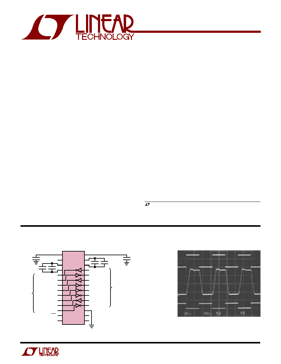
Output Waveforms
R
LT1342 · TA02
U
A
O
PPLICATI
TYPICAL
RECEIVER
OUTPUT
V
L
= 3V
C
L
= 50pF
DRIVER
OUTPUT
R
L
= 3k
C
L
= 2500pF
INPUT
1
2
3
4
5
6
7
8
9
10
11
12
13
14
28
27
26
25
24
23
22
21
20
19
18
17
16
15
5V V
CC
DRIVER 1 OUT
RX1 IN
DRIVER 2 OUT
RX2 IN
RX3 IN
RX4 IN
DRIVER 3 OUT
RX5 IN
ON/OFF
3V V
L
DRIVER 1 IN
RX1 OUT
DRIVER 2 IN
RX2 OUT
RX3 OUT
RX4 OUT
DRIVER 3 IN
RX5 OUT
V
+
0.1
µ
F
2
×
0.1
µ
F
2
×
0.1
µ
F
0.1
µ
F
GND
DRIVER DISABLE
TO LINE
TO 3V LOGIC
V
LT1342 · TA01
LT1342
NC
2
LT1342
A
U
G
W
A
W
U
W
A
R
BSOLUTE
XI
TI
S
W
U
U
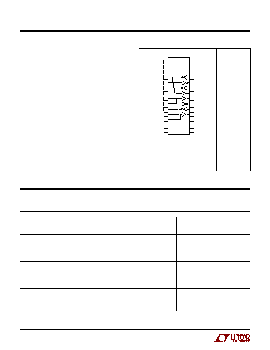
PACKAGE/ORDER I FOR ATIO
ORDER PART
NUMBER
1
2
3
4
5
6
7
8
9
10
11
12
13
14
V
+
5V V
CC
C1
+
C1
DRIVER 1 OUT
RX1 IN
DRIVER 2 OUT
RX2 IN
RX3 IN
RX4 IN
DRIVER 3 OUT
ON/OFF
3V V
L
28
27
26
25
24
23
22
21
20
19
18
17
16
15
V
C2
C2
+
DRIVER 1 IN
RX1 OUT
DRIVER 2 IN
RX2 OUT
RX3 OUT
RX4 OUT
DRIVER 3 IN
GND
NC
NW PACKAGE
28-LEAD WIDE PDIP
TOP VIEW
SW PACKAGE
28-LEAD WIDE PLASTIC SO
G PACKAGE
28-LEAD PLASTIC SSOP
RX5 IN
RX5 OUT
DRIVER
DISABLE
Consult factory for Industrial and Military grade parts.
LT1342CG
LT1342CNW
LT1342CSW
PARAMETER
CONDITIONS
MIN
TYP
MAX
UNITS
Power Supply Generator
V
+
Output
8.6
V
V
Output
7
V
Supply Current (V
CC
)
(Note 3)
12
17
mA
Logic Supply Current (V
L
)
(Note 4)
0.1
1
mA
Supply Current When OFF (V
CC
)
Shutdown (Note 5)
q
1
10
µ
A
Driver Disable
3
mA
Logic Supply Current (V
L
) When OFF
Shutdown (Note 5)
q
1
10
µ
A
Driver Disable
0.1
1
mA
Supply Rise Time
C1 = C2 = 0.2
µ
F,
0.2
ms
Shutdown to Turn-On
C
+
= C
= 0.1
µ
F
ON/OFF Pin Thresholds
Input Low Level (Device Shutdown)
q
1.4
0.8
V
Input High Level (Device Enabled)
q
2.4
1.4
V
ON/OFF Pin Current
0V
V
ON/OFF
5V
q
15
80
µ
A
DRIVER DISABLE Pin Thresholds
Input Low Level (Drivers Enabled)
q
1.4
0.8
V
Input High Level (Drivers Disabled)
q
2.4
1.4
V
DRIVER DISABLE Pin Current
0V
V
DRIVER DISABLE
5V
q
10
500
µ
A
Oscillator Frequency
130
kHz
ELECTRICAL C
C
HARA TERISTICS
(Note 2)
T
JMAX
= 125
°
C,
JA
= 96
°
C/ W (G)
T
JMAX
= 125
°
C,
JA
= 56
°
C/ W (NW)
T
JMAX
= 125
°
C,
JA
= 85
°
C/ W (SW)
(Note 1)
Supply Voltage (V
CC
) ................................................ 6V
Supply Voltage (V
L
) .................................................. 6V
V
+
........................................................................ 13.2V
V
...................................................................... 13.2V
Input Voltage
Driver ........................................................... V
to V
+
Receiver ................................................ 30V to 30V
Output Voltage
Driver .................................................... 30V to 30V
Receiver .................................... 0.3V to V
CC
+ 0.3V
Short-Circuit Duration
V
+
................................................................... 30 sec
V
................................................................... 30 sec
Driver Output .............................................. Indefinite
Receiver Output .......................................... Indefinite
Operating Temperature Range .................... 0
°
C to 70
°
C
Storage Temperature Range ................ 65
°
C to 150
°
C
Lead Temperature (Soldering, 10 sec)................. 300
°
C
3
LT1342
ELECTRICAL C
C
HARA TERISTICS
(Note 2)
The
q
denotes specifications which apply over the full operating
temperature range (0
°
C
T
A
70
°
C for commercial grade).
Note 1: Absolute Maximum Ratings are those values beyond which the life
of the device may be impaired.
Note 2: Testing done at V
CC
= 5V, V
L
= 3.3V and V
ON/OFF
= 3V.
Note 3: Supply current is measured with external capacitors C
+
= C
= 0.1
µ
F, C1 = C2 = 0.2
µ
F. All outputs are open with all driver inputs
tied high.
Note 4: V
L
supply current is measured with all receiver outputs high.
Note 5: Supply current and leakage measurements in shutdown are
performed with V
ON/OFF
0.1V. Supply current measurements using driver
disable are performed with V
DRIVER DISABLE
3V.
Note 6: For driver delay measurements, R
L
= 3k and C
L
= 51pF. Trigger
points are set between the driver's input logic threshold and the output
transition to the zero crossing (t
HL
= 1.4V to 0V and t
LH
= 1.4V to 0V).
Note 7: For receiver delay measurements, C
L
= 51pF. Trigger points are
set between the receiver's input logic threshold and the output transition
to standard TTL/CMOS logic threshold (t
HL
= 1.3V to 2.4V and t
LH
= 1.7V
to 0.8V).
Note 8: Data rate operation guaranteed by slew rate, short-circuit current
and propagation delay tests.
PARAMETER
CONDITIONS
MIN
TYP
MAX
UNITS
Any Driver
Output Voltage Swing
Load = 3k to GND
Positive
q
5
7.3
V
Negative
q
6.5
5
V
Logic Input Voltage Level
Input Low Level (V
OUT
= High)
q
1.4
0.8
V
Input High Level (V
OUT
= Low)
q
2
1.4
V
Logic Input Current
0.8V
V
IN
2V
q
5
20
µ
A
Output Short-Circuit Current
V
OUT
= 0V
±
9
17
mA
Output Leakage Current
Shutdown, V
OUT
=
±
30V (Note 5)
q
10
100
µ
A
Data Rate (Note 8)
R
L
= 3k, C
L
= 2500pF
120
kBaud
R
L
= 3k, C
L
= 1000pF
250
kBaud
Slew Rate
R
L
= 3k, C
L
= 51pF
15
30
V/
µ
s
R
L
= 3k, C
L
= 2500pF
4
6
V/
µ
s
Propagation Delay
Output Transition t
HL
High to Low (Note 6)
0.6
1.3
µ
s
Output Transition t
LH
Low to High
0.5
1.3
µ
s
Any Receiver
Input Voltage Thresholds
Input Low Threshold (V
OUT
= High)
0.8
1.3
V
Input High Threshold (V
OUT
= Low)
1.7
2.4
V
Hysteresis
q
0.1
0.4
1
V
Input Resistance
3
5
7
k
Output Leakage Current
Shutdown (Note 4) 0
V
OUT
V
CC
q
1
10
µ
A
Receivers 1 Through 4
Output Voltage
Output Low, I
OUT
= 1.6mA
q
0.2
0.4
V
Output High, I
OUT
= 160
µ
A
q
2.7
2.9
V
Output Short-Circuit Current
Sinking Current, V
OUT
= V
CC
20
10
mA
Sourcing Current, V
OUT
= 0V
10
20
mA
Propagation Delay
Output Transition t
HL
High to Low (Note 7)
250
600
ns
Output Transition t
LH
Low to High
350
600
ns
Receiver 5
Output Voltage
Output Low, I
OUT
= 500
µ
A
q
0.2
0.4
V
Output High, I
OUT
= 160
µ
A
q
2.7
2.9
V
Output Short-Circuit Current
Sinking Current, V
OUT
= V
CC
4
2
mA
Sourcing Current, V
OUT
= 0V
2
4
mA
Propagation Delay
Output Transition t
HL
High to Low (Note 7)
1
3
µ
s
Output Transition t
LH
Low to High
1
3
µ
s
4
LT1342
C
C
HARA TERISTICS
U
W
A
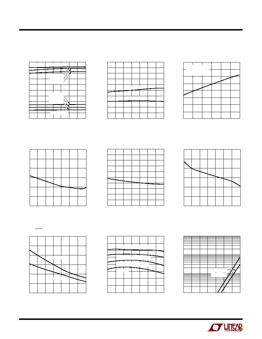
TYPICAL PERFOR
CE
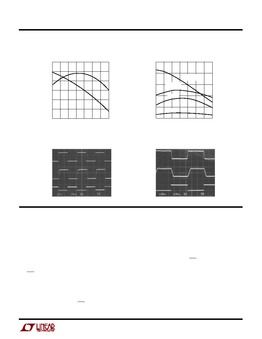
Driver Output Voltage
Driver Disable Threshold
Supply Current in Shutdown
ON/OFF Thresholds
Driver Leakage in Shutdown
Supply Current vs Data Rate
TEMPERATURE (°C)
55
10
DRIVER OUTPUT VOLTAGE (V)
8
4
2
0
10
4
0
50
75
LT1342 · TPC01
6
6
8
2
25
25
100
125
OUTPUT HIGH
OUTPUT LOW
R
L
= 3k
V
CC
= 5V
V
CC
= 4.5V
V
CC
= 5.5V
V
CC
= 4.5V
V
CC
= 5V
V
CC
= 5.5V
TEMPERATURE (°C)
55
0.50
THRESHOLD VOLTAGE (V)
0.75
1.25
1.50
1.75
3.00
2.25
0
50
75
LT1342 · TPC02
1.00
2.50
2.75
2.00
25
25
100
125
INPUT HIGH
INPUT LOW
Receiver Input Thresholds
DATA RATE (kBAUD)
0
0
SUPPLY CURRENT (mA)
20
30
40
60
25
50
125
150
LT1342 · TPC03
70
80
50
10
75
100
3DRIVERS ACTIVE
R
L
= 3k
C
L
= 2500pF
TEMPERATURE (°C)
55
0
SUPPLY CURRENT (mA)
2
5
0
50
75
LT1342 · TPC05
1
4
3
25
25
100
125
TEMPERATURE (°C)
55
THRESHOLD VOLTAGE (V)
2.0
2.5
3.0
25
75
LT1342 · TPC06
1.5
1.0
25
0
50
100
125
0.5
0
TEMPERATURE (°C)
55
THRESHOLD VOLTAGE (V)
2.0
2.5
3.0
25
75
LT1342 · TPC07
1.5
1.0
25
0
50
100
125
0.5
0
ON THRESHOLD
OFF THRESHOLD
TEMPERATURE (°C)
0
SUPPLY CURRENT (mA)
10
15
20
30
LT1341 · TPC08
35
40
25
5
55
0
50
75
25
25
100
125
NO LOAD
1DRIVER LOADED R
L
= 3k
2DRIVERS LOADED R
L
= 3k
3DRIVERS LOADED R
L
= 3k
Supply Current
TEMPERATURE (°C)
0.1
LEAKAGE CURRENT (
µ
A)
10
100
LT1342 · TPC09
1
55
0
50
75
25
25
100
125
V
OUT
= 30V
V
OUT
= 30V
TEMPERATURE (°C)
55
SUPPLY CURRENT (
µ
A)
100
125
150
25
75
LT1342 · TPC04
75
50
25
0
50
100
125
25
0
Supply Current in Driver Disable
5
LT1342
C
C
HARA TERISTICS
U
W
A
TYPICAL PERFOR
CE
Receiver Output Waveforms
Receiver Short-Circuit Current
Driver Output Waveforms
DRIVER OUTPUT
R
L
= 3k
C
L
= 2500pF
INPUT
DRIVER OUTPUT
R
L
= 3k
PI FU CTIO S
U
U
U
V
CC
: 5V Input Supply Pin. This pin should be decoupled
with a 0.1
µ
F ceramic capacitor close to the package pin.
Insufficient supply bypassing can result in low output
drive levels and erratic charge pump operation.
V
L
: 3V Logic Supply Pin. Provides power to the receiver
outputs. Decouple with a 0.1
µ
F ceramic capacitor.
GND: Ground Pin.
ON/OFF: A TTL/CMOS Compatible Operating Mode Con-
trol. A logic low puts the device in the low power shutdown
mode. Drivers and receivers assume a high impedance
state in shutdown. The transceiver consumes almost no
supply current while in shutdown. A logic high fully
enables the transceiver. An ON/OFF logic low signal super-
sedes the state of the DRIVER DISABLE pin.
DRIVER DISABLE: This pin provides an alternate control
for the charge pump and RS232 drivers. A logic high on
this pin shuts down the charge pump and places all drivers
in a high impedance state. All five receivers remain active
under these conditions. Floating the DRIVER DISABLE pin
or driving it to a logic low level fully enables the trans-
ceiver. A logic low on the ON/OFF pin supersedes the state
of the DRIVER DISABLE pin. Supply current drops to 3mA
when in driver disable mode.
V
+
: Positive Supply Output (RS232 Drivers). V
+
2V
CC
1.5V. This pin requires an external charge storage capaci-
tor C
0.1
µ
F, tied to ground or V
CC
. With multiple
transceivers, the V
+
and V
pins may be paralleled into
common charge storage capacitors. Larger value capaci-
tors may be used to reduce supply ripple.
LT1342 · TPC13
Driver Short-Circuit Current
RX5 OUTPUT
C
L
= 50pF
RX1 TO RX4
OUTPUT
C
L
= 50pF
INPUT
LT1342 · TPC12
V
L
= 3V
TEMPERATURE (
°
C)
55
SHORT-CIRCUIT CURRENT (mA)
20
25
30
25
75
LT1342 · TPC10
15
10
25
0
50
100
125
5
0
I
SC
+
I
SC
TEMPERATURE (
°
C)
55
0
SHORT-CIRCUIT CURRENT (mA)
20
50
0
50
75
LT1342 · TPC11
10
40
30
25
25
100
125
RX1 TO RX4
I
SC
+
RX1 TO RX4
I
SC
RX5 I
SC
RX5 I
SC
+