1
LT1374
4.5A, 500kHz Step-Down
Switching Regulator
s
Constant 500kHz Switching Frequency
s
Easily Synchronizable
s
Uses All Surface Mount Components
s
Inductor Size Reduced to 1.8
µ
H
s
Saturating Switch Design: 0.07
s
Effective Supply Current: 2.5mA
s
Shutdown Current: 20
µ
A
s
Cycle-by-Cycle Current Limiting
The LT
Æ
1374 is a 500kHz monolithic buck mode switching
regulator. A 4.5A switch is included on the die along with
all the necessary oscillator, control and logic circuitry. High
switching frequency allows a considerable reduction in the
size of external components. The topology is current mode
for fast transient response and good loop stability. Both
fixed output voltage and adjustable parts are available.
A special high speed bipolar process and new design tech-
niques achieve high efficiency at high switching frequency.
Efficiency is maintained over a wide output current range
by using the output to bias the circuitry and by utilizing a
supply boost capacitor to saturate the power switch.
The LT1374 fits into standard 7-pin DD, TO-220 and fused
lead SO-8 packages. Full cycle-by-cycle short-circuit
protection and thermal shutdown are provided. Standard
surface mount external parts are used, including the
inductor and capacitors. There is the optional function of
shutdown or synchronization. A shutdown signal reduces
supply current to 20
µ
A. Synchronization allows an exter-
nal logic level signal to increase the internal oscillator from
580kHz to 1MHz.
, LTC and LT are registered trademarks of Linear Technology Corporation.
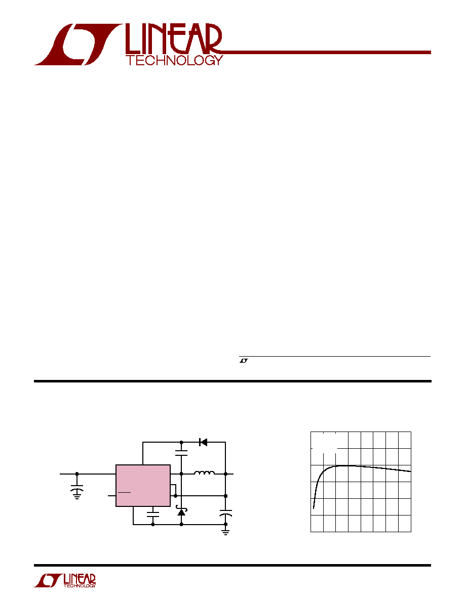
5V Buck Converter
LOAD CURRENT (A)
0
EFFICIENCY (%)
100
95
90
85
80
75
70
2.0
2.5
3.0
3.5
1374 TA02
0.5
1.0
1.5
4.0
V
OUT
= 5V
V
IN
= 10V
L = 10
µ
H
Efficiency vs Load Current
BOOST
LT1374-5
V
IN
SHDN
OUTPUT**
5V, 4.25A
* RIPPLE CURRENT RATING
I
OUT
/2
** INCREASE L1 TO 10
µ
H FOR LOAD CURRENTS ABOVE 3.5A AND TO 20
µ
H ABOVE 4A
SEE APPLICATIONS INFORMATION
INPUT
6V TO 25V
1374 TA01
C2
0.27
µ
F
C
C
1.5nF
D1
MBRS330T3
C1
100
µ
F, 10V
SOLID
TANTALUM
C3*
10
µ
F TO
50
µ
F
DEFAULT
= ON
D2
1N914
L1**
5
µ
H
V
SW
SENSE
BIAS
GND
V
C
+
+
s
Portable Computers
s
Battery-Powered Systems
s
Battery Chargers
s
Distributed Power
FEATURES
DESCRIPTIO
U
APPLICATIO S
U
TYPICAL APPLICATIO
U
2
LT1374
ABSOLUTE
M
AXI
M
U
M
RATINGS
W
W
W
U
Input Voltage
LT1374 ............................................................... 25V
LT1374HV .......................................................... 32V
BOOST Pin Voltage ................................................. 38V
BOOST Pin Above Input Voltage ............................. 15V
SHDN Pin Voltage ..................................................... 7V
BIAS Pin Voltage ...................................................... 7V
FB Pin Voltage (Adjustable Part) ............................ 3.5V
FB Pin Current (Adjustable Part) ............................ 1mA
SENSE Voltage (Fixed 5V Part) ................................. 7V
SYNC Pin Voltage ..................................................... 7V
Operating Junction Temperature Range
LT1374C ............................................... 0
∞
C to 125
∞
C
LT1374I ........................................... ≠ 40
∞
C to 125
∞
C
Storage Temperature Range ................ ≠ 65
∞
C to 150
∞
C
Lead Temperature (Soldering, 10 sec)................. 300
∞
C
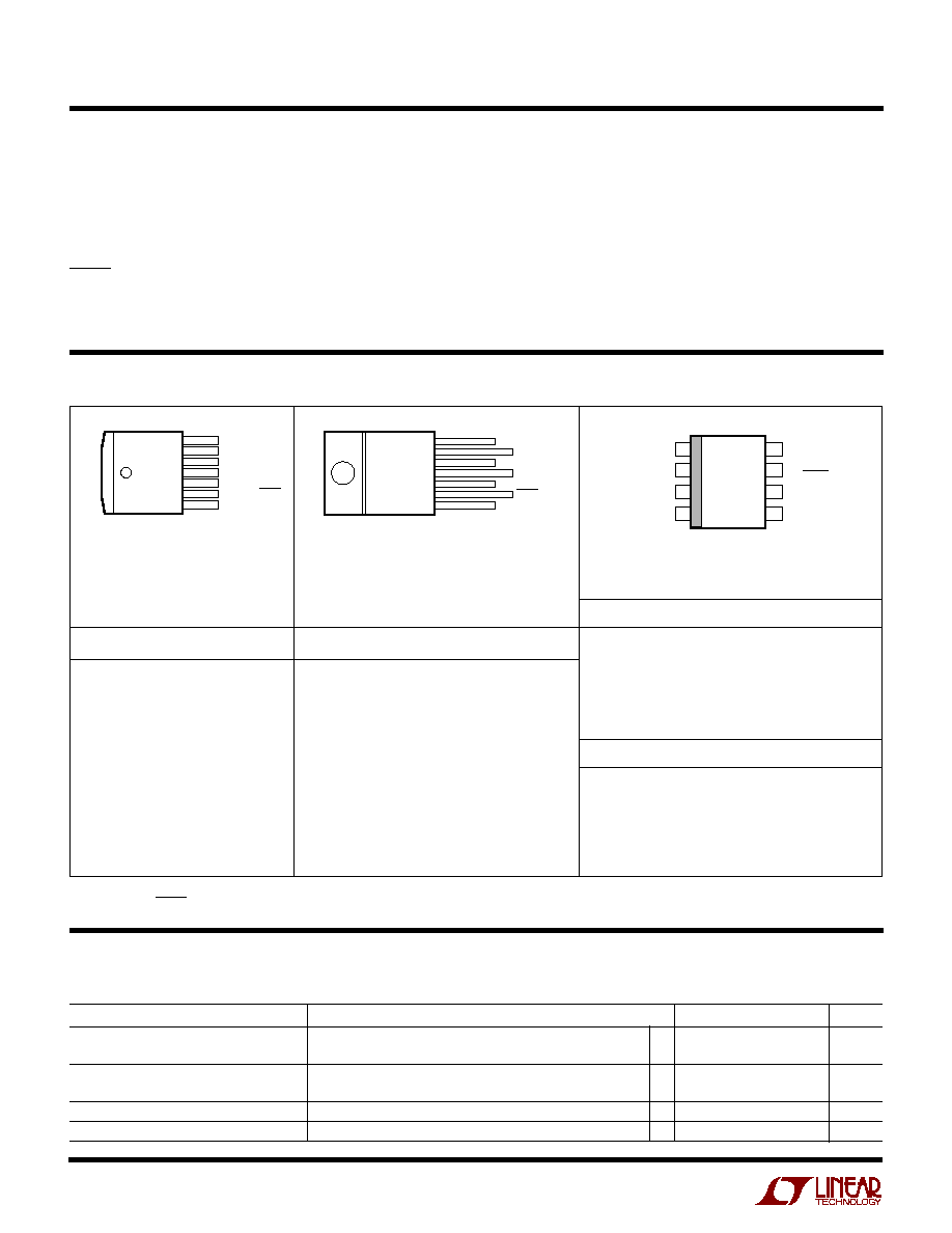
PACKAGE/ORDER I
N
FOR
M
ATIO
N
W
U
U
R PACKAGE
7-LEAD PLASTIC DD
FRONT VIEW
TAB
IS
GND
FB OR SENSE*
BOOST
V
IN
GND
V
SW
SYNC OR SHDN*
V
C
7
6
5
4
3
2
1
1
2
3
4
8
7
6
5
TOP VIEW
S8 PACKAGE
8-LEAD PLASTIC SO
V
IN
BOOST
FGND
V
SW
V
C
BIAS
SYNC
OR SHDN*
FB OR
SENSE*
JA
= 80
∞
C/ W WITH FUSED (FGND) GROUND PIN
CONNECTED TO GROUND PLANE OR LARGE LANDS
ORDER PART NUMBER
LT1374IS8
LT1374IS8-5
LT1374IS8-SYNC
LT1374IS8-5 SYNC
LT1374HVIS8
LT1374CS8
LT1374CS8-5
LT1374CS8-SYNC
LT1374CS8-5 SYNC
LT1374HVCS8
S8 PART MARKING
T
JMAX
= 125
∞
C,
JA
= 30
∞
C/ W
WITH PACKAGE SOLDERED TO 0.5 SQUARE INCH
COPPER AREA OVER BACKSIDE GROUND PLANE
OR INTERNAL POWER PLANE.
JA
CAN VARY
FROM 20
∞
C/W TO > 40
∞
C/W DEPENDING ON
MOUNTING TECHNIQUES
ORDER PART NUMBER
ORDER PART NUMBER
LT1374CR
LT1374CR-5
LT1374CR-SYNC
LT1374CR-5 SYNC
LT1374HVCR
LT1374IR
LT1374IR-5
LT1374IR-SYNC
LT1374IR-5 SYNC
LT1374HVIR
LT1374CT7
LT1374CT7-5
LT1374IT7
LT1374IT7-5
T7 PACKAGE
7-LEAD PLASTIC TO-220
FB OR SENSE*
BOOST
V
IN
GND
V
SW
SHDN
V
C
FRONT VIEW
TAB
IS
GND
7
6
5
4
3
2
1
T
JMAX
= 125
∞
C
,
JA
= 50
∞
C/ W,
JC
= 4
∞
C/ W
*Default is the adjustable output voltage device with FB pin and shutdown function. Option -5 replaces FB with SENSE pin for fixed 5V output applications.
-SYNC replaces SHDN with SYNC pin for applications requiring synchronization. Consult factory for Military grade parts.
1374
13745
1374SN
3745SN
1374HV
1374I
1374I5
374ISN
74I5SN
1374HVI
(Note 1)
PARAMETER
CONDITIONS
MIN
TYP
MAX
UNITS
Feedback Voltage (Adjustable)
2.39
2.42
2.45
V
All Conditions
q
2.36
2.48
V
Sense Voltage (Fixed 5V)
4.94
5.0
5.06
V
All Conditions
q
4.90
5.10
V
SENSE Pin Resistance
7
10
14
k
Reference Voltage Line Regulation
5V
V
IN
25V (5V
V
IN
32V for LT1374HV)
0.01
0.03
%/V
The
q
denotes specifications which apply over the full operating tempera-
ture range, otherwise specifications are at T
J
= 25
∞
C. V
IN
= 15V, V
C
= 1.5V, Boost = V
IN
+ 5V, switch open, unless otherwise noted.
ELECTRICAL CHARACTERISTICS
3
LT1374
PARAMETER
CONDITIONS
MIN
TYP
MAX
UNITS
Feedback Input Bias Current
q
0.5
2
µ
A
Error Amplifier Voltage Gain
(Notes 2, 8)
200
400
Error Amplifier Transconductance
I (V
C
) =
±
10
µ
A (Note 8)
1500
2000
2700
µ
Mho
q
1000
3100
µ
Mho
V
C
Pin to Switch Current Transconductance
5.3
A/ V
Error Amplifier Source Current
V
FB
= 2.1V or V
SENSE
= 4.4V
q
140
225
320
µ
A
Error Amplifier Sink Current
V
FB
= 2.7V or V
SENSE
= 5.6V
q
140
225
320
µ
A
V
C
Pin Switching Threshold
Duty Cycle = 0
0.9
V
V
C
Pin High Clamp
2.1
V
Switch Current Limit
V
C
Open, V
FB
= 2.1V or V
SENSE
= 4.4V, DC
50%
q
4.5
6
8.5
A
Slope Compensation (Note 9)
DC = 80%
0.8
A
Switch On Resistance (Note 7)
I
SW
= 4.5A
0.07
0.1
q
0.13
Maximum Switch Duty Cycle
V
FB
= 2.1V or V
SENSE
= 4.4V
90
93
%
q
86
93
%
Switch Frequency
V
C
Set to Give 50% Duty Cycle
460
500
540
kHz
q
440
560
kHz
Switch Frequency Line Regulation
5V
V
IN
25V, (5V
V
IN
32V for LT1374HV)
q
0
0.15
%/ V
Frequency Shifting Threshold on FB Pin
f = 10kHz
q
0.8
1.0
1.3
V
Minimum Input Voltage (Note 3)
q
5.0
5.5
V
Minimum Boost Voltage (Note 4)
I
SW
4.5A
q
2.3
3.0
V
Boost Current (Note 5)
I
SW
= 1A
q
20
35
mA
I
SW
= 4.5A
q
90
140
mA
V
IN
Supply Current (Note 6)
V
BIAS
= 5V
q
0.9
1.4
mA
BIAS Supply Current (Note 6)
V
BIAS
= 5V
q
3.2
4.0
mA
Shutdown Supply Current
V
SHDN
= 0V, V
IN
25V, V
SW
= 0V, V
C
Open
20
50
µ
A
q
75
µ
A
V
SHDN
= 0V, V
IN
32V, V
SW
= 0V, V
C
Open
30
75
µ
A
q
100
µ
A
Lockout Threshold
V
C
Open
q
2.3
2.38
2.46
V
Shutdown Thresholds
V
C
Open Device Shutting Down
q
0.13
0.37
0.60
V
Device Starting Up
q
0.25
0.45
0.7
V
Synchronization Threshold
q
1.5
2.2
V
Synchronizing Range
580
1000
kHz
SYNC Pin Input Resistance
40
k
Note 1: Absolute Maximum Ratings are those values beyond which the life
of a device may be impaired.
Note 2: Gain is measured with a V
C
swing equal to 200mV above the
switching threshold level to 200mV below the upper clamp level.
Note 3: Minimum input voltage is not measured directly, but is guaranteed
by other tests. It is defined as the voltage where internal bias lines are still
regulated so that the reference voltage and oscillator frequency remain
constant. Actual minimum input voltage to maintain a regulated output will
depend on output voltage and load current. See Applications Information.
Note 4: This is the minimum voltage across the boost capacitor needed to
guarantee full saturation of the internal power switch.
Note 5: Boost current is the current flowing into the boost pin with the pin
held 5V above input voltage. It flows only during switch on time.
Note 6: V
IN
supply current is the current drawn when the BIAS pin is held
at 5V and switching is disabled. If the BIAS pin is unavailable or open
circuit, the sum of V
IN
and BIAS supply currents will be drawn by the V
IN
pin.
Note 7: Switch on resistance is calculated by dividing V
IN
to V
SW
voltage
by the forced current (4.5A). See Typical Performance Characteristics for
the graph of switch voltage at other currents.
Note 8: Transconductance and voltage gain refer to the internal amplifier
exclusive of the voltage divider. To calculate gain and transconductance,
refer to the SENSE pin on the fixed voltage parts. Divide values shown by
the ratio V
OUT
/2.42.
Note 9: Slope compensation is the current subtracted from the switch
current limit at 80% duty cycle. See Maximum Output Load Current in the
Applications Information section for further details.
The
q
denotes specifications which apply over the full operating tempera-
ture range, otherwise specifications are at T
J
= 25
∞
C. V
IN
= 15V, V
C
= 1.5V, Boost = V
IN
+ 5V, switch open, unless otherwise noted.
ELECTRICAL CHARACTERISTICS
4
LT1374
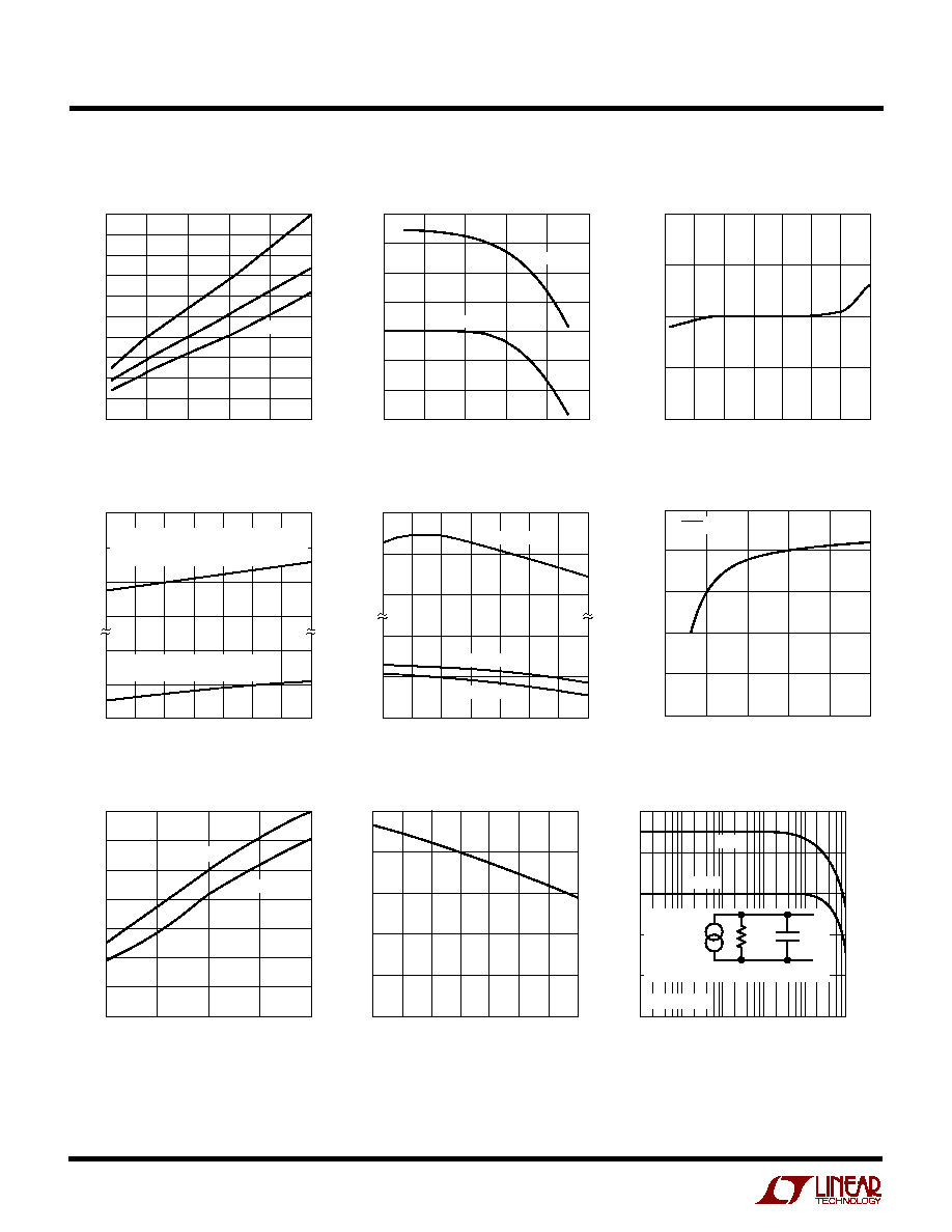
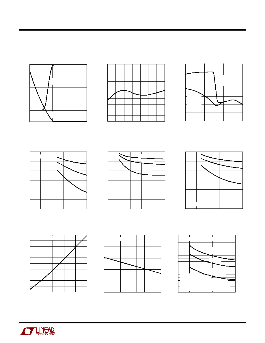
TYPICAL PERFOR
M
A
N
CE CHARACTERISTICS
U
W
Switch Voltage Drop
SWITCH CURRENT (A)
0
SWITCH VOLTAGE (mV)
250
200
400
125
∞
C
25
∞
C
350
300
4
5
1374 G18
150
100
50
0
1
2
3
500
450
≠ 40
∞
C
Feedback Pin Voltage
TEMPERATURE (
∞
C)
≠ 50
2.430
2.425
2.420
2.415
2.410
100
1374 G03
≠25
0
25
50
75
125
FEEDBACK VOLTAGE (V)
Switch Peak Current Limit
DUTY CYCLE (%)
0
SWITCH PEAK CURRENT (A)
6.5
6.0
5.5
5.0
4.5
4.0
3.5
3.0
80
1374 G02
20
40
60
100
TYPICAL
MINIMUM
Shutdown Pin Bias Current
TEMPERATURE (
∞
C)
≠50
500
400
300
200
8
4
0
25
75
1374 G04
≠25
0
50
100
125
CURRENT (
µ
A)
CURRENT REQUIRED TO FORCE SHUTDOWN
(FLOWS OUT OF PIN). AFTER SHUTDOWN,
CURRENT DROPS TO A FEW
µ
A
AT 2.38V STANDBY THRESHOLD
(CURRENT FLOWS OUT OF PIN)
Standby and Shutdown Thresholds
Shutdown Supply Current
JUNCTION TEMPERATURE (
∞
C)
≠50
2.40
2.36
2.32
0.8
0.4
0
25
75
1374 G05
≠25
0
50
100
125
SHUTDOWN PIN VOLTAGE (V)
STANDBY
START-UP
SHUTDOWN
INPUT VOLTAGE (V)
0
INPUT SUPPLY CURRENT (
µ
A)
25
20
15
10
5
0
5
10
15
20
1374 G06
25
V
SHDN
= 0V
Shutdown Supply Current
SHUTDOWN VOLTAGE (V)
0
INPUT SUPPLY CURRENT (
µ
A)
70
60
50
40
30
20
10
0
0.1
0.2
0.3
0.4
1374 G07
V
IN
= 25V
V
IN
= 10V
Error Amplifier Transconductance
FREQUENCY (Hz)
GAIN (
µ
Mho)
PHASE (DEG)
3000
2500
2000
1500
1000
500
200
150
100
50
0
≠50
100
10k
100k
10M
1374 G09
1k
1M
GAIN
PHASE
ERROR AMPLIFIER EQUIVALENT CIRCUIT
R
OUT
200k
C
OUT
12pF
V
C
R
LOAD
= 50
V
FB
2
◊
10
≠3
)
(
Error Amplifier Transconductance
JUNCTION TEMPERATURE (
∞
C)
≠50
TRANSCONDUCTANCE (
µ
Mho)
2500
2000
1500
1000
500
0
0
50
75
1374 G08
≠25
25
100
125
5
LT1374
TYPICAL PERFOR
M
A
N
CE CHARACTERISTICS
U
W
FEEDBACK PIN VOLTAGE (V)
0
SWITCHING FREQUENCY (kHz) OR CURRENT (
µ
A) 500
400
300
200
100
0
2.0
1374 G10
0.5
1.0
1.5
2.5
SWITCHING
FREQUENCY
FEEDBACK PIN
CURRENT
Frequency Foldback
LOAD CURRENT (mA)
1
5.8
INPUT VOLTAGE (V)
6.0
6.2
6.4
10
100
1000
1374 G12
5.6
5.4
5.2
5.0
MINIMUM
RUNNING
VOLTAGE
MINIMUM
STARTING
VOLTAGE
Minimum Input Voltage
with 5V Output
TEMPERATURE (
∞
C)
≠ 50
550
540
530
520
510
500
490
480
470
460
450
100
1374 G11
≠25
0
25
50
75
125
FREQUENCY (kHz)
Switching Frequency
Maximum Load Current
at V
OUT
= 10V
INPUT VOLTAGE (V)
0
CURRENT (A)
4.5
4.0
3.5
3.0
5
10
15
20
1374 G13
25
L = 20
µ
H
L = 10
µ
H
L = 5
µ
H
V
OUT
= 10V
Maximum Load Current
at V
OUT
= 3.3V
INPUT VOLTAGE (V)
0
CURRENT (A)
4.5
4.0
3.5
3.0
5
10
15
20
1374 G14
25
L = 20
µ
H
L = 10
µ
H
L = 5
µ
H
V
OUT
= 3.3V
Maximum Load Current
at V
OUT
= 5V
INPUT VOLTAGE (V)
0
CURRENT (A)
4.5
4.0
3.5
3.0
5
10
15
20
1374 G15
25
L = 20
µ
H
L = 10
µ
H
L = 5
µ
H
V
OUT
= 5V
BOOST Pin Current
SWITCH CURRENT (A)
0
0
BOOST PIN CURRENT (mA)
10
20
40
30
60
50
1
2
3
4
5
1374 G16
80
70
100
90
DUTY CYCLE = 100%
Inductor Core Loss
INDUCTANCE (
µ
H)
0
5
CORE LOSS (W)
CORE LOSS (% OF 5W LOAD)
1.0
0.1
0.01
0.001
10
15
20
20
12
8
4
2
1.2
0.8
0.4
0.2
0.12
0.08
0.04
0.02
25
1374 G01
TYPE 52
POWDERED IRON
Kool M
µ
Æ
PERMALLOY
µ
= 125
V
OUT
= 5V, V
IN
= 10V, I
OUT
= 1A
CORE LOSS IS
INDEPENDENT OF LOAD
CURRENT UNTIL LOAD CURRENT FALLS
LOW ENOUGH FOR CIRCUIT TO GO INTO
DISCONTINUOUS MODE
V
C
Pin Shutdown Threshold
JUNCTION TEMPERATURE (
∞
C)
≠50
1.4
1.2
1.0
0.8
0.6
0.4
100
1374 G11
≠25
0
25
50
75
125
THRESHOLD VOLTAGE (V)
SHUTDOWN
Kool M
µ
is a registered trademark of Magnetics, Inc.