 | –≠–ª–µ–∫—Ç—Ä–æ–Ω–Ω—ã–π –∫–æ–º–ø–æ–Ω–µ–Ω—Ç: LT1376I | –°–∫–∞—á–∞—Ç—å:  PDF PDF  ZIP ZIP |
1
LT1375/LT1376
1.5A, 500kHz Step-Down
Switching Regulators
s
Constant 500kHz Switching Frequency
s
Easily Synchronizable
s
Uses All Surface Mount Components
s
Inductor Size Reduced to 5
µ
H
s
Saturating Switch Design: 0.4
s
Effective Supply Current: 2.5mA
s
Shutdown Current: 20
µ
A
s
Cycle-by-Cycle Current Limiting
s
Portable Computers
s
Battery-Powered Systems
s
Battery Charger
s
Distributed Power
The LT
Æ
1375/LT1376 are 500kHz monolithic buck mode
switching regulators. A 1.5A switch is included on the die
along with all the necessary oscillator, control and logic
circuitry. High switching frequency allows a considerable
reduction in the size of external components. The topology
is current mode for fast transient response and good loop
stability. Both fixed output voltage and adjustable parts are
available.
A special high speed bipolar process and new design
techniques achieve high efficiency at high switching fre-
quency. Efficiency is maintained over a wide output cur-
rent range by using the output to bias the circuitry and by
utilizing a supply boost capacitor to saturate the power
switch. A shutdown signal will reduce supply current to
20
µ
A on both parts. The LT1375 can be externally syn-
chronized from 550kHz to 1MHz with logic level inputs.
The LT1375/LT1376 fit into standard 8-pin PDIP and SO
packages, as well as a fused lead 16-pin SO with much
lower thermal resistance. Full cycle-by-cycle short-cir-
cuit protection and thermal shutdown are provided.
Standard surface mount external parts are used, includ-
ing the inductor and capacitors.
For low input voltage applications with 3.3V output, see
LT1507. This is a functionally identical part that can
operate with input voltages between 4.5V and 12V.
, LTC and LT are registered trademarks of Linear Technology Corporation.
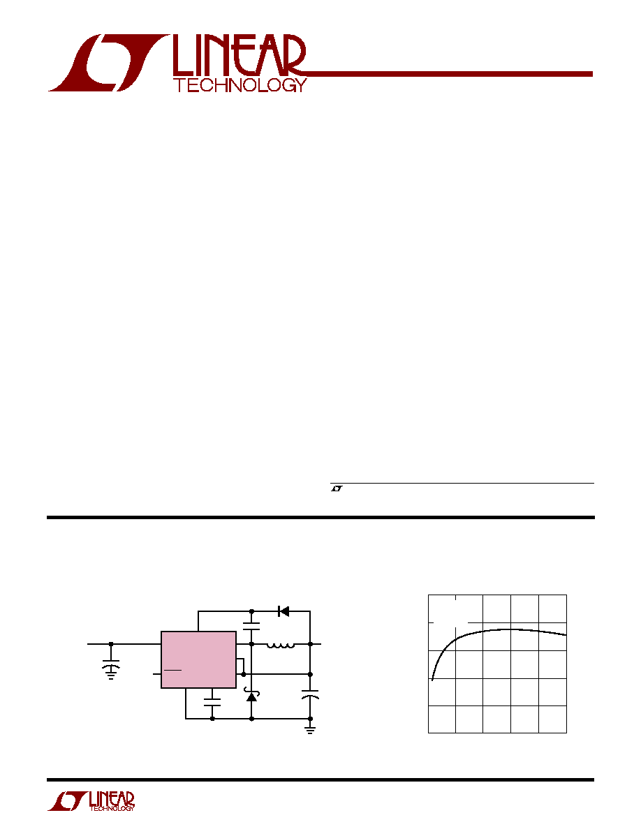
5V Buck Converter
LOAD CURRENT (A)
0
EFFICIENCY (%)
100
90
80
70
60
50
1.00
1375/76 TA02
0.25
0.50
0.75
1.25
V
OUT
= 5V
V
IN
= 10V
L = 10
µ
H
Efficiency vs Load Current
BOOST
LT1376-5
V
IN
OUTPUT**
5V, 1.25A
* RIPPLE CURRENT
I
OUT
/2
** INCREASE L1 TO 10
µ
H FOR LOAD CURRENTS ABOVE 0.6A AND TO 20
µ
H ABOVE 1A
FOR INPUT VOLTAGE BELOW 7.5V, SOME RESTRICTIONS MAY APPLY.
SEE APPLICATIONS INFORMATION.
INPUT
6V
TO 25V
1375/76 TA01
C2
0.1
µ
F
C
C
3.3nF
D2
1N5818
C1
100
µ
F, 10V
SOLID
TANTALUM
C3*
10
µ
F TO
50
µ
F
D2
1N914
L1**
5
µ
H
V
SW
FB
BIAS
GND
V
C
DEFAULT
= ON
SHDN
+
+
FEATURES
APPLICATIO S
U
DESCRIPTIO
U
TYPICAL APPLICATIO
U
2
LT1375/LT1376
ABSOLUTE
M
AXI
M
U
M
RATINGS
W
W
W
U
Input Voltage
LT1375/LT1376 .................................................. 25V
LT1375HV/LT1376HV ........................................ 30V
BOOST Pin Voltage
LT1375/LT1376 .................................................. 35V
LT1375HV/LT1376HV ........................................ 40V
SHDN Pin Voltage ..................................................... 7V
BIAS Pin Voltage ...................................................... 7V
FB Pin Voltage (Adjustable Part) ............................ 3.5V
FB Pin Current (Adjustable Part) ............................ 1mA
Sense Voltage (Fixed 5V Part) .................................. 7V
SYNC Pin Voltage ..................................................... 7V
Operating Ambient Temperature Range
LT1375C/LT1376C ................................. 0
∞
C to 70
∞
C
LT1375I/LT1376I ............................... ≠ 40
∞
C to 85
∞
C
Operating Junction Temperature Range
LT1375C/LT1376C ............................... 0
∞
C to 125
∞
C
LT1375I/LT1376I ............................. ≠ 40
∞
C to 125
∞
C
Storage Temperature Range ................ ≠ 65
∞
C to 150
∞
C
Lead Temperature (Soldering, 10 sec)................. 300
∞
C
(Note 1)
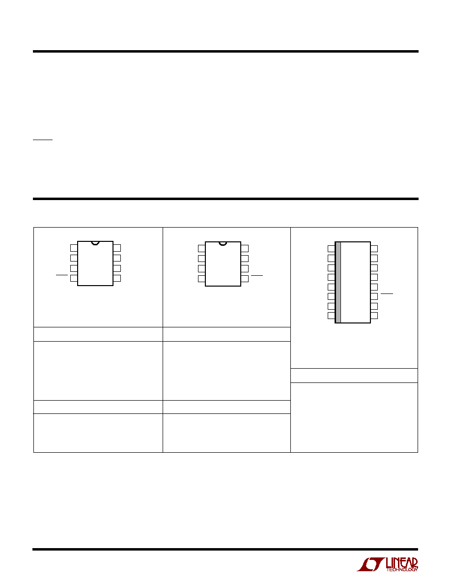
PACKAGE/ORDER I
N
FOR
M
ATIO
N
W
U
U
TOP VIEW
S PACKAGE
16-LEAD PLASTIC NARROW SO
1
2
3
4
5
6
7
8
16
15
14
13
12
11
10
9
GND
NC
BOOST
V
IN
V
SW
BIAS
NC
GND
GND
NC
V
C
FB/SENSE
GND
SHDN
NC
GND
ORDER PART NUMBER
JA
= 50
∞
C/ W WITH FUSED CORNER PINS
CONNECTED TO GROUND PLANE OR LARGE
LANDS
1
2
3
4
8
7
6
5
TOP VIEW
BOOST
V
IN
V
SW
BIAS
N8 PACKAGE
8-LEAD PDIP
S8 PACKAGE
8-LEAD PLASTIC SO
V
C
FB/SENSE
GND
SHDN
JA
= 100
∞
C/ W (N8)
JA
= 120
∞
C/ W TO 150
∞
C/W DEPENDING ON
PC BOARD LAYOUT (S8)
1
2
3
4
8
7
6
5
TOP VIEW
V
C
FB/SENSE
GND
SYNC
N8 PACKAGE
8-LEAD PDIP
S8 PACKAGE
8-LEAD PLASTIC SO
BOOST
V
IN
V
SW
SHDN
JA
= 100
∞
C/ W (N8)
JA
= 120
∞
C/ W TO 150
∞
C/W DEPENDING ON
PC BOARD LAYOUT (S8)
LT1375CN8
LT1375CN8-5
LT1375CS8
LT1375CS8-5
LT1375HVCS8
ORDER PART NUMBER
ORDER PART NUMBER
LT1375IN8
LT1375IN8-5
LT1375IS8
LT1375IS8-5
LT1375HVIS8
LT1376CN8
LT1376CN8-5
LT1376CS8
LT1376CS8-5
LT1376HVCS8
LT1376IN8
LT1376IN8-5
LT1376IS8
LT1376IS8-5
LT1376HVIS8
S8 PART MARKING
S8 PART MARKING
1375I
1375I5
375HVI
1375
13755
1375HV
1376
13765
1376HV
1376I
1376I5
376HVI
LT1376CS
LT1376IS
LT1376HVCS
LT1376HVIS
Consult factory for Military grade parts.
3
LT1375/LT1376
ELECTRICAL CHARACTERISTICS
The
q
denotes specifications which apply over the full operating
temperature range, otherwise specifications are at T
A
= 25
∞
C. T
J
= 25
∞
C, V
IN
= 15V, V
C
= 1.5V, boost open, switch open,
unless otherwise noted.
PARAMETER
CONDITIONS
MIN
TYP
MAX
UNITS
Reference Voltage (Adjustable)
2.39
2.42
2.45
V
All Conditions
q
2.36
2.48
V
Sense Voltage (Fixed 5V)
4.94
5.0
5.06
V
All Conditions
q
4.90
5.10
V
Sense Pin Resistance
7
10
14
k
Reference Voltage Line Regulation
5V
V
IN
25V
0.01
0.03
%/ V
5V
V
IN
30V (LT1375HV/LT1376HV)
0.01
0.03
%/V
Feedback Input Bias Current
q
0.5
1.5
µ
A
Error Amplifier Voltage Gain
V
SHDN
= 1V (Notes 2, 8)
200
400
Error Amplifier Transconductance
V
SHDN
= 1V,
I (V
C
) =
±
10
µ
A (Note 8)
1500
2000
2700
µ
Mho
q
1100
3000
µ
Mho
V
C
Pin to Switch Current Transconductance
2
A/ V
Error Amplifier Source Current
V
SHDN
= 1V, V
FB
= 2.1V or V
SENSE
= 4.4V
q
150
225
320
µ
A
Error Amplifier Sink Current
V
SHDN
= 1V, V
FB
= 2.7V or V
SENSE
= 5.6V
2
mA
V
C
Pin Switching Threshold
Duty Cycle = 0
0.9
V
V
C
Pin High Clamp
V
SHDN
= 1V
2.1
V
Switch Current Limit
V
C
Open, V
FB
= 2.1V or V
SENSE
= 4.4V,
V
BOOST
= V
IN
+ 5V
DC
50%
q
1.50
2
3
A
DC = 80%
q
1.35
3
A
Switch On Resistance (Note 6)
I
SW
= 1.5A, V
BOOST
= V
IN
+ 5V
0.3
0.4
q
0.5
Maximum Switch Duty Cycle
V
FB
= 2.1V or V
SENSE
= 4.4V
90
93
%
≠ 40
∞
C
T
J
125
∞
C
86
93
%
T
J
= 150
∞
C
85
93
%
Switch Frequency
V
C
Set to Give 50% Duty Cycle
460
500
540
kHz
≠ 25
∞
C
T
J
125
∞
C
440
560
kHz
T
J
≠ 25
∞
C
440
570
kHz
Switch Frequency Line Regulation
5V
V
IN
25V
q
0.05
0.15
%/ V
5V
V
IN
30V (LT1375HV/LT1376HV)
q
0.05
0.15
%/V
Frequency Shifting Threshold on FB Pin
f = 10kHz
q
0.8
1.0
1.3
V
Minimum Input Voltage (Note 3)
q
5.0
5.5
V
Minimum Boost Voltage (Note 4)
I
SW
1.5A
q
3
3.5
V
Boost Current (Note 5)
V
BOOST
= V
IN
+ 5V
I
SW
= 500mA
q
12
22
mA
I
SW
= 1.5A
q
25
35
mA
Input Supply Current (Note 6)
V
BIAS
= 5V
q
0.9
1.4
mA
Output Supply Current (Note 6)
V
BIAS
= 5V
q
3.2
4.0
mA
Shutdown Supply Current
V
SHDN
= 0V, V
IN
25V, V
SW
= 0V, V
C
Open
15
50
µ
A
q
75
µ
A
V
SHDN
= 0V, V
IN
30V, V
SW
= 0V, V
C
Open
(LT1375HV/LT1376HV)
20
75
µ
A
q
100
µ
A
Lockout Threshold
V
C
Open
q
2.3
2.38
2.46
V
4
LT1375/LT1376
Kool M
µ
is a registered trademark of Magnetics, Inc.
ELECTRICAL CHARACTERISTICS
Note 1: Absolute Maximum Ratings are those values beyond which the life
of a device may be impaired.
Note 2: Gain is measured with a V
C
swing equal to 200mV above the low
clamp level to 200mV below the upper clamp level.
Note 3: Minimum input voltage is not measured directly, but is guaranteed
by other tests. It is defined as the voltage where internal bias lines are still
regulated so that the reference voltage and oscillator frequency remain
constant. Actual minimum input voltage to maintain a regulated output will
depend on output voltage and load current. See Applications Information.
Note 4: This is the minimum voltage across the boost capacitor needed to
guarantee full saturation of the internal power switch.
Note 5: Boost current is the current flowing into the BOOST pin with the
pin held 5V above input voltage. It flows only during switch-on time.
Note 6: Input supply current is the bias current drawn by the input pin
when the BIAS pin is held at 5V with switching disabled. Output supply
current is the current drawn by the BIAS pin when the bias pin is held at
5V. Total input referred supply current is calculated by summing input
supply current (I
SI
) with a fraction of output supply current (I
SO
):
I
TOT
= I
SI
+ (I
SO
)(V
OUT
/V
IN
)(1.15)
With V
IN
= 15V, V
OUT
= 5V, I
SI
= 0.9mA, I
SO
= 3.6mA, I
TOT
= 2.28mA.
For the LT1375, quiescent current is equal to:
I
TOT
= I
SI
+ I
SO
(1.15)
because the BIAS pin is internally connected to V
IN
.
Note 7: Switch-on resistance is calculated by dividing V
IN
to V
SW
voltage
by the forced current (1.5A). See Typical Performance Characteristics for
the graph of switch voltage at other currents.
Note 8: Transconductance and voltage gain refer to the internal amplifier
exclusive of the voltage divider. To calculate gain and transconductance
refer to sense pin on fixed voltage parts. Divide values shown by the ratio
V
OUT
/2.42.
The
q
denotes specifications which apply over the full operating
temperature range, otherwise specifications are at T
A
= 25
∞
C. T
J
= 25
∞
C, V
IN
= 15V, V
C
= 1.5V, boost open, switch open,
unless otherwise noted.
PARAMETER
CONDITIONS
MIN
TYP
MAX
UNITS
Shutdown Thresholds
V
C
Open
Device Shutting Down
q
0.15
0.37
0.60
V
Device Starting Up
q
0.25
0.45
0.60
V
V
C
Open
LT1375HV/LT1376HV Device Shutting Down
q
0.15
0.37
0.70
V
LT1375HV/LT1376HV Device Starting Up
q
0.25
0.45
0.70
V
Minimum Synchronizing Amplitude (LT1375 Only)
V
IN
= 5V
q
1.5
2.2
V
Synchronizing Range (LT1375 Only)
580
900
kHz
SYNC Pin Input Resistance
40
k
INDUCTANCE (
µ
H)
0
5
CORE LOSS (W)
CORE LOSS (% OF 5W LOAD)
1.0
0.1
0.01
0.001
10
15
20
20
12
8
4
2
1.2
0.8
0.4
0.2
0.12
0.08
0.04
0.02
25
1375/76 G01
TYPE 52
POWDERED IRON
Kool M
µ
Æ
PERMALLOY
µ
= 125
V
OUT
= 5V, V
IN
= 10V, I
OUT
= 1A
CORE LOSS IS
INDEPENDENT OF LOAD
CURRENT UNTIL LOAD CURRENT FALLS
LOW ENOUGH FOR CIRCUIT TO GO INTO
DISCONTINUOUS MODE
Inductor Core Loss
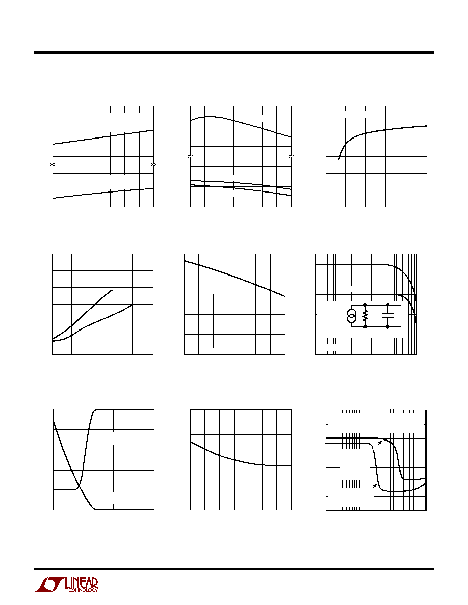
TYPICAL PERFOR
M
A
N
CE CHARACTERISTICS
U
W
DUTY CYCLE (%)
0
SWITCH PEAK CURRENT (A)
2.5
2.0
1.5
1.0
0.5
0
80
1375/76 G08
20
40
60
100
TYPICAL
GUARANTEED MINIMUM
Switch Peak Current Limit
JUNCTION TEMPERATURE (
∞
C)
≠50
2.44
2.43
2.42
2.41
2.40
100
1375/76 G09
≠25
0
25
50
75
125
FEEDBACK VOLTAGE (V)
CURRENT (
µ
A)
2.0
1.5
1.0
0.5
0
VOLTAGE
CURRENT
Feedback Pin Voltage and Current
5
LT1375/LT1376
TYPICAL PERFOR
M
A
N
CE CHARACTERISTICS
U
W
TEMPERATURE (
∞
C)
≠50
500
400
300
200
8
4
0
25
75
1375/76 G04
≠25
0
50
100
125
CURRENT (
µ
A)
CURRENT REQUIRED TO FORCE SHUTDOWN
(FLOWS OUT OF PIN). AFTER SHUTDOWN,
CURRENT DROPS TO A FEW
µ
A
AT 2.38V STANDBY THRESHOLD
(CURRENT FLOWS OUT OF PIN)
Shutdown Pin Bias Current
JUNCTION TEMPERATURE (
∞
C)
≠50
TRANSCONDUCTANCE (
µ
Mho)
2500
2000
1500
1000
500
0
0
50
75
1375/76 G02
≠25
25
100
125
Error Amplifier Transconductance
FREQUENCY (Hz)
GAIN (
µ
Mho)
PHASE (DEG)
3000
2500
2000
1500
1000
500
200
150
100
50
0
≠50
100
10k
100k
10M
1375/76 G03
1k
1M
GAIN
PHASE
ERROR AMPLIFIER EQUIVALENT CIRCUIT
R
OUT
200k
C
OUT
12pF
V
C
R
LOAD
= 50
V
FB 2 ∑
10
≠3
)
(
Error Amplifier Transconductance
Frequency Foldback
LOAD CURRENT (mA)
0
INPUT VOLTAGE (V)
8.5
8.0
7.5
7.0
6.5
6.0
5.5
5.0
10
100
1000
1375/76 G12
MINIMUM INPUT VOLTAGE CAN BE
REDUCED BY ADDING A SMALL EXTERNAL
PNP. SEE APPLICATIONS INFORMATION
MINIMUM
VOLTAGE TO
START WITH
STANDARD
CIRCUIT
MINIMUM VOLTAGE
TO RUN WITH
STANDARD CIRCUIT
LT1376 Minimum Input Voltage
with 5V Output
Shutdown Supply Current
INPUT VOLTAGE (V)
0
INPUT SUPPLY CURRENT (
µ
A)
30
25
20
15
10
5
0
5
10
15
20
1375/76 G06
25
V
SHUTDOWN
= 0V
JUNCTION TEMPERATURE (
∞
C)
≠50
2.40
2.36
2.32
0.8
0.4
0
25
75
1375/76 G05
≠25
0
50
100
125
SHUTDOWN PIN VOLTAGE (V)
STANDBY
START-UP
SHUTDOWN
Standby and Shutdown Thresholds
Shutdown Supply Current
SHUTDOWN VOLTAGE (V)
0
INPUT SUPPLY CURRENT (
µ
A)
150
125
100
75
50
25
0
0.1
0.2
0.3
0.4
1375/76 G07
0.5
V
IN
= 25V
V
IN
= 10V
FEEDBACK PIN VOLTAGE (V)
0
SWITCHING FREQUENCY (kHz) OR CURRENT (
µ
A) 500
400
300
200
100
0
2.0
1375/76 G10
0.5
1.0
1.5
2.5
SWITCHING
FREQUENCY
FEEDBACK PIN
CURRENT
Switching Frequency
JUNCTION TEMPERATURE (
∞
C)
≠50
600
550
500
450
400
100
1375/76 G11
≠25
0
25
50
75
125
FREQUENCY (kHz)