 | ÐлекÑÑоннÑй компоненÑ: LT1395CS6 | СкаÑаÑÑ:  PDF PDF  ZIP ZIP |
139567fb.pm6
1
LT1395/LT1396/LT1397
139567fb
APPLICATIO S
U
FEATURES
TYPICAL APPLICATIO
U
DESCRIPTIO
U
Single/Dual/Quad 400MHz
Current Feedback Amplifier
The LT
®
1395/LT1396/LT1397 are single/dual/quad
400MHz current feedback amplifiers with an 800V/
µ
s slew
rate and the ability to drive up to 80mA of output current.
The LT1395/LT1396/LT1397 operate on all supplies from
a single 4V to
±
6V. At
±
5V, they draw 4.6mA of supply
current per amplifier. The LT1395CS6 also adds a shut-
down pin. When disabled, the LT1395CS6 draws virtually
zero supply current and its output becomes high imped-
ance. The LT1395CS6 will turn on in only 30ns and turn off
in 40ns, making it ideal in spread spectrum and portable
equipment applications.
For space limited applications, the LT1395 is available in
SOT-23 packages. The LT1396 is available in a 3mm
×
3mm
×
0.8mm dual fine pitch leadless package (DNF).
The LT1395/LT1396/LT1397 are manufactured on Linear
Technology's proprietary complementary bipolar process.
They have standard single/dual/quad pinouts and they are
optimized for use on supply voltages of
±
5V.
s
400MHz Bandwidth on
±
5V (A
V
= 1)
s
350MHz Bandwidth on
±
5V (A
V
= 2, 1)
s
0.1dB Gain Flatness: 100MHz (A
V
= 1, 2 and 1)
s
Tiny 3mm
×
3mm
×
0.8mm DFN Package (LT1396)
s
High Slew Rate: 800V/
µ
s
s
Wide Supply Range:
±
2V(4V) to
±
6V(12V)
s
80mA Output Current
s
Low Supply Current: 4.6mA/Amplifier
s
LT1395: SO-8, SOT23-5 and SOT23-6 Packages
LT1396: SO-8, MSOP and DFN Packages
LT1397: SO-14 and SSOP-16 Packages
s
Cable Drivers
s
Video Amplifiers
s
MUX Amplifiers
s
High Speed Portable Equipment
s
IF Amplifiers
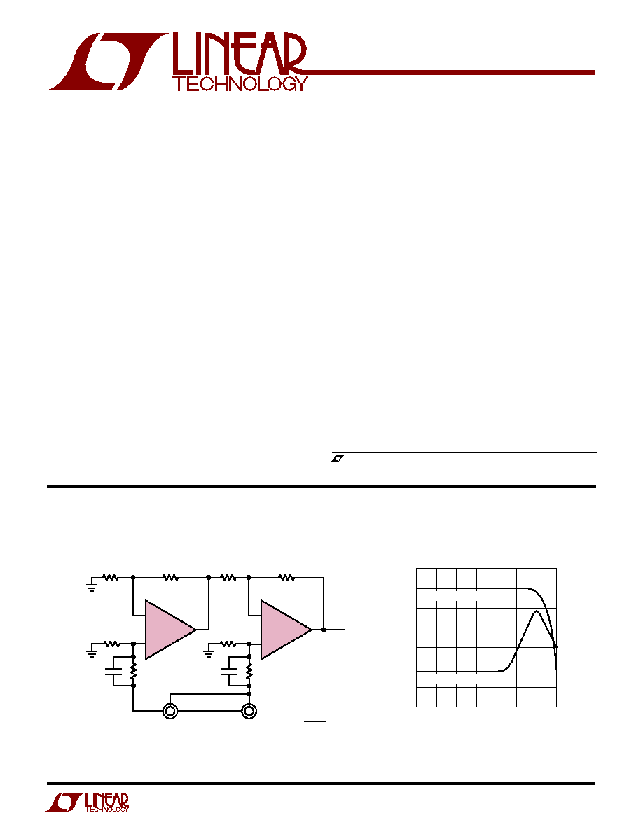
Unity-Gain Video Loop-Through Amplifier
Loop-Through Amplifier
Frequency Response
, LTC and LT are registered trademarks of Linear Technology Corporation.
+
V
OUT
1395/6/7 TA01
12.1k
0.67pF
R
F2
255
1% RESISTORS
FOR A GAIN OF G:
V
OUT
= G (V
IN+
V
IN
)
R
F1
= R
F2
R
G1
= (5G 1) R
F2
R
G2
=
TRIM CMRR WITH R
G1
HIGH INPUT RESISTANCE DOES NOT LOAD CABLE
EVEN WHEN POWER IS OFF
1/2
LT1396
R
F2
(5G 1)
R
G2
63.4
R
F1
255
R
G1
1.02k
+
1/2
LT1396
3.01k
3.01k
12.1k
V
IN
V
IN+
BNC INPUTS
0.67pF
FREQUENCY (Hz)
100
60
GAIN (dB)
50
40
30
20
10
10
1k
10k
100k
1G
1395/6/7 TA02
1M
10M 100M
0
COMMON MODE SIGNAL
NORMAL SIGNAL
2
LT1395/LT1396/LT1397
139567fb
A
U
G
W
A
W
U
W
A
R
BSOLUTE
XI
TI
S
Total Supply Voltage (V
+
to V
) ........................... 12.6V
Input Current (Note 2) .......................................
±
10mA
Output Current .................................................
±
100mA
Differential Input Voltage (Note 2) ...........................
±
5V
Output Short-Circuit Duration (Note 3) ........ Continuous
Operating Temperature Range (Note 4) . 40
°
C to 85
°
C
Specified Temperature Range (Note 5) .. 40
°
C to 85
°
C
W
U
U
PACKAGE/ORDER I FOR ATIO
ORDER
PART NUMBER
LT1397CS
T
JMAX
= 150
°
C,
JA
= 100
°
C/W
TOP VIEW
S PACKAGE
14-LEAD PLASTIC SO
1
2
3
4
5
6
7
14
13
12
11
10
9
8
OUT A
IN A
+IN A
V
+
+IN B
IN B
OUT B
OUT D
IN D
+IN D
V
+IN C
IN C
OUT C
+
+
+
+
(Note 1)
1
2
3
4
8
7
6
5
TOP VIEW
NC
V+
OUT
NC
NC
IN
+IN
V
S8 PACKAGE
8-LEAD PLASTIC SO
+
1
2
3
4
8
7
6
5
TOP VIEW
V+
OUT B
IN B
+IN B
OUT A
IN A
+IN A
V
S8 PACKAGE
8-LEAD PLASTIC SO
+
+
1
2
3
4
OUT A
IN A
+IN A
V
8
7
6
5
V+
OUT B
IN B
+IN B
TOP VIEW
MS8 PACKAGE
8-LEAD PLASTIC MSOP
+
+
1
2
3
4
5
6
7
8
TOP VIEW
GN PACKAGE
16-LEAD PLASTIC SSOP
16
15
14
13
12
11
10
9
OUT A
IN A
+IN A
V
+
+IN B
IN B
OUT B
NC
OUT D
IN D
+IN D
V
+IN C
IN C
OUT C
NC
+
+
+
+
T
JMAX
= 150
°
C,
JA
= 150
°
C/W
ORDER
PART NUMBER
LT1396CS8
T
JMAX
= 150
°
C,
JA
= 150
°
C/W
ORDER
PART NUMBER
LT1397CGN
T
JMAX
= 150
°
C,
JA
= 135
°
C/W
S8 PART MARKING
1396
GN PART MARKING
1397
ORDER
PART NUMBER
LT1396CMS8
T
JMAX
= 150
°
C,
JA
= 250
°
C/W
MS8 PART MARKING
LTDY
V
2
5 V
+
4 IN
OUT 1
TOP VIEW
S5 PACKAGE
5-LEAD PLASTIC SOT-23
+IN 3
+
ORDER
PART NUMBER
LT1395CS8
S8 PART MARKING
1395
LT1395CS6
LT1395CS5
T
JMAX
= 150
°
C,
JA
= 230
°
C/W
T
JMAX
= 150
°
C,
JA
= 250
°
C/W
ORDER
PART NUMBER
ORDER
PART NUMBER
S6 PART MARKING
S5 PART MARKING
LTMF
LTMA
OUT 1
V
2
+IN 3
6 V
+
5 EN
4 IN
TOP VIEW
S6 PACKAGE
6-LEAD PLASTIC SOT-23
+
ORDER
PART NUMBER
LT1396CDD
DD8 PART MARKING*
LABD
Consult LTC Marketing for parts specified with wider operating temperature ranges. *Temperature grades are identified by a label on the shipping container.
TOP VIEW
DD PACKAGE
8-LEAD (3mm
×
3mm) PLASTIC DFN
5
6
7
8
4
3
2
1
OUT A
IN A
+IN A
V
V
+
OUT B
IN B
+IN B
T
JMAX
= 125
°
C,
JA
= 160
°
C/W (NOTE 3)
UNDERSIDE METAL CONNECTED TO V
Storage Temperature Range ................. 65
°
C to 150
°
C
Storage Temperature Range
(DD Package) ....................................... 65
°
C to 125
°
C
Junction Temperature (Note 6) ............................ 150
°
C
Junction Temperature (DD Package) (Note 6) ..... 125
°
C
Lead Temperature (Soldering, 10 sec)................. 300
°
C
3
LT1395/LT1396/LT1397
139567fb
SYMBOL
PARAMETER
CONDITIONS
MIN
TYP
MAX
UNITS
V
OS
Input Offset Voltage
1
±
10
mV
q
±
12
mV
V
OS
/
T
Input Offset Voltage Drift
q
15
µ
V/
°
C
I
IN
+
Noninverting Input Current
10
±
25
µ
A
q
±
30
µ
A
I
IN
Inverting Input Current
10
±
50
µ
A
q
±
60
µ
A
e
n
Input Noise Voltage Density
f = 1kHz, R
F
= 1k, R
G
= 10
, R
S
= 0
4.5
nV/
Hz
+ i
n
Noninverting Input Noise Current Density
f = 1kHz
6
pA/
Hz
i
n
Inverting Input Noise Current Density
f = 1kHz
25
pA/
Hz
R
IN
Input Resistance
V
IN
=
±
3.5V
q
0.3
1
M
C
IN
Input Capacitance
2.0
pF
V
INH
Input Voltage Range, High
V
S
=
±
5V
q
3.5
4.0
V
V
S
= 5V, 0V
4.0
V
V
INL
Input Voltage Range, Low
V
S
=
±
5V
q
4.0
3.5
V
V
S
= 5V, 0V
1.0
V
V
OUTH
Output Voltage Swing, High
V
S
=
±
5V
3.9
4.2
V
V
S
=
±
5V
q
3.7
V
V
S
= 5V, 0V
4.2
V
V
OUTL
Output Voltage Swing, Low
V
S
=
±
5V
4.2
3.9
V
V
S
=
±
5V
q
3.7
V
V
S
= 5V, 0V
0.8
V
V
OUTH
Output Voltage Swing, High
V
S
=
±
5V, R
L
= 150
3.4
3.6
V
V
S
=
±
5V, R
L
= 150
q
3.2
V
V
S
= 5V, 0V; R
L
= 150
3.6
V
V
OUTL
Output Voltage Swing, Low
V
S
=
±
5V, R
L
= 150
3.6
3.4
V
V
S
=
±
5V, R
L
= 150
q
3.2
V
V
S
= 5V, 0V; R
L
= 150
0.6
V
CMRR
Common Mode Rejection Ratio
V
CM
=
±
3.5V
q
42
52
dB
I
CMRR
Inverting Input Current
V
CM
=
±
3.5V
10
16
µ
A/V
Common Mode Rejection
V
CM
=
±
3.5V
q
22
µ
A/V
PSRR
Power Supply Rejection Ratio
V
S
=
±
2V to
±
5V
q
56
70
dB
+ I
PSRR
Noninverting Input Current
V
S
=
±
2V to
±
5V
1
2
µ
A/V
Power Supply Rejection
q
3
µ
A/V
I
PSRR
Inverting Input Current
V
S
=
±
2V to
±
5V
q
2
7
µ
A/V
Power Supply Rejection
A
V
Large-Signal Voltage Gain
V
OUT
=
±
2V, R
L
= 150
50
65
dB
R
OL
Transimpedance,
V
OUT
/
I
IN
V
OUT
=
±
2V, R
L
= 150
40
100
k
I
OUT
Maximum Output Current
R
L
= 0
q
80
mA
I
S
Supply Current per Amplifier
V
OUT
= 0V
q
4.6
6.5
mA
Disable Supply Current
EN Pin Voltage = 4.5V, R
L
= 150
q
0.1
100
µ
A
(LT1395CS6 only)
I
EN
Enable Pin Current
(LT1395CS6 only)
30
110
µ
A
q
200
µ
A
SR
Slew Rate (Note 7)
A
V
= 1, R
L
= 150
500
800
V/
µ
s
ELECTRICAL C
C
HARA TERISTICS
The
q
denotes specifications which apply over the specified operating temperature range, otherwise specifications are at T
A
= 25
°
C.
For each amplifier: V
CM
= 0V, V
S
=
±
5V, EN = 0.5V, pulse tested, unless otherwise noted. (Note 5)
4
LT1395/LT1396/LT1397
139567fb
SYMBOL
PARAMETER
CONDITIONS
MIN
TYP
MAX
UNITS
ELECTRICAL C
C
HARA TERISTICS
The
q
denotes specifications which apply over the specified operating temperature range, otherwise specifications are at T
A
= 25
°
C.
For each amplifier: V
CM
= 0V, V
S
=
±
5V, pulse tested, unless otherwise noted. (Note 5)
Note 1: Absolute Maximum Ratings are those values beyond which the life
of a device may be impaired.
Note 2: This parameter is guaranteed to meet specified performance
through design and characterization. It has not been tested.
Note 3: A heat sink may be required depending on the power supply
voltage and how many amplifiers have their outputs short circuited. The
JA
specified for the DD package is with minimal PCB heat spreading
metal. Using expanded metal area on all layers of a board reduces this
value.
Note 4: The LT1395C/LT1396C/LT1397C are guaranteed functional over
the operating temperature range of 40
°
C to 85
°
C.
Note 5: The LT1395C/LT1396C/LT1397C are guaranteed to meet specified
performance from 0
°
C to 70
°
C. The LT1395C/LT1396C/LT1397C are
designed, characterized and expected to meet specified performance from
40
°
C and 85
°
C but is not tested or QA sampled at these temperatures.
For guaranteed I-grade parts, consult the factory.
Note 6: T
J
is calculated from the ambient temperature T
A
and the
power dissipation P
D
according to the following formula:
LT1395CS5: T
J
= T
A
+ (P
D
· 250
°
C/W)
LT1396CS6: T
J
= T
A
+ (P
D
· 230
°
C/W)
LT1395CS8: T
J
= T
A
+ (P
D
· 150
°
C/W)
LT1396CS8: T
J
= T
A
+ (P
D
· 150
°
C/W)
LT1396CMS8: T
J
= T
A
+ (P
D
· 250
°
C/W)
LT1396CDD: T
J
= T
A
+ (P
D
· 160
°
C/W)
LT1397CS14: T
J
= T
A
+ (P
D
· 100
°
C/W)
LT1397CGN16: T
J
= T
A
+ (P
D
· 135
°
C/W)
Note 7: Slew rate is measured at
±
2V on a
±
3V output signal.
Note 8: Differential gain and phase are measured using a Tektronix
TSG120YC/NTSC signal generator and a Tektronix 1780R Video
Measurement Set. The resolution of this equipment is 0.1% and 0.1
°
.
Ten identical amplifier stages were cascaded giving an effective
resolution of 0.01% and 0.01
°
.
Note 9: For LT1395CS6, turn-on delay time (t
ON
) is measured from
control input to appearance of 1V(50%) at the output, for V
IN
= 1V and
A
V
= 2. Likewise, turn-off delay time (t
OFF
) is measured from control
input to appearance of 1V(50%) on the output for V
IN
= 1V and
A
V
= 2. This specification is guaranteed by design and characterization.
SMALL SIGNAL
SMALL SIGNAL
SMALL SIGNAL
V
S
(V)
A
V
R
L
(
)
R
F
(
)
R
G
(
)
3dB BW (MHz)
0.1dB BW (MHz)
PEAKING (dB)
±
5
1
100
374
400
100
0.1
±
5
2
100
255
255
350
100
0.1
±
5
1
100
280
280
350
100
0.1
±
5
3
500
221
110
300
100
0.1
±
5
5
500
100
24.9
210
50
0.0
±
5
10
500
90.9
10
65
10
0.0
±
5
10
500
90.9
10
||100pF
100
50
0.1
TYPICAL AC PERFOR A CE
W U
t
ON
Turn-On Delay Time (Note 9)
R
F
= R
G
= 255
, R
L
= 100
, (LT1395CS6 only)
30
75
ns
t
OFF
Turn-Off Delay Time (Note 9)
R
F
= R
G
= 255
, R
L
= 100
, (LT1395CS6 only)
40
100
ns
3dB BW
3dB Bandwidth
A
V
= 1, R
F
= 374
, R
L
= 100
400
MHz
A
V
= 2, R
F
= R
G
= 255
, R
L
= 100
350
MHz
0.1dB BW 0.1dB Bandwidth
A
V
= 1, R
F
= 374
, R
L
= 100
100
MHz
A
V
= 2, R
F
= R
G
= 255
, R
L
= 100
100
MHz
t
r
, t
f
Small-Signal Rise and Fall Time
R
F
= R
G
= 255
, R
L
= 100
, V
OUT
= 1V
P-P
1.3
ns
t
PD
Propagation Delay
R
F
= R
G
= 255
, R
L
= 100
, V
OUT
= 1V
P-P
2.5
ns
os
Small-Signal Overshoot
R
F
= R
G
= 255
, R
L
= 100
, V
OUT
= 1V
P-P
10
%
t
S
Settling Time
0.1%, A
V
= 1, R
F
= R
G
= 280
, R
L
= 150
25
ns
dG
Differential Gain (Note 8)
R
F
= R
G
= 255
, R
L
= 150
0.02
%
dP
Differential Phase (Note 8)
R
F
= R
G
= 255
, R
L
= 150
0.04
DEG
5
LT1395/LT1396/LT1397
139567fb
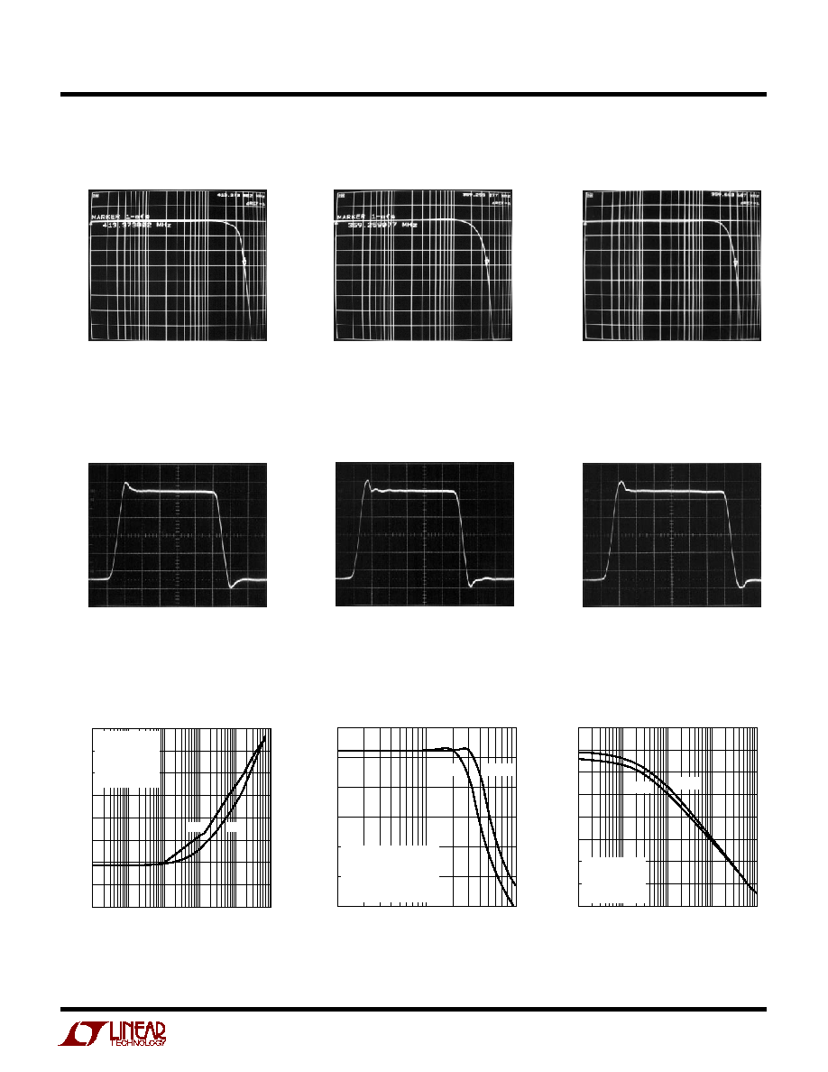
Large-Signal Transient Response
(A
V
= 1)
OUTPUT (1V/DIV)
TIME (10ns/DIV)
V
S
=
±
5V
V
IN
=
±
2.5V
R
F
= R
G
= 280
R
L
= 100
1395/6/7 G06
Large-Signal Transient Response
(A
V
= 2)
OUTPUT (1V/DIV)
TIME (10ns/DIV)
V
S
=
±
5V
V
IN
=
±
1.25V
R
F
= R
G
= 255
R
L
= 100
1395/6/7 G05
Large-Signal Transient Response
(A
V
= 1)
OUTPUT (1V/DIV)
TIME (10ns/DIV)
V
S
=
±
5V
V
IN
=
±
2.5V
R
F
= 374
R
L
= 100
1395/6/7 G04
C
C
HARA TERISTICS
U
W
A
TYPICAL PERFOR
CE
PSRR vs Frequency
Maximum Undistorted Output
Voltage vs Frequency
2nd and 3rd Harmonic Distortion
vs Frequency
FREQUENCY (Hz)
90
DISTORTION (dB)
80
60
40
30
1k
100k
1M
100M
1395/6/7 G07
100
10k
10M
50
70
110
HD2
HD3
T
A
= 25
°
C
R
F
= R
G
= 255
R
L
= 100
V
S
=
±
5V
V
OUT
= 2VPP
FREQUENCY (Hz)
1M
2
OUTPUT VOLTAGE (V
P-P
)
3
4
5
6
8
10M
100M
1395/6/7 G08
7
A
V
= +1
A
V
= +2
T
A
= 25
°
C
R
F
= 374
(A
V
= 1)
R
F
= R
G
= 255
(A
V
= 2)
R
L
= 100
V
S
=
±
5V
FREQUENCY (Hz)
20
PSRR (dB)
40
50
70
80
10k
1M
10M
100M
1395/6/7 G09
0
100k
60
30
10
+ PSRR
PSRR
T
A
= 25
°
C
R
F
= R
G
= 255
R
L
= 100
A
V
= +2
Closed-Loop Gain vs Frequency
(A
V
= 1)
0
2
4
6
GAIN (dB)
1M
10M
1G
100M
FREQUENCY (Hz)
V
S
=
±
5V
V
IN
= 10dBm
R
F
= 374
R
L
= 100
1395/6/7 G01
Closed-Loop Gain vs Frequency
(A
V
= 1)
V
S
=
±
5V
V
IN
= 10dBm
R
F
= R
G
= 280
R
L
= 100
GAIN (dB)
1M
10M
1G
100M
FREQUENCY (Hz)
Closed-Loop Gain vs Frequency
(A
V
= 2)
V
S
=
±
5V
V
IN
= 10dBm
R
F
= R
G
= 255
R
L
= 100
6
4
2
0
GAIN (dB)
1M
10M
1G
100M
FREQUENCY (Hz)
1395/6/7 G02
1395/6/7 G03
0
2
4
6