Äîêóìåíòàöèÿ è îïèñàíèÿ www.docs.chipfind.ru
1
LT1424-5
Isolated Flyback
Switching Regulator
with 5V Output
s
No Transformer "Third Winding" or Optoisolator
Required
s
Designed for Use with 1:1 Ratio Transformers
s
Fixed, Application Specific 5V Output Voltage
s
Regulation Maintained Well into Discontinuous
Mode (Light Load)
s
Load Compensation Provides Excellent
Load Regulation
s
Available in 8-Pin PDIP and SO Packages
s
Operating Frequency: 285kHz
The LT
®
1424-5 is a monolithic high power switching
regulator specifically designed for the isolated flyback
topology. No "third winding" or optoisolator is required;
the integrated circuit senses the isolated output voltage
directly from the primary side flyback waveform. A high
current, high efficiency switch is included on the die along
with all oscillator, control and protection circuitry.
The LT1424-5 operates with input supply voltages from
3V to 20V and draws only 7mA quiescent current. It can
deliver up to 400mA at 5V with no external power devices.
By utilizing current mode switching techniques, it pro-
vides excellent AC and DC line regulation.
The LT1424-5 has a number of features not found on other
switching regulator ICs. Its unique control circuitry can
maintain regulation well into discontinuous mode. Load
compensation circuitry allows for improved load regula-
tion. An externally activated shutdown mode reduces total
supply current to 20
µ
A typical for standby operation.
, LTC and LT are registered trademarks of Linear Technology Corporation.
s
Isolated Communication Supplies
s
Industrial Automation
s
Instrumentation Systems
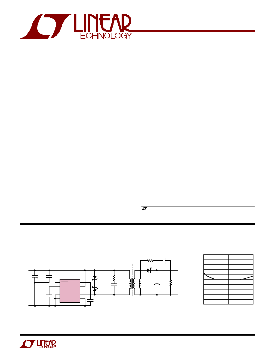
5V Output Isolated Power Supply
+
SHDN
V
C
LT1424-5
SYNC
SGND
8
1N5248
6
ISOLATION
BARRIER
T1
MBRS130LT3
7
3
1
·
·
47
47
1424-5 TA01
1.8k
MBR0540T4
7
6
5
0.1
µ
F
C1, C2: AVX TPS D107M010R0080
T1: DALE LPE-4841-A307
330pF
330pF
0.1
µ
F
C1
100
µ
F
10V
1000pF
1
5V
INPUT
COM
2
3
4
R
CCOMP
V
IN
V
SW
PGND
4
2
·
+
C2
100
µ
F
10V
5V
400mA
OUT
COM
OUTPUT CURRENT (mA)
0
OUTPUT VOLTAGE (V)
4.75
5.00
5.25
100
200
1424-5 TA02
300
400
Load Regulation
FEATURES
DESCRIPTIO
U
APPLICATIO S
U
TYPICAL APPLICATIO
U
2
LT1424-5
ABSOLUTE
M
AXI
M
U
M
RATINGS
W
W
W
U
PACKAGE/ORDER I
N
FOR
M
ATIO
N
W
U
U
Consult factory for Military grade parts.
T
JMAX
= 145
°
C,
JA
= 130
°
C/ W (N)
T
JMAX
= 145
°
C,
JA
= 110
°
C/ W (S)
1
2
3
4
8
7
6
5
TOP VIEW
S8 PACKAGE
8-LEAD PLASTIC SO
N8 PACKAGE
8-LEAD PDIP
SHDN
V
C
SYNC
SGND
R
CCOMP
V
IN
V
SW
PGND
14245
14245I
ORDER PART
NUMBER
LT1424CN8-5
LT1424CS8-5
LT1424IN8-5
LT1424IS8-5
S8 PART MARKING
ELECTRICAL CHARACTERISTICS
SYMBOL
PARAMETER
CONDITIONS
MIN
TYP
MAX
UNITS
Power Supply
V
IN(MIN)
Minimum Operating Voltage
q
2.8
3.1
V
I
CC
Supply Current
q
7.0
9.5
mA
Shutdown Mode Supply Current
q
15
40
µ
A
SHDN Pin Threshold
q
0.3
0.9
1.3
V
Feedback Amplifier
V
REF
Reference Voltage
Measured at V
SW
Pin (Note 2)
5.23
5.30
5.37
V
q
5.18
5.30
5.42
V
g
m
Feedback Amplifier Transconductance
I
C
=
±
10
µ
A (Note 3)
q
400
1000
1600
µ
mho
I
SOURCE
, I
SINK
Feedback Amplifier Source or Sink Current
q
30
50
80
µ
A
V
CL
Feedback Amplifier Clamp Voltage
1.9
V
Reference Voltage/Current Line Regulation
5V
V
IN
18V
q
0.01
0.04
%/V
Voltage Gain
(Note 4)
500
V/V
Output Switch
BV
Output Switch Breakdown Voltage
I
C
= 5mA
q
35
50
V
V(V
SW
)
Output Switch ON Voltage
I
SW
= 1A
q
0.55
0.85
V
I
LIM
Switch Current Limit
Duty Cycle = 50%, 0
°
C
T
J
125
°
C
q
1.35
1.6
1.95
A
Duty Cycle = 50%, 40
°
C
T
J
125
°
C
q
1.20
1.6
1.95
A
Duty Cycle = 80%
1.3
A
Current Amplifier
Control Pin Threshold
Duty Cycle = Minimum
0.95
1.2
1.3
V
q
0.85
1.2
1.4
V
Control Voltage to Switch Transconductance
2
A/V
(Note 1)
Supply Voltage (V
IN
) ................................................ 20V
Switch Voltage (V
SW
) .............................................. 35V
SHDN, SYNC Pin Voltage ........................................... 7V
Operating Junction Temperature Range
Commercial .......................................... 0
°
C to 125
°
C
Industrial ......................................... 40
°
C to 125
°
C
Storage Temperature Range ................. 65
°
C to 150
°
C
Lead Temperature (Soldering, 10 sec).................. 300
°
C
The
q
denotes the specifications which apply over the full operating
temperature range, otherwise specifications are at T
A
= 25
°
C. V
IN
= 5V, V
SW
Open, V
C
= 1.4V, unless otherwise specified.
3
LT1424-5
ELECTRICAL CHARACTERISTICS
SYMBOL
PARAMETER
CONDITIONS
MIN
TYP
MAX
UNITS
Timing
f
Switching Frequency
260
285
300
kHz
q
240
285
320
kHz
t
ON
Minimum Switch ON Time
170
200
260
ns
t
ED
Flyback Enable Delay Time
150
ns
t
EN
Minimum Flyback Enable Time
180
ns
Maximum Switch Duty Cycle
q
85
90
%
Load Compensation
V
REF
/
I
SW
0.9
SYNC Function
Minimum SYNC Amplitude
q
1.5
2.2
V
Synchronization Range
q
330
450
kHz
SYNC Pin Input Resistance
40
k
Note 1: Absolute Maximum Ratings are those values beyond which the life
of a device may be imparied.
Note 2: V
REF
is a parameter which is measured at the V
SW
pin. It differs
from the output voltage because it accounts for output diode drop,
transformer leakage inductance, etc. Nominal output voltage is 5V in the
intended application circuit.
Note 3: Feedback amplifier transconductance is R
REF
referred.
Note 4: Voltage gain is R
REF
referred.
The
q
denotes the specifications which apply over the full operating
temperature range, otherwise specifications are at T
A
= 25
°
C. V
IN
= 5V, V
SW
Open, V
C
= 1.4V, unless otherwise specified.
4
LT1424-5
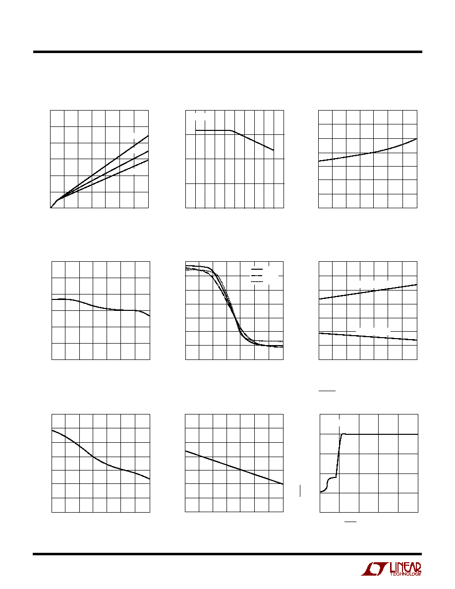
TYPICAL PERFOR A CE CHARACTERISTICS
U
W
V
C
Pin Threshold and High Clamp
Voltage vs Temperature
TEMPERATURE (
°
C)
50
REFERENCE VOLTAGE (V)
5.32
5.34
5.36
25
75
1424-5 G04
5.30
4.28
25
0
50
100
125
4.26
4.24
Reference Voltage
vs Temperature
TEMPERATURE (
°
C)
50
2.50
2.25
2.00
1.75
1.50
1.25
1.00
0.75
25
75
1424-5 G06
25
0
50
100
125
V
C
PIN VOLTAGE (V)
V
C
HIGH CLAMP
V
C
THRESHOLD
Feedback Amplifier Output
Current vs Flyback Voltage
FLYBACK VOLTAGE (V)
4.50
60
40
20
0
20
40
60
80
5.25
5.75
1424-5 G05
4.75
5.00
5.50
6.00
6.25
FEEDBACK AMPLIFIER OUTPUT CURRENT (
µ
A)
25
°
C
125
°
C
55
°
C
SHDN Pin Input Current
vs Voltage
Switching Frequency
vs Temperature
Minimum Synchronization
Voltage vs Temperature
TEMPERATURE (
°
C)
50
285
290
300
25
75
1424-5 G07
280
275
25
0
50
100
125
270
265
295
SWITCHING FREQUENCY (kHz)
TEMPERATURE (
°
C)
50
2.50
2.25
2.00
1.75
1.50
1.25
1.00
0.75
25
75
1424-5 G08
25
0
50
100
125
MINIMUM SYNCHRONIZATION VOLTAGE (V
P-P
)
SHDN PIN VOLTAGE (V)
0
1
0
1
2
3
4
4
1424-5 G09
1
2
3
5
SHDN PIN INPUT CURRENT (
µ
A)
T
A
= 25
°
C
SWITCH CURRENT (A)
0
SWITCH SATURATION VOLTAGE (V)
1.2
1.0
0.8
0.6
0.4
0.2
0
0.6
1.0
1424-5 G01
0.2
0.4
0.8
1.2
1.4
125
°
C
25
°
C
55
°
C
Switch Saturation Voltage
vs Switch Current
TEMPERATURE (
°
C)
50
3.1
3.0
2.9
2.8
2.7
2.6
2.5
2.4
25
75
1424-5 G03
25
0
50
100
125
INPUT VOLTAGE (V)
Minimum Input Voltage
vs Temperature
Switch Current Limit
vs Duty Cycle
DUTY CYCLE (%)
0
SWITCH CURRENT LIMIT (A)
40
1424-5 G02
10
20 30
50 60 70 80 90 100
2.0
1.5
1.0
0.5
0
T
A
= 25
°
C
5
LT1424-5
PGND (Pin 5): Power Ground. This pin is the emitter of the
power switch device and has large currents flowing through
it. It should be connected directly to a good quality ground
plane.
V
SW
(Pin 6): This is the collector node of the output switch
and has large currents flowing through it. Keep the traces
to the switching components as short as possible to
minimize electromagnetic radiation and voltage spikes.
V
IN
(Pin 7): Supply Voltage. Bypass input supply pin with
10
µ
F or more. The part goes into undervoltage lockout
when V
IN
drops below 2.8V. Undervoltage lockout stops
switching and pulls the V
C
pin low.
R
CCOMP
(Pin 8): Pin for the External Filter Capacitor for
Load Compensation Function. A common 0.1
µ
F
ceramic capacitor will suffice.
PI
N
FU
N
CTIO
N
S
U
U
U
SHDN (Pin 1): Shutdown. This pin is used to turn off the
regulator and reduce V
IN
input current to a few tens of
microamperes. The SHDN pin can be left floating when
unused.
V
C
(Pin 2): Control Voltage. This pin is the output of the
feedback amplifier and the input of the current compara-
tor. Frequency compensation of the overall loop is effected
by placing a capacitor between this node and ground.
SYNC (Pin 3): Pin to synchronize internal oscillator to
external frequency reference. It is directly logic compat-
ible and can be driven with any signal between 10% and
90% duty cycle. If unused, this pin should be tied to
ground.
SGND (Pin 4): Signal Ground. This pin is a clean ground.
The internal reference and feedback amplifier are referred
to it. Keep the ground path connection to the V
C
compen-
sation capacitor free of large ground currents.
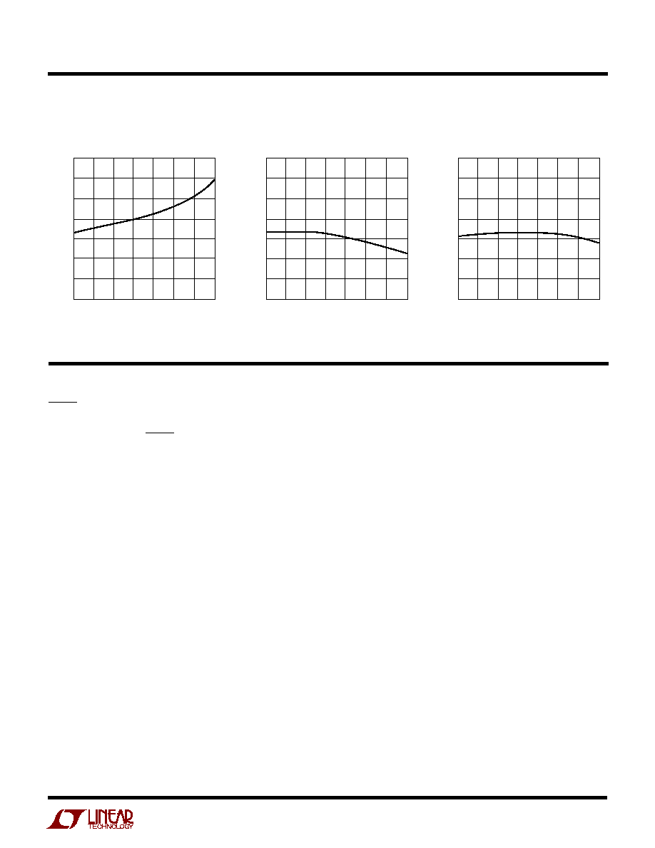
Minimum Flyback Enable Time
vs Temperature
Minimum Switch On Time
vs Temperature
Flyback Enable Delay Time
vs Temperature
TEMPERATURE (
°
C)
50
200
225
275
25
75
1424-5 G10
175
150
25
0
50
100
125
125
100
250
SWITCH ON TIME (ns)
TEMPERATURE (
°
C)
50
200
225
250
25
75
1424-5 G11
175
150
25
0
50
100
125
125
100
75
ENABLE DELAY TIME (ns)
TEMPERATURE (
°
C)
50
200
225
275
25
75
1424-5 G12
175
150
25
0
50
100
125
125
100
250
ENABLE TIME (ns)
TYPICAL PERFOR A CE CHARACTERISTICS
U
W