 | –≠–ª–µ–∫—Ç—Ä–æ–Ω–Ω—ã–π –∫–æ–º–ø–æ–Ω–µ–Ω—Ç: LT1431CN8 | –°–∫–∞—á–∞—Ç—å:  PDF PDF  ZIP ZIP |

1
LT1431
D
U
ESCRIPTIO
S
FEATURE
Programmable Reference
s
Guaranteed 0.4% Initial Voltage Tolerance
s
0.1
Typical Dynamic Output Impedance
s
Fast Turn-On
s
Sink Current Capability, 1mA to 100mA
s
Low Reference Pin Current
The LT1431 is an adjustable shunt voltage regulator with
100mA sink capability, 0.4% initial reference voltage tol-
erance, and 0.3% typical temperature stability. On-chip
divider resistors allow the LT1431 to be configured as a 5V
shunt regulator, with 1% initial voltage tolerance and
requiring no additional external components. By adding
two external resistors, the output voltage may be set to any
value between 2.5V and 36V. The nominal internal current
limit of 100mA may be decreased by including one exter-
nal resistor.
A simplified three pin version, the LT1431Z/IZ, is available
for applications as an adjustable reference and is pin
compatible with the TL431.
U
S
A
O
PPLICATI
s
Linear Regulators
s
Adjustable Power Supplies
s
Switching Power Supplies
U
A
O
PPLICATI
TYPICAL
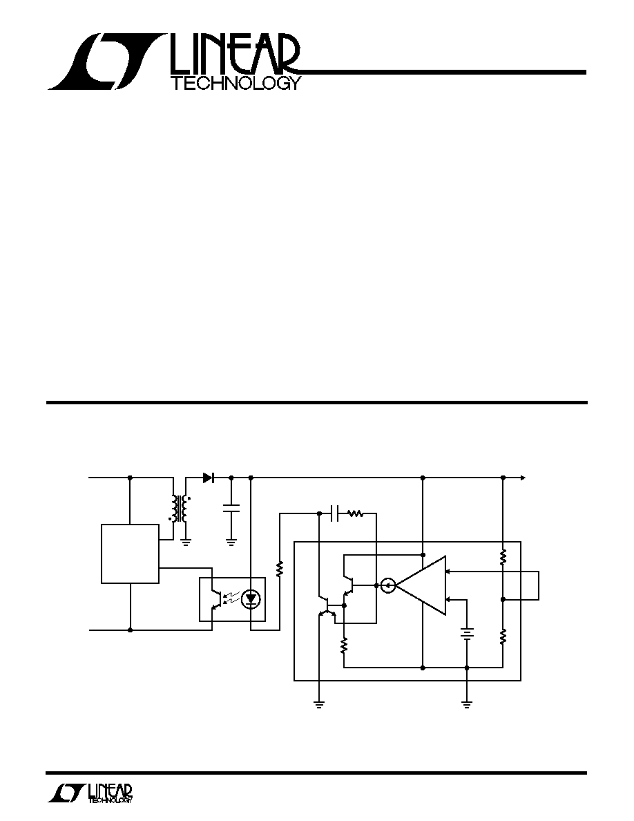
Isolated 5V Regulator
LT1431 ∑ TA01
+
+
SWITCHING
REGULATOR
≠
V
IN
COLL
COMP
V
+
LT1431
GND-F
GND-S
R
TOP
REF
R
MID
2.5V
5V
+
≠
gm =
4mA/V

2
LT1431
A
U
G
W
A
W
U
W
A
R
BSOLUTE
XI
TI
S
V+, V
COLLECTOR
....................................................... 36V
V
COMP
, R
TOP
,R
MID
,V
REF
............................................ 6V
GND-F to GND-S .................................................... 0.7V
Ambient Temperature Range
LT1431M ........................................ ≠ 55
∞
C to 125
∞
C
LT1431I ............................................ ≠ 40
∞
C to 85
∞
C
LT1431C .............................................. 0
∞
C TO 70
∞
C
JunctionTemperature Range
LT1431M ........................................ ≠ 55
∞
C to 150
∞
C
LT1431I .......................................... ≠ 40
∞
C to 100
∞
C
LT1431C ............................................. 0
∞
C to 100
∞
C
Storage Temperature Range ................ ≠65
∞
C to 150
∞
C
Lead Temperature (Soldering, 10 sec)................ 300
∞
C
LT1431CZ
LT1431IZ
ORDER PART
NUMBER
LT1431CS8
LT1431IS8
LT1431
LT1431I
ORDER PART
NUMBER
PART
MARKING
LT1431M/I
LT1431C
T
A
= 25
∞
C, I
K
= 10mA, unless otherwise specified (Note 1).
The
q
denotes specifications which apply over the operating temperature
range.
Note 1: V
KA
is the cathode voltage of the LT1431CZ/IZ and corresponds to
V
+
of the LT1431CN8/MJ8. I
K
is the cathode current of the LT1431CZ/IZ
and corresponds to I(V
+
) + I
COLLECTOR
of the LT1431CN8/MJ8/IN8.
Note 2: The LT1431 has bias current cancellation which is effective only
for V
KA
3V. A slight (
2mV) shift in reference voltage occurs when
V
KA
drops below 3V. For this reason, these tests are not performed at
V
KA
= V
REF
.
ELECTRICAL CHARACTERISTICS
LT1431MJ8
LT1431CN8
LT1431IN8
W
U
U
PACKAGE/ORDER I FOR ATIO
ORDER PART
NUMBER
1
2
3
4
8
7
6
5
TOP VIEW
COLLECTOR
COMP
V
+
R
TOP
REF
R
MID
GND-F
GND-S
N8 PACKAGE
8-LEAD PLASTIC DIP
J8 PACKAGE
8-LEAD CERAMIC DIP
T
J MAX
= 150
∞
C,
JA
= 100
∞
C/W (J)
T
J MAX
= 100
∞
C,
JA
= 130
∞
C/W (N)
1
2
3
4
8
7
6
5
TOP VIEW
REF
R
MID
GND-F
GND-S
COMP
V
+
R
TOP
S8 PACKAGE
8-LEAD PLASTIC SOIC
COLLECTOR
T
J MAX
= 100
∞
C,
JA
= 170
∞
C/W
1
2
3
BOTTOM VIEW
REF ANODE
Z PACKAGE
3-LEAD TO-92 PLASTIC
CATHODE
T
J MAX
= 100
∞
C,
JA
= 160
∞
C/W
SYMBOL
PARAMETER
CONDITIONS
MIN TYP MAX
MIN TYP MAX
UNITS
V
REF
Reference Voltage
V
KA
= 5V, I
K
= 2mA, (Note 2)
2.490 2.500 2.510
2.490 2.500 2.510
V
q
2.465
2.535
2.480
2.520
V
V
REF
/
T
Reference Drift
V
KA
= 5V, I
K
= 2mA
q
50
30
ppm/
∞
C
V
REF
/
V
KA
Voltage Ratio, Reference to
I
K
= 2mA, V
KA
= 3V to 36V
q
0.2
0.5
0.2
0.5
mV/V
Cathode (Open-Loop Gain)
|I
REF
|
Reference Input Current
V
KA
= 5V, T
A
= 25
∞
C
0.2
1.0
0.2
1.0
µ
A
q
1.5
1.2
µ
A
I
MIN
Minimum Operating Current
V
KA
= V
REF
to 36V
0.6
1.0
0.6
1.0
mA
|I
OFF
|
Off-State Cathode Current
V
KA
= 36V, V
REF
= 0V
1
1
µ
A
q
15
2
µ
A
|I
LEAK
|
Off-State Collector Leakage Current
V
COLL
= 36V, V
+
= 5V, V
REF
= 2.4V
1
1
µ
A
q
5
2
µ
A
|Z
KA
|
Dynamic Impedance
V
KA
= V
REF
, I
K
= 1mA to 100mA, f
1kHz
0.2
0.2
I
LIM
Collector Current Limit
V
KA
= V
REF
+ 50mV
q
80
360
100
260
mA
5V Reference Output
Internal Divider Used, I
K
= 2mA
4.950 5.000 5.050
4.950 5.000 5.050
V

3
LT1431
C
C
HARA TERISTICS
U
W
A
TYPICAL PERFOR
CE
V
KA
(V)
0
I
K
(
µ
A)
600
800
1000
4.0
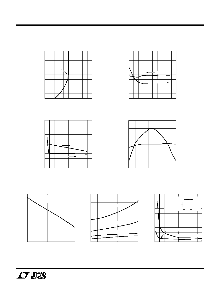
LT1431 ∑ TPC01
400
200
0
1.0
2.0
3.0
5.0
I
MIN
500
700
900
300
100
0.5
4.5
1.5
2.5
3.5
2.5V Reference I
K
vs V
KA
V
+
(V)
2.5
V
REF
(V)
2.501
2.503
2.505
3.3
LT1431 ∑ TPC02
2.499
2.497
2.495
2.7
2.9
3.1
3.5
I
REF
(
µ
A)
1.5
2.5
3.5
0.5
≠0.5
≠1.5
V
REF
I
REF
2.500
2.502
2.504
2.498
2.496
3.2
2.6
2.8
3.0
3.4
1.0
2.0
3.0
0
≠1.0
V
REF
and I
REF
vs V
+
V
+
(V)
0
V
REF
(V)
2.501
2.503
2.505
32
LT1431 ∑ TPC03
2.499
2.497
2.495
8
16
24
40
I
REF
(
µ
A)
1.5
2.5
3.5
0.5
≠0.5
≠1.5
V
REF
I
REF
2.500
2.502
2.504
2.498
2.496
28
4
12
20
36
1.0
2.0
3.0
0
≠1.0
V
REF
and I
REF
vs V
+
Propagation Delay vs Overdrive
I
LIMIT
vs Temperature with
External Resistor
COLLECTOR V
SAT
vs
Temperature vs Current
V
REF
and I
REF
vs Temperature
TEMPERATURE (∞C)
≠50
V
REF
(V)
2.4975
2.5000
2.5025
25
75
LT1027 ∑ TPC04
2.4950
2.4925
≠25
0
50
100
125
2.4900
2.4875
0.33
0.66
1.00
0
≠0.33
≠0.66
≠1.00
I
REF
(
µ
A)
V
REF
I
REF
TEMPERATURE (∞C)
≠50
I
LIMIT
(NORMALIZED)
1.000
1.125
1.250
25
75
LT1431 ∑ TPC05
0.875
0.750
≠25
0
50
100
125
0.625
0.500
I
LIMIT
=
0.7
R
LIM
+ 3.6
AT 25∞C
TEMPERATURE (∞C)
≠50
V
SAT
(V)
0.80
1.00
1.20
25
75
LT1431 ∑ TPC06
0.60
0.40
≠25
0
50
100
125
0.20
0
I
COLL
= 100mA
I
COLL
= 20mA
I
COLL
= 10mA
I
COLL
= 50mA
OVERDRIVE (mV)
0
PROPAGATION DELAY (
µ
s)
90
120
150
200
LT1431 ∑ TPC07
60
30
0
50
100
150
250
75
105
135
45
15
3
1
1k
OUTPUT
5
6
5V
LT1431
V
REF
± OVERDRIVE
OUTPUT HIGH-TO-LOW
OUTPUT LOW-TO-HIGH

4
LT1431
C
C
HARA TERISTICS
U
W
A
TYPICAL PERFOR
CE
FREQUENCY (Hz)
20
REF-TO-COLL 1k LOAD A
V
(dB)
40
80
120
140
100
10k
100k
10M
LT1431 ∑ TPC08
0
1k
1M
100
60
≠20
≠90
≠45
45
135
180
≠135
90
0
≠180
PHASE (DEG)
PHASE
A
V
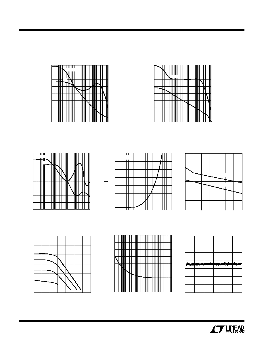
Voltage Gain and Phase
vs Frequency
FREQUENCY (Hz)
10
10
100
10k
100k
10M
LT1431 ∑ TPC09
1k
1M
≠90
≠45
45
135
180
≠135
90
0
≠180
PHASE (DEG)
10
9
10
8
10
7
10
6
10
5
10
4
10
3
10
2
REF-TO-COLL gm (m )
PHASE
gm
Transconductance and Phase
vs Frequency (REF to COLL)
Transconductance and Phase vs
Frequency (Ref to Comp)
Dynamic Impedance vs Frequency
TEMPERATURE (∞C)
≠50
V
COMP
(V)
2.0
2.5
3.0
25
75
LT1431 ∑ TPC12
1.5
1.0
≠25
0
50
100
125
0.5
0
I
COLL
= 100mA
I
COLL
= 10mA
V
COMP
vs Temperature vs I
COLL
I
COMP
vs V
COMP
vs V
REF
Noise vs Frequency
0.1Hz to 10Hz Noise
FREQUENCY (Hz)
NOISE (nV/
Hz)
1000
1
100
1k
100k
LT1431 ∑ G14
10
10k
500
0
TIME (MINUTES)
0
3
5
LT1431 ∑ TPC15
1
2
4
6
NOISE VOLTAGE (50
µ
V/DIV)
FREQUENCY (Hz)
10
4
100
10k
100k
10M
LT1431 ∑ TPC10
1k
1M
≠100
≠80
≠40
0
20
≠120
≠20
≠60
≠140
PHASE (DEG)
3
◊
10
3
10
3
0.1
REF-TO-COLL gm (
µ
)
PHASE
gm
3
◊
10
2
FREQUENCY (Hz)
100
0.8
1.0
1.2
1.4
1k
10k
100k
LT1431 ∑ TPC11
0.6
0.4
0.2
0
I
K
100mA
Z
KA
(
)
V
COMP
(V)
0
I
COMP
(
µ
A)
400
500
600
1.5
2.5
LT1431 ∑ TPC13
300
200
0.5
1.0
2.0
3.0
3.5
100
0
V
REF
= 5V
V
REF
= 4V
V
REF
= 3V
V
REF
= 2.53V

5
LT1431
PI FU CTIO S
U
U
U
COLL (Pin 1): Open collector of the output transistor. The
maximum pin voltage is 26V. The saturation voltage at
100mA is approximately 1V.
COMP (Pin 2): Base of the driver for the output transistor.
This pin allows additional compensation for complex
feedback systems and shutdown of the regulator. It must
be left open if unused.
V
+
(Pin 3): Bias voltage for the entire shunt regulator. The
maximum input voltage is 36V and the minimum to
operate is equal to V
REF
(2.5V). The quiescent current is
typically 0.6mA.
R
TOP
(Pin 4): Top of the on-chip 5k-5k resistive divider
that guarantees 1% accuracy of operation as a 5V shunt
regulator with no external trim. The pin is tied to COLL for
self-contained 5V operation. It may be left open if unused.
See note on parasitic diodes below.
GND-S (Pin 5): Ground reference for the on-chip resistive
divider and shunt regulator circuitry except for the output
transistor. This pin allows external current limit of the
output transistor with one resistor between GND-F (force)
and GND-S (sense).
GND-F (Pin 6): Emitter of the output transistor and sub-
strate connection for the die.
R
MID
(Pin 7): Middle of the on-chip resistive divider string
between R
TOP
and GND-S. The pin is tied to REF for self-
contained 5V operation. It may be left open if unused.
REF (Pin 8): Control pin of the shunt regulator with a 2.5V
threshold. If V
+
> 3V, input bias current cancellation
reduces I
B
to 0.2
µ
A typical.
COMP, R
TOP
, R
MID
, and REF have static discharge protec-
tion circuits that must not be activated on a continuous
basis. Therefore, the absolute maximum DC voltage on
these pins is 6V, well beyond the normal operating condi-
tions.
As with all bipolar ICs, the LT1431 contains parasitic
diodes which must not be forward biased or else anoma-
lous behavior will result. Pin conditions to be avoided are
R
TOP
below R
MID
in voltage and any pin below GND-F in
voltage (except for GND-S).
The following pin definitions apply to the Z package.
CATHODE (Pin 1): Corresponds to COLL and V
+
tied
together.
ANODE (Pin 2): Corresponds to GND-S and GND-F tied
together.
REF (Pin 3): Corresponds to REF.
W
I
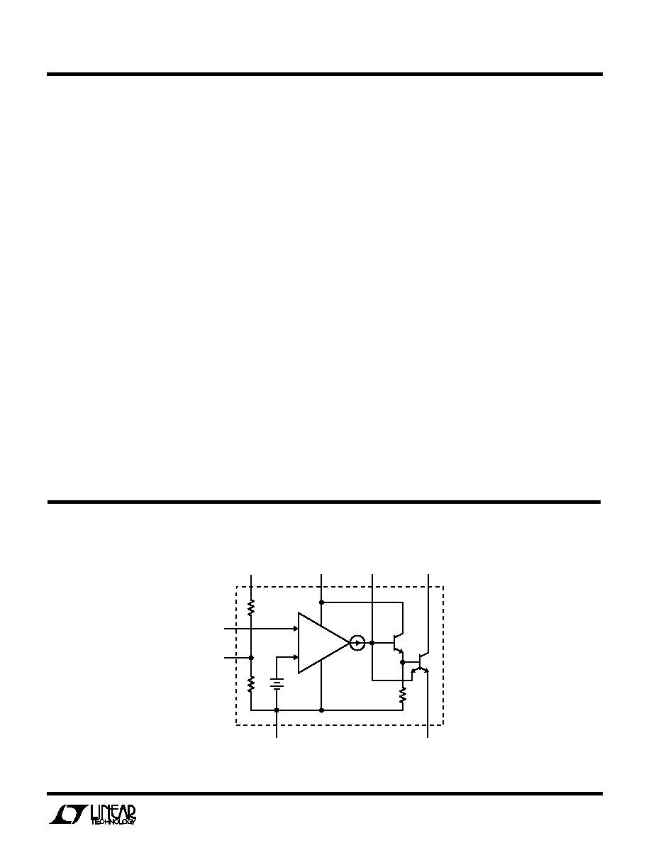
D AGRA
BLOCK
LT1431 ∑ BD01
COMP
V
+
GND-FORCE
GND-SENSE
R
TOP
REF
R
MID
2.5V
+
≠
gm =
4mA/V
5k
COLLECTOR
8
7
5
4
3
2
1
6
5k
