14901afa.pm6

1
LT1490A/LT1491A
14901afa
Dual/Quad Over-The-Top
Micropower Rail-to-Rail
Input and Output Op Amps
s
Low Input Offset Voltage: 500
µ
V Max
s
Output Swings to 10mV Max from V
s
Rail-to-Rail Input and Output
s
Micropower: 50
µµ
µµ
µ
A/Amplifier Max
s
Tiny 3mm
××
××
×
3mm
××
××
×
0.8mm DFN Package
s
Over-The-Top
®
Input Common Mode Range Extends
44V Above V
, Independent of V
+
s
Specified on 3V, 5V and
±
15V Supplies
s
High Output Current: 20mA
s
Output Drives 10,000pF with Output Compensation
s
Reverse Battery Protection to 18V
s
No Supply Sequencing Problems
s
High Voltage Gain: 1500V/mV
s
High CMRR: 98dB
s
No Phase Reversal
s
Gain Bandwidth Product: 200kHz
The LT
®
1490A/LT1491A are dual and quad op amps with a
low input offset voltage of 500
µ
V max. The LT1490A/LT1491A
operate on all single and split supplies with a total voltage of
2V to 44V, drawing only 40
µ
A of quiescent current per
amplifier. These amplifiers are reverse supply protected; they
draw virtually no current for reverse supply up to 18V. The
input range of the LT1490A/LT1491A includes both supplies
and the output swings to both supplies. Unlike most mi-
cropower op amps, the LT1490A/LT1491A can drive heavy
loads; their rail-to-rail outputs drive 20mA. The LT1490A/
LT1491A are unity-gain stable and drive all capacitive loads
up to 10,000pF when optional 0.22
µ
F and 150
compensa-
tion is used.
The LT1490A/LT1491A have a unique input stage that oper-
ates and remains high impedance when above the positive
supply. The inputs take 44V both differential and common
mode even when operating on a 3V supply. Built-in resis-
tors protect the inputs for faults below the negative supply
up to 15V. There is no phase reversal of the output for inputs
15V below V
or 44V above V
, independent of V
+
.
The LT1490A dual op amp is available in the 8-pin MSOP,
PDIP and SO packages. For space limited applications
LT1490A is available in a 3mm
×
3mm
×
0.8mm, dual fine
pitch leadless package (DFN). The quad LT1491A is avail-
able in the 14-pin SO and PDIP packages.
s
Battery- or Solar-Powered Systems
Portable Instrumentation
Sensor Conditioning
s
Supply Current Sensing
s
Battery Monitoring
s
Micropower Active Filters
s
4mA to 20mA Transmitters
Battery Monitor
+
+
RA
2k
Q2
2N3904
S1
S1 = OPEN, GAIN = 1
S1 = CLOSED, GAIN = 10
R
A
= R
B
V
S
= 5V, 0V
10k
90.9k
V
OUT
LOGIC
1490A TA01
LOGIC HIGH (5V) = CHARGING
LOGIC LOW (0V) = DISCHARGING
R
G
10k
Q1
2N3904
R
S
0.2
CHARGER
VOLTAGE
1/4 LT1491A
1/4 LT1491A
R
A
´
2k
R
B
2k
V
BATT
= 12V
I
BATT
+
R
B
´
2k
LOAD
+
+
V
OUT
(R
S
)(R
G
/R
A
)(GAIN)
V
OUT
GAIN
I
BATT
= = AMPS
1/4 LT1491A
1/4 LT1491A
, LTC and LT are registered trademarks of Linear Technology Corporation.
Over-The-Top is a registered trademark of Linear Technology Corporation.
DESCRIPTIO
U
FEATURES
APPLICATIO S
U
TYPICAL APPLICATIO
U

2
LT1490A/LT1491A
14901afa
Total Supply Voltage (V
+
to V
) ............................. 44V
Differential Input Voltage ........................................ 44V
Input Current .....................................................
±
12mA
Output Short-Circuit Duration (Note 2) ........ Continuous
Operating Temperature Range (Note 3)
LT1490AC/LT1491AC ......................... 40
°
C to 85
°
C
LT1490AI/LT1491AI ........................... 40
°
C to 85
°
C
LT1490AH/LT1491AH ...................... 40
°
C to 125
°
C
*Temperature grades are identified by a label on the shipping container.
Consult LTC Marketing for parts specified with wider operating temperature ranges.
LT1490ACN8
LT1490ACS8
LT1490AIN8
LT1490AIS8
LT1490AHS8
T
JMAX
= 150
°
C,
JA
= 250
°
C/ W
S8
PART MARKING
MS8
PART MARKING
ORDER PART
NUMBER
LTNG
LTPU
LTRK
1490A
1490AI
1490AH
LT1490ACMS8
LT1490AIMS8
LT1490AHMS8
Specified Temperature Range (Note 4)
LT1490AC/LT1490AI .......................... 40
°
C to 85
°
C
LT1491AC/LT1491AI .......................... 40
°
C to 85
°
C
LT1490AH/LT1491AH ...................... 40
°
C to 125
°
C
Junction Temperature .......................................... 150
°
C
Junction Temperature (DD Package) ................... 125
°
C
Storage Temperature Range ................ 65
°
C to 150
°
C
Storage Temperature Range
DD Package ..................................... 65
°
C to 125
°
C
Lead Temperature (Soldering, 10 sec)................. 300
°
C
T
JMAX
= 150
°
C,
JA
= 130
°
C/ W (N8)
T
JMAX
= 150
°
C,
JA
= 190
°
C/ W (S8)
1
2
3
4
8
7
6
5
TOP VIEW
N8 PACKAGE
8-LEAD PDIP
S8 PACKAGE
8-LEAD PLASTIC SO
V
+
OUT B
IN B
+IN B
A
B
OUT A
IN A
+IN A
V
ORDER PART
NUMBER
1
2
3
4
OUT A
IN A
+IN A
V
8
7
6
5
V
+
OUT B
IN B
+IN B
TOP VIEW
MS8 PACKAGE
8-LEAD PLASTIC MSOP
A
B
(Note 1)
ABSOLUTE AXI U RATI GS
W
W
W
U
PACKAGE/ORDER I FOR ATIO
U
U
W
TOP VIEW
S PACKAGE
14-LEAD PLASTIC SO
N PACKAGE
14-LEAD PDIP
1
2
3
4
5
6
7
14
13
12
11
10
9
8
OUT A
IN A
+IN A
V
+
+IN B
IN B
OUT B
OUT D
IN D
+IN D
V
+IN C
IN C
OUT C
A
D
B
C
T
JMAX
= 150
°
C,
JA
= 110
°
C/ W (N)
T
JMAX
= 150
°
C,
JA
= 150
°
C/ W (S)
LT1491ACN
LT1491ACS
LT1491AIN
LT1491AIS
LT1491AHS
ORDER PART
NUMBER
TOP VIEW
DD PACKAGE
8-LEAD (3mm
×
3mm) PLASTIC DFN
5
6
7
8
4
3
2
1
OUT A
IN A
+IN A
V
V
+
OUT B
IN B
+IN B
A
B
ORDER PART
NUMBER
T
JMAX
= 125
°
C,
JA
= 160
°
C/ W (NOTE 2)
UNDERSIDE METAL CONNECTED TO V
LT1490ACDD
LT1490AIDD
DD
PART MARKING*
LAAH
3
LT1490A/LT1491A
14901afa
LT1490AC/LT1491AC
LT1490AI/LT1491AI
SYMBOL
PARAMETER
CONDITIONS
MIN
TYP
MAX
UNITS
V
OS
Input Offset Voltage (Note 5)
LT1490A N, S Packages
110
500
µ
V
0
°
C
T
A
70
°
C
q
700
µ
V
40
°
C
T
A
85
°
C
q
800
µ
V
LT1490A MS8 Package, LT1491A N, S Packages
220
1000
µ
V
0
°
C
T
A
70
°
C
q
1200
µ
V
40
°
C
T
A
85
°
C
q
1400
µ
V
LT1490A DD Package
250
1200
µ
V
0
°
C
T
A
70
°
C
q
1400
µ
V
40
°
C
T
A
85
°
C
q
1600
µ
V
Input Offset Voltage Drift (Note 9)
40
°
C
T
A
85
°
C
q
2
4
µ
V/
°
C
LT1490A DD Package, 40
°
C
T
A
85
°
C
q
2
6
µ
V/
°
C
I
OS
Input Offset Current
q
0.2
0.8
nA
V
CM
= 44V (Note 6)
q
0.8
µ
A
I
B
Input Bias Current
q
1
8
nA
V
CM
= 44V (Note 6)
q
3
10
µ
A
V
S
= 0V
0.3
nA
Input Bias Current Drift
40
°
C
T
A
85
°
C
q
2
pA/
°
C
Input Noise Voltage
0.1Hz to 10Hz
1
µ
V
P-P
e
n
Input Noise Voltage Density
f = 1kHz
50
nV/
Hz
i
n
Input Noise Current Density
f = 1kHz
0.015
pA/
Hz
R
IN
Input Resistance
Differential
6
17
M
Common Mode, V
CM
= 0V to 44V
4
11
M
C
IN
Input Capacitance
4.6
pF
Input Voltage Range
q
0
44
V
CMRR
Common Mode Rejection Ratio
V
CM
= 0V to V
CC
1V
q
84
98
dB
(Note 6)
V
CM
= 0V to 44V
q
80
98
dB
A
VOL
Large-Signal Voltage Gain
V
S
= 3V, V
O
= 500mV to 2.5V, R
L
= 10k
200
1500
V/mV
0
°
C
T
A
70
°
C
q
133
V/mV
40
°
C
T
A
85
°
C
q
100
V/mV
V
S
= 5V, V
O
= 500mV to 4.5V, R
L
= 10k
400
1500
V/mV
0
°
C
T
A
70
°
C
q
250
V/mV
40
°
C
T
A
85
°
C
q
200
V/mV
V
OL
Output Voltage Swing Low
V
S
= 3V, No Load
q
3
10
mV
V
S
= 3V, I
SINK
= 5mA
q
250
450
mV
V
S
= 5V, No Load
q
3
10
mV
V
S
= 5V, I
SINK
= 5mA
q
250
500
mV
V
S
= 5V, I
SINK
= 10mA
330
500
mV
V
OH
Output Voltage Swing High
V
S
= 3V, No Load
q
2.95
2.978
V
V
S
= 3V, I
SOURCE
= 5mA
q
2.55
2.6
V
V
S
= 5V, No Load
q
4.95
4.978
V
V
S
= 5V, I
SOURCE
= 10mA
q
4.30
4.6
V
I
SC
Short-Circuit Current (Note 2)
V
S
= 3V, Short to GND
10
15
mA
V
S
= 3V, Short to V
CC
10
30
mA
V
S
= 5V, Short to GND
15
25
mA
V
S
= 5V, Short to V
CC
15
30
mA
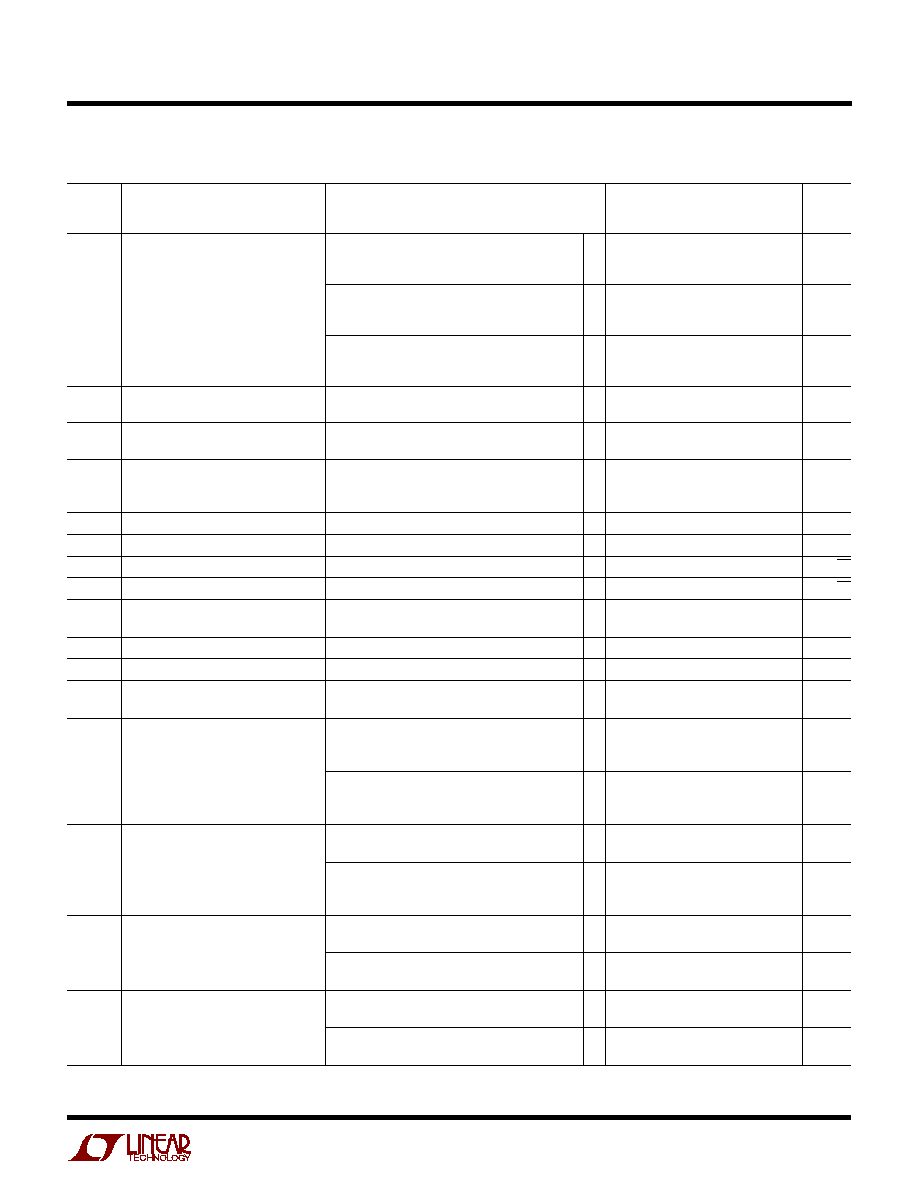
ELECTRICAL CHARACTERISTICS
The
q
denotes specifications which apply over the full operating temperature
range of 40
°
C
T
A
85
°
C, otherwise specifications are at T
A
= 25
°
C. V
S
= 3V, 0V; V
S
= 5V, 0V; V
CM
= V
OUT
= half supply unless
otherwise noted. (Note 4)

4
LT1490A/LT1491A
14901afa
LT1490AC/LT1491AC
LT1490AI/LT1491AI
SYMBOL
PARAMETER
CONDITIONS
MIN
TYP
MAX
UNITS
PSRR
Power Supply Rejection Ratio
V
S
= 2.5V to 12.5V, V
CM
= V
O
= 1V
q
84
98
dB
Minimum Operating Supply Voltage
q
2
2.5
V
Reverse Supply Voltage
I
S
= 100
µ
A per Amplifier
q
18
27
V
I
S
Supply Current per Amplifier
40
50
µ
A
(Note 7)
q
55
µ
A
GBW
Gain Bandwidth Product
f = 1kHz
110
180
kHz
(Note 6)
0
°
C
T
A
70
°
C
q
100
kHz
40
°
C
T
A
85
°
C
q
90
kHz
SR
Slew Rate
A
V
= 1, R
L
=
0.035
0.06
V/
µ
s
(Note 8)
0
°
C
T
A
70
°
C
q
0.031
V/
µ
s
40
°
C
T
A
85
°
C
q
0.030
V/
µ
s
ELECTRICAL CHARACTERISTICS
The
q
denotes specifications which apply over the full operating temperature
range of 40
°
C
T
A
85
°
C, otherwise specifications are at T
A
= 25
°
C. V
S
= 3V, 0V; V
S
= 5V, 0V; V
CM
= V
OUT
= half supply unless
otherwise noted. (Note 4)
LT1490AC/LT1491AC
LT1490AI/LT1491AI
SYMBOL
PARAMETER
CONDITIONS
MIN
TYP
MAX
UNITS
V
OS
Input Offset Voltage (Note 5)
LT1490A N, S Packages
150
700
µ
V
0
°
C
T
A
70
°
C
q
950
µ
V
40
°
C
T
A
85
°
C
q
1100
µ
V
LT1490A MS8 Package, LT1491A N, S Packages
250
1200
µ
V
0
°
C
T
A
70
°
C
q
1350
µ
V
40
°
C
T
A
85
°
C
q
1500
µ
V
LT1490A DD Package
285
1400
µ
V
0
°
C
T
A
70
°
C
q
1550
µ
V
40
°
C
T
A
85
°
C
q
1700
µ
V
Input Offset Voltage Drift (Note 9)
40
°
C
T
A
85
°
C
q
2
6
µ
V/
°
C
LT1490A DD Package, 40
°
C
T
A
85
°
C
q
2
7
µ
V/
°
C
I
OS
Input Offset Current
q
0.2
0.8
nA
I
B
Input Bias Current
q
1
8
nA
Input Bias Current Drift
40
°
C
T
A
85
°
C
q
5
pA/
°
C
Input Noise Voltage
0.1Hz to 10Hz
1
µ
V
P-P
e
n
Input Noise Voltage Density
f = 1kHz
50
nV/
Hz
i
n
Input Noise Current Density
f = 1kHz
0.015
pA/
Hz
R
IN
Input Resistance
Differential
6
17
M
Common Mode, V
CM
= 15V to 14V
15000
M
C
IN
Input Capacitance
4.6
pF
Input Voltage Range
q
15
29
V
CMRR
Common Mode Rejection Ratio
V
CM
= 15V to 29V
q
80
98
dB
A
VOL
Large-Signal Voltage Gain
V
O
=
±
14V, R
L
= 10k
100
250
V/mV
0
°
C
T
A
70
°
C
q
75
V/mV
40
°
C
T
A
85
°
C
q
50
V/mV
V
O
Output Voltage Swing
No Load
q
±
14.9
±
14.978
V
I
OUT
=
±
5mA
q
±
14.5
±
14.750
V
I
OUT
=
±
10mA
±
14.5
±
14.670
V
The
q
denotes specifications which apply over the full operating temperature range of 40
°
C
T
A
85
°
C, otherwise specifications are
at T
A
= 25
°
C. V
S
=
±
15V; V
CM
= 0V, V
OUT
= 0V unless otherwise noted. (Note 4)

5
LT1490A/LT1491A
14901afa
LT1490AH/LT1491AH
SYMBOL
PARAMETER
CONDITIONS
MIN
TYP
MAX
UNITS
V
OS
Input Offset Voltage (Note 5)
LT1490AHS8
110
500
µ
V
q
2500
µ
V
LT1490AHMS8, LT1491AHS
220
1000
µ
V
q
3000
µ
V
Input Offset Voltage Drift (Note 9)
q
3
6
µ
V/
°
C
I
OS
Input Offset Current
q
2
nA
V
CM
= 44V (Note 6)
q
1.5
µ
A
I
B
Input Bias Current
q
20
nA
V
CM
= 44V (Note 6)
q
15
µ
A
Input Voltage Range
q
0.3
44
V
CMRR
Common Mode Rejection Ratio
V
CM
= 0.3V to V
CC
1V
q
60
dB
(Note 6)
V
CM
= 0.3V to 44V
q
74
dB
A
VOL
Large-Signal Voltage Gain
V
S
= 3V, V
O
= 500mV to 2.5V, R
L
= 10k
200
1500
V/mV
q
25
V/MV
V
S
= 5V, V
O
= 500mV to 4.5V, R
L
= 10k
400
1500
V/mV
q
50
V/mV
V
OL
Output Voltage Swing Low
V
S
= 3V, No Load
q
15
mV
V
S
= 3V, I
SINK
= 2.5mA
q
450
mV
V
S
= 5V, No Load
q
15
mV
V
S
= 5V, I
SINK
= 2.5mA
q
500
mV
V
OH
Output Voltage Swing High
V
S
= 3V, No Load
q
2.925
V
V
S
= 3V, I
SOURCE
= 5mA
q
2.350
V
V
S
= 5V, No Load
q
4.925
V
V
S
= 5V, I
SOURCE
= 10mA
q
4.100
V
PSRR
Power Supply Rejection Ratio
V
S
= 2.5V to 12.5V, V
CM
= V
O
= 1V
q
80
dB
Minimum Operating Supply Voltage
q
2.5
V
Reverse Supply Voltage
I
S
= 100
µ
A per Amplifier
q
18
V
The
q
denotes specifications which apply over the full operating temperature range of 40
°
C
T
A
125
°
C. V
S
= 3V, 0V; V
S
= 5V, 0V;
V
CM
= V
OUT
= half supply unless otherwise noted. (Note 4)
LT1490AC/LT1491AC
LT1490AI/LT1491AI
SYMBOL
PARAMETER
CONDITIONS
MIN
TYP
MAX
UNITS
I
SC
Short-Circuit Current (Note 2)
Short to GND
±
20
±
25
mA
0
°
C
T
A
70
°
C
q
±
15
mA
40
°
C
T
A
85
°
C
q
±
10
mA
PSRR
Power Supply Rejection Ratio
V
S
=
±
1.25V to
±
22V
q
88
98
dB
I
S
Supply Current per Amplifier
50
70
µ
A
q
85
µ
A
GBW
Gain Bandwidth Product
f = 1kHz
125
200
kHz
0
°
C
T
A
70
°
C
q
110
kHz
40
°
C
T
A
85
°
C
q
100
kHz
SR
Slew Rate
A
V
= 1, R
L
=
,
V
O
=
±
10V,
0.0375
0.07
V/
µ
s
Measure at V
O
=
±
5V
0
°
C
T
A
70
°
C
q
0.0330
V/
µ
s
40
°
C
T
A
85
°
C
q
0.0300
V/
µ
s
ELECTRICAL CHARACTERISTICS
The
q
denotes specifications which apply over the full operating temperature
range of 40
°
C
T
A
85
°
C, otherwise specifications are at T
A
= 25
°
C. V
S
=
±
15V; V
CM
= 0V, V
OUT
= 0V unless otherwise noted. (Note 4)