 | –≠–ª–µ–∫—Ç—Ä–æ–Ω–Ω—ã–π –∫–æ–º–ø–æ–Ω–µ–Ω—Ç: LT1491IS | –°–∫–∞—á–∞—Ç—å:  PDF PDF  ZIP ZIP |
1
LT1490/LT1491
Dual and Quad
Micropower Rail-to-Rail
Input and Output Op Amps
s
Rail-to-Rail Input and Output
s
Single Supply Input Range: ≠ 0.4V to 44V
s
Micropower: 50
µµ
µµ
µ
A/Amplifier Max
s
MSOP Package
s
Specified on 3V, 5V and
±
15V Supplies
s
High Output Current: 20mA
s
Output Drives 10,000pF with Output Compensation
s
Reverse Battery Protection to 18V
s
No Supply Sequencing Problems
s
High Voltage Gain: 1500V/mV
s
High CMRR: 98dB
s
No Phase Reversal
s
Gain Bandwidth Product: 200kHz
The dual LT
Æ
1490 and quad LT1491 op amps operate on all
single and split supplies with a total voltage of 2V to 44V
drawing only 40
µ
A of quiescent current per amplifier. These
amplifiers are reverse supply protected; they draw no current
for reverse supply up to 18V. The input range of the LT1490/
LT1491 includes both supplies and the output swings to both
supplies. Unlike most micropower op amps, the LT1490/
LT1491 can drive heavy loads; their rail-to-rail outputs drive
20mA. The LT1490/LT1491 are unity-gain stable and drive all
capacitive loads up to 10,000pF when optional 0.22
µ
F and
150
compensation is used.
The LT1490/LT1491 have a unique input stage that oper-
ates and remains high impedance when above the positive
supply. The inputs take 44V both differential and common
mode even when operating on a 3V supply. Built-in resis-
tors protect the inputs for faults below the negative supply
up to 22V. There is no phase reversal of the output for inputs
22V below V
≠
or 44V above V
≠
, independent of V
+
.
The LT1490 dual op amp is available in the 8-pin MSOP,
SO and PDIP packages. The quad LT1491 is available in
the 14-pin SO and PDIP packages.
For new designs it is recommended that the LT1490A/
LT1491A be used instead of the LT1490/LT1491. See the
LT1490A/LT1491A data sheet for details.
s
Battery- or Solar-Powered Systems
Portable Instrumentation
Sensor Conditioning
s
Supply Current Sensing
s
Battery Monitoring
s
Micropower Active Filters
s
4mA to 20mA Transmitters
≠
+
≠
+
RA
2k
Q2
2N3904
S1
S1 = OPEN, GAIN = 1
S1 = CLOSED, GAIN = 10
R
A
= R
B
V
S
= 5V, 0V
10k
90.9k
V
OUT
LOGIC
1490/91 TA01
LOGIC HIGH (5V) = CHARGING
LOGIC LOW (0V) = DISCHARGING
R
G
10k
Q1
2N3904
R
S
0.2
CHARGER
VOLTAGE
A
1/4 LT1491
B
1/4 LT1491
R
A
'
2k
R
B
2k
V
BATT
= 12V
I
BATT
+
R
B
'
2k
LOAD
≠
+
≠
+
C
1/4 LT1491
D
1/4 LT1491
V
OUT
(R
S
)(R
G
/R
A
)(GAIN)
V
OUT
GAIN
I
BATT
= = AMPS
Battery Monitor
FEATURES
DESCRIPTIO
U
APPLICATIO S
U
TYPICAL APPLICATIO
U
, LTC and LT are registered trademarks of Linear Technology Corporation.
2
LT1490/LT1491
Junction Temperature ........................................... 150
∞
C
Specified Temperature Range (Note 3) .. ≠ 40
∞
C to 85
∞
C
Storage Temperature Range ................. ≠ 65
∞
C to 150
∞
C
Lead Temperature (Soldering, 10 sec).................. 300
∞
C
Total Supply Voltage (V
+
to V
≠
) .............................. 44V
Input Differential Voltage ......................................... 44V
Input Current ......................................................
±
25mA
Output Short-Circuit Duration (Note 2) .........Continuous
Operating Temperature Range ................ ≠ 40
∞
C to 85
∞
C
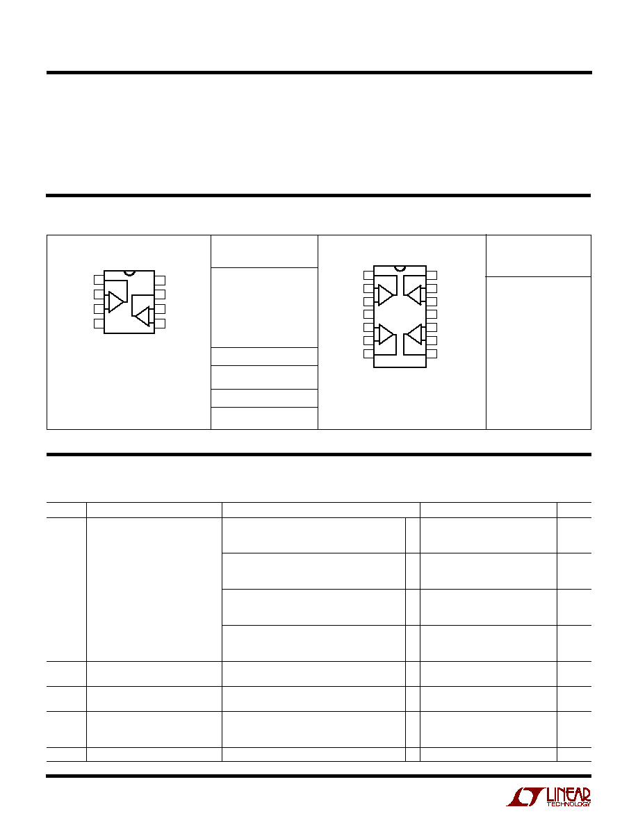
PACKAGE/ORDER I
N
FOR
M
ATIO
N
W
U
U
ORDER PART
NUMBER
Consult factory for Military grade parts.
LT1491CN
LT1491CS
LT1491IN
LT1491IS
TOP VIEW
S PACKAGE
14-LEAD PLASTIC SO
N PACKAGE
14-LEAD PDIP
1
2
3
4
5
6
7
14
13
12
11
10
9
8
A
B
C
OUT A
≠IN A
+IN A
V
+
+IN B
≠IN B
OUT B
OUT D
≠IN D
+IN D
V
≠
+IN C
≠ IN C
OUT C
D
T
JMAX
= 150
∞
C,
JA
= 110
∞
C/ W (N)
T
JMAX
= 150
∞
C,
JA
= 150
∞
C/ W (S)
T
JMAX
= 150
∞
C,
JA
= 250
∞
C/ W (MS8)
T
JMAX
= 150
∞
C,
JA
= 130
∞
C/ W (N8)
T
JMAX
= 150
∞
C,
JA
= 190
∞
C/ W (S8)
1
2
3
4
8
7
6
5
TOP VIEW
MS8 PACKAGE
8-LEAD MSOP
N8 PACKAGE
8-LEAD PDIP
S8 PACKAGE
8-LEAD PLASTIC SO
V
+
OUT B
≠IN B
+IN B
A
B
OUT A
≠IN A
+IN A
V
≠
S8 PART MARKING
MS8 PART MARKING
ORDER PART
NUMBER
LTBB
1490 1490I
LT1490CMS8
LT1490CN8
LT1490CS8
LT1490IN8
LT1490IS8
ABSOLUTE AXI U RATI GS
W
W
W
U
(Note 1)
SYMBOL
PARAMETER
CONDITIONS
MIN
TYP
MAX
UNITS
V
OS
Input Offset Voltage
LT1490 N Package
220
800
µ
V
0
∞
C
T
A
70
∞
C
q
1000
µ
V
≠ 40
∞
C
T
A
85
∞
C
q
1100
µ
V
LT1490 S Package
220
950
µ
V
0
∞
C
T
A
70
∞
C
q
1200
µ
V
≠ 40
∞
C
T
A
85
∞
C
q
1300
µ
V
LT1491 N Package
300
1100
µ
V
0
∞
C
T
A
70
∞
C
q
1350
µ
V
≠ 40
∞
C
T
A
85
∞
C
q
1450
µ
V
LT1490CMS8 Package, LT1491 S Package
350
1450
µ
V
0
∞
C
T
A
70
∞
C
q
1650
µ
V
≠ 40
∞
C
T
A
85
∞
C
q
1750
µ
V
V
OS
TC
Input Offset Voltage Drift
0
∞
C
T
A
70
∞
C (Note 7)
q
2
4
µ
V/
∞
C
≠40
∞
C
T
A
85
∞
C (Note 7)
q
2
4
µ
V/
∞
C
I
OS
Input Offset Current
q
0.2
0.8
nA
V
CM
= 44V (Note 4)
q
0.8
µ
A
I
B
Input Bias Current
q
4
8
nA
V
CM
= 44V (Note 4)
q
4
10
µ
A
V
S
= 0V
0.1
nA
Input Noise Voltage
0.1Hz to 10Hz
1
µ
V
P-P
ELECTRICAL CHARACTERISTICS
The
q
denotes specifications which apply over the full operating temperature
range, otherwise specifications are at T
A
= 25
∞
C. V
S
= 3V, 0V; V
S
= 5V, 0V; V
CM
= V
OUT
= half supply, unless otherwise noted. (Note 3)
(For new designs, use the LT1490A or LT1491A)
3
LT1490/LT1491
SYMBOL
PARAMETER
CONDITIONS
MIN
TYP
MAX
UNITS
e
n
Input Noise Voltage Density
f = 1kHz
50
nV/
Hz
i
n
Input Noise Current Density
f = 1kHz
0.03
pA/
Hz
R
IN
Input Resistance
Differential
6
17
M
Common Mode, V
CM
= 0V to 44V
4
11
M
C
IN
Input Capacitance
4.6
pF
Input Voltage Range
q
0
44
V
CMRR
Common Mode Rejection Ratio
V
CM
= 0V to V
CC
≠ 1V
q
84
98
dB
(Note 4)
V
CM
= 0V to 44V
q
80
98
dB
A
VOL
Large-Signal Voltage Gain
V
S
= 3V, V
O
= 500mV to 2.5V, R
L
= 10k
200
1500
V/mV
0
∞
C
T
A
70
∞
C
q
133
V/mV
≠ 40
∞
C
T
A
85
∞
C
q
100
V/mV
V
S
= 5V, V
O
= 500mV to 4.5V, R
L
= 10k
400
1500
V/mV
0
∞
C
T
A
70
∞
C
q
250
V/mV
≠ 40
∞
C
T
A
85
∞
C
q
200
V/mV
V
OL
Output Voltage Swing Low
V
S
= 3V, No Load
q
22
50
mV
V
S
= 3V, I
SINK
= 5mA
q
250
450
mV
V
S
= 5V, No Load
q
22
50
mV
V
S
= 5V, I
SINK
= 5mA
q
250
500
mV
V
S
= 5V, I
SINK
= 10mA
330
500
mV
V
OH
Output Voltage Swing High
V
S
= 3V, No Load
q
2.95
2.978
V
V
S
= 3V, I
SOURCE
= 5mA
q
2.55
2.6
V
V
S
= 5V, No Load
q
4.95
4.978
V
V
S
= 5V, I
SOURCE
= 10mA
q
4.30
4.6
V
I
SC
Short-Circuit Current (Note 2)
V
S
= 3V, Short to GND
10
15
mA
V
S
= 3V, Short to V
CC
10
30
mA
V
S
= 5V, Short to GND
15
25
mA
V
S
= 5V, Short to V
CC
15
30
mA
PSRR
Power Supply Rejection Ratio
V
S
= 2.5V to 12.5V, V
CM
= V
O
= 1V
q
84
98
dB
Minimum Operating Supply Voltage
q
2
2.5
V
Reverse Supply Voltage
I
S
= ≠ 100
µ
A per Amplifier
q
18
27
V
I
S
Supply Current per Amplifier
40
50
µ
A
(Note 5)
q
55
µ
A
GBW
Gain Bandwidth Product
f = 1kHz
110
180
kHz
(Note 4)
0
∞
C
T
A
70
∞
C
q
100
kHz
≠ 40
∞
C
T
A
85
∞
C
q
90
kHz
SR
Slew Rate
A
V
= ≠ 1, R
L
=
0.035
0.06
V/
µ
s
(Note 6)
0
∞
C
T
A
70
∞
C
q
0.031
V/
µ
s
≠ 40
∞
C
T
A
85
∞
C
q
0.030
V/
µ
s
ELECTRICAL CHARACTERISTICS
The
q
denotes specifications which apply over the full operating temperature
range, otherwise specifications are at T
A
= 25
∞
C. V
S
= 3V, 0V; V
S
= 5V, 0V; V
CM
= V
OUT
= half supply, unless otherwise noted. (Note 3)

4
LT1490/LT1491
SYMBOL
PARAMETER
CONDITIONS
MIN
TYP
MAX
UNITS
V
OS
Input Offset Voltage
LT1490 N, S Package
250
1200
µ
V
0
∞
C
T
A
70
∞
C
q
1400
µ
V
≠ 40
∞
C
T
A
85
∞
C
q
1500
µ
V
LT1491 N Package
350
1250
µ
V
0
∞
C
T
A
70
∞
C
q
1500
µ
V
≠ 40
∞
C
T
A
85
∞
C
q
1600
µ
V
LT1490CMS8 Package, LT1491 S Package
400
1600
µ
V
0
∞
C
T
A
70
∞
C
q
1850
µ
V
≠ 40
∞
C
T
A
85
∞
C
q
1950
µ
V
V
OS
TC
Input Offset Voltage Drift
0
∞
C
T
A
70
∞
C (Note 7)
q
3
6
µ
V/
∞
C
≠ 40
∞
C
T
A
85
∞
C (Note 7)
q
3
6
µ
V/
∞
C
I
OS
Input Offset Current
q
0.2
0.8
nA
I
B
Input Bias Current
q
4
8
nA
Input Noise Voltage
0.1Hz to 10Hz
1
µ
V
P-P
e
n
Input Noise Voltage Density
f = 1kHz
50
nV/
Hz
i
n
Input Noise Current Density
f = 1kHz
0.03
pA/
Hz
R
IN
Input Resistance
Differential
6
17
M
Common Mode, V
CM
= ≠ 15V to 14V
15000
M
C
IN
Input Capacitance
4.6
pF
Input Voltage Range
q
≠ 15
29
V
CMRR
Common Mode Rejection Ratio
V
CM
= ≠ 15V to 29V
q
80
98
dB
A
VOL
Large-Signal Voltage Gain
V
O
=
±
14V, R
L
= 10k
100
250
V/mV
0
∞
C
T
A
70
∞
C
q
75
V/mV
≠ 40
∞
C
T
A
85
∞
C
q
50
V/mV
V
O
Output Voltage Swing
No Load
q
±
14.9
±
14.978
V
I
OUT
=
±
5mA
q
±
14.5
±
14.750
V
I
OUT
=
±
10mA
±
14.5
±
14.670
V
I
SC
Short-Circuit Current (Note 2)
Short to GND
±
20
±
25
mA
0
∞
C
T
A
70
∞
C
q
±
15
mA
≠ 40
∞
C
T
A
85
∞
C
q
±
10
mA
PSRR
Power Supply Rejection Ratio
V
S
=
±
1.25V to
±
22V
q
88
98
dB
I
S
Supply Current per Amplifier
50
70
µ
A
q
85
µ
A
GBW
Gain Bandwidth Product
f = 1kHz
125
200
kHz
0
∞
C
T
A
70
∞
C
q
110
kHz
≠ 40
∞
C
T
A
85
∞
C
q
100
kHz
SR
Slew Rate
A
V
= ≠ 1, R
L
=
,
V
O
=
±
10V,
0.0375
0.07
V/
µ
s
Measure at V
O
=
±
5V
0
∞
C
T
A
70
∞
C
q
0.0330
V/
µ
s
≠ 40
∞
C
T
A
85
∞
C
q
0.0300
V/
µ
s
Note 1: Absolute Maximum Ratings are those values beyond which the
life of the device may be impaired.
Note 2: A heat sink may be required to keep the junction temperature
below absolute maximum. This depends on the power supply voltage
and how many amplifiers are shorted.
Note 3: The LT1490C/LT1491C are guaranteed to meet specified
performance from 0
∞
C to 70
∞
C. The LT1490C/LT1491C are designed,
characterized and expected to meet specified performance from ≠ 40
∞
C
to 85
∞
C but are not tested or QA sampled at these temperatures.
The LT1490I/LT1491I are guaranteed to meet specified performance from
≠ 40
∞
C to 85
∞
C.
Note 4: V
S
= 5V limits are guaranteed by correlation to V
S
= 3V and
V
S
=
±
15V tests.
Note 5: V
S
= 3V limits are guaranteed by correlation to V
S
= 5V and
V
S
=
±
15V tests.
Note 6: Guaranteed by correlation to slew rate at V
S
=
±
15V and GBW
at V
S
= 3V and V
S
=
±
15V tests.
Note 7: This parameter is not 100% tested.
ELECTRICAL CHARACTERISTICS
The
q
denotes specifications which apply over the full operating temperature
range, otherwise specifications are at T
A
= 25
∞
C. V
S
=
±
15V, V
CM
= 0V, V
OUT
= 0V, unless otherwise noted. (Note 3)

5
LT1490/LT1491
TOTAL SUPPLY VOLTAGE (V)
0
0
SUPPLY CURRENT PER AMPLIFIER (
µ
A)
10
30
40
50
70
10
20
25
45
1490/91 G01
20
80
60
5
15
30
35
40
T
A
= 125
∞
C
T
A
= 25
∞
C
T
A
= ≠55
∞
C
Supply Current vs Supply Voltage
COMMON MODE VOLTAGE (V)
4.0
INPUT BIAS CURRENT (nA)
2000
6000
5.6
1490/91 G03
30
10
4000
20
0
≠10
4.4
4.8
5.2
44
T
A
=
125
∞
C
T
A
=
≠55
∞
C
T
A
=
25
∞
C
V
S
= 5V, 0V
TOTAL SUPPLY VOLTAGE (V)
0
CHANGE IN INPUT OFFSET VOLTAGE (
µ
V)
200
400
4
1490/91 G02
0
≠200
100
300
≠100
≠300
≠ 400
1
2
3
5
T
A
=
25
∞
C
T
A
=
125
∞
C
T
A
=
≠55
∞
C
Minimum Supply Voltage
Input Bias Current
vs Common Mode Voltage
Output Saturation Voltage
vs Input Overdrive
SOURCING LOAD CURRENT (mA)
0.001
0.01
0.1
1
10
0.01
OUTPUT SATURATION VOLTAGE (V)
0.1
1
1490/90 G04
V
S
=
±
2.5V
V
OD
= 30mV
T
A
= ≠ 55
∞
C
T
A
= 125
∞
C
T
A
= 25
∞
C
Output Saturation Voltage
vs Load Current (Output High)
Output Saturation Voltage
vs Load Current (Output Low)
SINKING LOAD CURRENT (mA)
0.001
0.01
0.1
1
10
0.01
OUTPUT SATURATION VOLTAGE (V)
0.1
1
1490/90 G05
V
S
=
±
2.5V
V
OD
= 30mV
T
A
= ≠ 55
∞
C
T
A
= 125
∞
C
T
A
= 25
∞
C
INPUT OVERDRIVE (mV)
0
OUTPUT SATURATION VOLTAGE (mV)
60
80
100
80
1490/91 G06
40
20
50
70
90
30
10
0
20
40
60
10
90
30
50
70
100
V
S
=
±
2.5V
NO LOAD
OUTPUT HIGH
OUTPUT LOW
0.1Hz to 10Hz Noise Voltage
FREQUENCY (Hz)
1
40
INPUT NOISE VOLTAGE DENSITY (nV/
Hz)
50
60
70
10
100
1k
1490/91 G08
30
80
FREQUENCY (Hz)
1
INPUT NOISE CURRENT DENSITY (pA/
Hz)
10
100
1k
1490/91 G09
0.20
0.25
0.30
0.35
0.15
0.10
0.05
0
TIME (SEC)
NOISE VOLTAGE (400nV/DIV)
2
4
6
8
1490 G07
10
1
0
3
5
7
9
V
S
=
±
2.5V
Noise Voltage Density
vs Frequency
Input Noise Current vs Frequency
TYPICAL PERFOR A CE CHARACTERISTICS
U
W

6
LT1490/LT1491
FREQUENCY (kHz)
1
10
GAIN (dB)
PHASE SHIFT (DEG)
20
30
40
50
10
100
1000
1490/91 G10
0
≠10
≠20
≠30
60
70
≠20
0
20
40
60
≠ 40
≠ 60
≠ 80
≠100
80
100
V
S
=
±
2.5V
PHASE
GAIN
Gain and Phase Shift
vs Frequency
Slew Rate vs Temperature
Gain Bandwidth Product
vs Temperature
Gain Bandwidth Product and
Phase Margin vs Supply Voltage
PSRR vs Frequency
Gain Bandwidth Product and
Phase Margin vs Load Resistance
CMRR vs Frequency
Channel Separation vs Frequency
Output Impedance vs Frequency
TEMPERATURE (
∞
C)
≠50
SLEW RATE (V/
µ
s)
0
50
75
1490/91 G12
0.04
0.06
0.10
0.12
0.08
≠25
25
100
125
RISING, V
S
=
±
15V
RISING, V
S
=
±
1.5V
FALLING, V
S
=
±
1.5V
FALLING, V
S
=
±
15V
TOTAL SUPPLY VOLTAGE (V)
0
150
GAIN BANDWIDTH PRODUCT (kHz)
PHASE MARGIN (DEG)
160
180
190
200
250
220
10
20
25
45
1490/91 G13
170
230
240
210
10
30
60
20
50
40
5
15
30
35
40
R
L
= 10k
f = 1kHz
PHASE MARGIN
GAIN BANDWIDTH
FREQUENCY (kHz)
1
COMMON MODE REJECTION RATIO (dB)
10
120
100
80
60
40
20
100
1490 G14
V
S
=
±
15V
V
S
=
±
1.5V
FREQUENCY (kHz)
1
≠20
POWER SUPPLY REJECTION RATIO (dB)
0
20
40
60
10
100
1490/91 G15
≠10
10
30
50
70
80
V
S
=
±
2.5V
POSITIVE SUPPLY
NEGATIVE SUPPLY
LOAD RESISTANCE (k
)
1
50
GAIN BANDWIDTH PRODUCT (kHz)
PHASE MARGIN (DEG)
100
150
200
250
350
10
100
1490/91 G16
300
20
30
40
50
60
80
70
V
S
=
±
2.5V
A
V
= ≠1
R
F
= R
G
= 100k
f = 1kHz
PHASE MARGIN
GAIN BANDWIDTH
FREQUENCY (kHz)
0.1
90
CHANNEL SEPARATION (dB)
100
110
120
130
1
10
100
1490/91 G17
80
70
50
40
60
V
S
=
±
15V
FREQUENCY (kHz)
0.1
OUTPUT IMPEDANCE (
)
100
1k
10k
1
10
100
1490/91 G18
10
1
0.1
V
S
=
±
2.5V
A
V
= 100
A
V
= 10
A
V
= 1
TEMPERATURE (
∞
C)
≠50
GAIN BANDWIDTH PRODUCT (kHz) 120
140
160
260
200
0
50
75
1490/91 G11
100
220
240
180
≠25
25
100
125
V
S
=
±
15V
V
S
=
±
3V
f = 1kHz
TYPICAL PERFOR A CE CHARACTERISTICS
U
W

7
LT1490/LT1491
Open-Loop Gain
Large-Signal Response
Small-Signal Response
OUTPUT VOLTAGE (5V/DIV)
≠10V
0V
10V
1490/91 G25
CHANGE IN INPUT OFFSET VOLTAGE
(100
µ
V/DIV)
V
S
=
±
15V
1490/91 G26
1490/91 G27
R
L
= 2k
R
L
= 50k
Undistorted Output Swing
vs Frequency
Settling Time to 0.1%
vs Output Step
Capacitive Load Handling,
Overshoot vs Capacitive Load
Total Harmonic Distortion + Noise
vs Frequency
Total Harmonic Distortion + Noise
vs Load Resistance
FREQUENCY (kHz)
0.1
20
OUTPUT SWING (V
P-P
)
25
30
35
1
10
100
1490/91 G19
15
10
5
0
DISTORTION
1%
V
S
=
±
15V
V
S
=
±
2.5V
SETTLING TIME (
µ
s)
0
≠10
OUTPUT STEP (V)
≠8
≠ 4
≠2
0
10
4
40
80
100
1490/91 F20
≠ 6
6
8
2
20
60
120 140
160
V
S
=
±
15V
A
V
= ≠1
A
V
= ≠1
A
V
= 1
A
V
= 1
FREQUENCY (kHz)
0.01
THD + NOISE (%)
0.1
1
10
0.01
1
10
1490/91 G22
0.001
0.1
V
S
= 3V, 0V
V
OUT
= 2V
P-P
V
CM
= 1.2V
R
L
= 50k
A
V
= ≠1
A
V
= 1
LOAD RESISTANCE TO GROUND (k
)
0.01
THD + NOISE (%)
0.1
1
10
0.1
10
100
1490/91 G23
0.001
1
V
S
= 3V TOTAL
A
V
= 1
V
IN
= 2V
P-P
AT 1kHz
V
S
=
±
1.5V
V
IN
=
±
1V
V
S
= 3V, 0V
V
IN
= 0.5V TO 2.5V
V
S
= 3V, 0V
V
IN
= 0.2V TO 2.2V
OUTPUT VOLTAGE (V
P-P
)
0.01
THD + NOISE (%)
1
10
0
2
3
1490/91 G24
0.001
1
0.1
R
L
= 10k
V
CM
= HALF SUPPLY
f = 1kHz
A
V
= 1
V
S
= 3V, 0V
A
V
= ≠1
V
S
= 3V, 0V
A
V
= ≠1
V
S
=
±
1.5V
A
V
= 1
V
S
=
±
1.5V
Total Harmonic Distortion + Noise
vs Output Voltage
R
L
= 10k
V
S
=
±
15V
A
V
= ≠1
V
S
=
±
15V
A
V
= 1
CAPACITIVE LOAD (pF)
20
OVERSHOOT (%)
40
60
50
80
100
10
30
70
90
10
100
1000
10000
1490/91 G21
0
V
S
= 5V, 0V
I
SOURCE
= 170
µ
A
A
V
= 1
A
V
= 2
A
V
= 5
A
V
= 10
TYPICAL PERFOR A CE CHARACTERISTICS
U
W

8
LT1490/LT1491
Supply Voltage
The positive supply pin of the LT1490/LT1491 should be
bypassed with a small capacitor (about 0.01
µ
F) within an
inch of the pin. When driving heavy loads an additional
4.7
µ
F electrolytic capacitor should be used. When using
split supplies, the same is true for the negative supply pin.
The LT1490/LT1491 are protected against reverse battery
voltages up to 18V. In the event a reverse battery condition
occurs, the supply current is less than 1nA.
The LT1490/LT1491 can be shut down by removing V
+
. In
this condition the input bias current is less than 0.1nA,
even if the inputs are 44V above the negative supply.
When operating the LT1490/LT1491 on total supplies of
30V or more, the supply must not be brought up faster
than 1
µ
s. This is especially true if low ESR bypass capaci-
tors are used. A series RLC circuit is formed from the
supply lead inductance and the bypass capacitor. 5
of
resistance in the supply or the bypass capacitor will
dampen the tuned circuit enough to limit the rise time.
Inputs
The LT1490/LT1491 have two input stages, NPN and PNP
(see the Simplified Schematic), resulting in three distinct
operating regions as shown in the Input Bias Current vs
Common Mode typical performance curve.
For input voltages about 0.8V or more below V
+
, the PNP
input stage is active and the input bias current is typically
≠ 4nA. When the input voltage is about 0.5V or less from
V
+
, the NPN input stage is operating and the input bias
current is typically 18nA. Increases in temperature will
cause the voltage at which operation switches from the
PNP stage to the NPN stage to move towards V
+
. The input
offset voltage of the NPN stage is untrimmed and is
typically 600
µ
V.
A Schottky diode in the collector of each NPN transistor of
the NPN input stage allows the LT1490/LT1491 to operate
with either or both of its inputs above V
+
. At about 0.3V
above V
+
the NPN input transistor is fully saturated and the
input bias current is typically 4
µ
A at room temperature.
The input offset voltage is typically 700
µ
V when operating
above V
+
. The LT1490/LT1491 will operate with its inputs
44V above V
≠
regardless of V
+
.
The inputs are protected against excursions as much as
22V below V
≠
by an internal 1k resistor in series with each
input and a diode from the input to the negative supply.
There is no output phase reversal for inputs up to 22V
below V
≠
. There are no clamping diodes between the
inputs and the maximum differential input voltage is 44V.
Output
The output voltage swing of the LT1490/LT1491 is af-
fected by input overdrive as shown in the typical perfor-
mance curves. When monitoring voltages within 100mV
of either rail, gain should be taken to keep the output from
clipping.
The output of the LT1490/LT1491 can be pulled up to 18V
beyond V
+
with less than 1nA of leakage current, provided
that V
+
is less than 0.5V.
The normally reverse-biased substrate diode from the
output to V
≠
will cause unlimited currents to flow when the
output is forced below V
≠
. If the current is transient and
limited to 100mA, no damage will occur.
The LT1490/LT1491 is internally compensated to drive at
least 200pF of capacitance under any output loading
conditions. A 0.22
µ
F capacitor in series with a 150
resistor between the output and ground will compensate
these amplifiers for larger capacitive loads, up to 10,000pF,
at all output currents.
Distortion
There are two main contributors of distortion in op amps:
output crossover distortion as the output transitions from
sourcing to sinking current and distortion caused by
nonlinear common mode rejection. Of course, if the op
amp is operating inverting there is no common mode
induced distortion. When the LT1490 switches between
input stages there is significant nonlinearity in the CMRR.
Lower load resistance increases the output crossover
distortion, but has no effect on the input stage transition
distortion. For lowest distortion the LT1490/LT1491 should
be operated single supply, with the output always sourc-
ing current and with the input voltage swing between
ground and (V
+
≠ 0.8V). See the Typical Performance
Characteristics curves.
APPLICATIO S I FOR ATIO
W
U
U
U

9
LT1490/LT1491
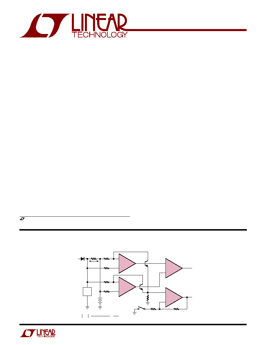
Gain
The open-loop gain is almost independent of load when
the output is sourcing current. This optimizes perfor-
mance in single supply applications where the load is
returned to ground. The typical performance photo of
Open-Loop Gain for various loads shows the details.
≠
+
V
OUT
1490/91 TA02
100k
100k
C
0.1
µ
F
V
OUT
= 5V
P-P
WITH 5V SUPPLY
I
S
= 200
µ
A
59k
1/2 LT1490
5V
R
50k
f = 1
2RC
AT V
S
= 5V, R = 50k, C = 1nF
OUTPUT IS 5kHz SLEW LIMITED TRIANGLE WAVE
≠
+
V
IN
1490/91 TA04
0.22
µ
F
C
L
10,000pF
150
1/2 LT1490
Square Wave Oscillator
Optional Output Compensation for
Capacitive Loads Greater Than 200pF
Q10
D5
Q9
Q1
Q7
R2
1k
R3
1k
R4
40k
Q8
Q5
≠ IN
+IN
Q11
Q12
D4
ONE AMPLIFIER
D2
Q2
D1
Q6
Q13
Q14
R1
30k
R5
40k
Q4
2
µ
A
+
Q15
Q19
D3
Q3
Q16
Q18
Q22
V
+
Q17
Q20
Q21
OUT
V
≠
1490/91 SS
APPLICATIO S I FOR ATIO
W
U
U
U
TYPICAL APPLICATIO S
U
SI PLIFIED SCHE ATIC
W
W

10
LT1490/LT1491
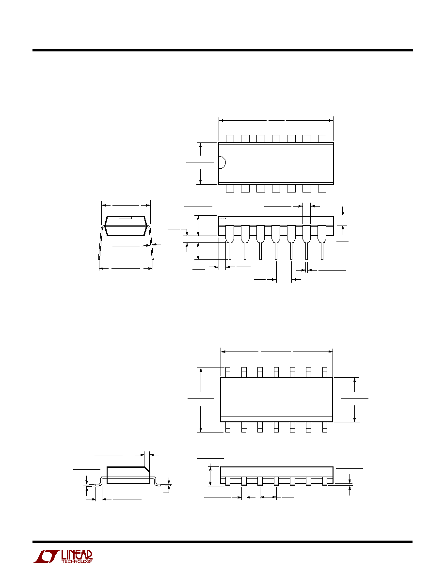
Dimensions in inches (millimeters) unless otherwise noted.
MS Package
8-Lead Plastic MSOP
(LTC DWG # 05-08-1660)
S8 Package
8-Lead Plastic Small Outline (Narrow 0.150)
(LTC DWG # 05-08-1610)
N8 Package
8-Lead PDIP (Narrow 0.300)
(LTC DWG # 05-08-1510)
MSOP (MS8) 1098
* DIMENSION DOES NOT INCLUDE MOLD FLASH, PROTRUSIONS OR GATE BURRS. MOLD FLASH,
PROTRUSIONS OR GATE BURRS SHALL NOT EXCEED 0.006" (0.152mm) PER SIDE
** DIMENSION DOES NOT INCLUDE INTERLEAD FLASH OR PROTRUSIONS.
INTERLEAD FLASH OR PROTRUSIONS SHALL NOT EXCEED 0.006" (0.152mm) PER SIDE
0.021
±
0.006
(0.53
±
0.015)
0
∞
≠ 6
∞
TYP
SEATING
PLANE
0.007
(0.18)
0.040
±
0.006
(1.02
±
0.15)
0.012
(0.30)
REF
0.006
±
0.004
(0.15
±
0.102)
0.034
±
0.004
(0.86
±
0.102)
0.0256
(0.65)
BSC
1
2
3
4
0.193
±
0.006
(4.90
±
0.15)
8
7 6
5
0.118
±
0.004*
(3.00
±
0.102)
0.118
±
0.004**
(3.00
±
0.102)
N8 1098
0.009 ≠ 0.015
(0.229 ≠ 0.381)
0.300 ≠ 0.325
(7.620 ≠ 8.255)
0.325
+0.035
≠0.015
+0.889
≠0.381
8.255
(
)
0.100
(2.54)
BSC
0.065
(1.651)
TYP
0.045 ≠ 0.065
(1.143 ≠ 1.651)
0.130
±
0.005
(3.302
±
0.127)
0.020
(0.508)
MIN
0.018
±
0.003
(0.457
±
0.076)
0.125
(3.175)
MIN
1
2
3
4
8
7
6
5
0.255
±
0.015*
(6.477
±
0.381)
0.400*
(10.160)
MAX
*THESE DIMENSIONS DO NOT INCLUDE MOLD FLASH OR PROTRUSIONS.
MOLD FLASH OR PROTRUSIONS SHALL NOT EXCEED 0.010 INCH (0.254mm)
0.016 ≠ 0.050
(0.406 ≠ 1.270)
0.010 ≠ 0.020
(0.254 ≠ 0.508)
◊
45
∞
0
∞
≠ 8
∞
TYP
0.008 ≠ 0.010
(0.203 ≠ 0.254)
SO8 1298
0.053 ≠ 0.069
(1.346 ≠ 1.752)
0.014 ≠ 0.019
(0.355 ≠ 0.483)
TYP
0.004 ≠ 0.010
(0.101 ≠ 0.254)
0.050
(1.270)
BSC
1
2
3
4
0.150 ≠ 0.157**
(3.810 ≠ 3.988)
8
7
6
5
0.189 ≠ 0.197*
(4.801 ≠ 5.004)
0.228 ≠ 0.244
(5.791 ≠ 6.197)
DIMENSION DOES NOT INCLUDE MOLD FLASH. MOLD FLASH
SHALL NOT EXCEED 0.006" (0.152mm) PER SIDE
DIMENSION DOES NOT INCLUDE INTERLEAD FLASH. INTERLEAD
FLASH SHALL NOT EXCEED 0.010" (0.254mm) PER SIDE
*
**
U
PACKAGE DESCRIPTIO
11
LT1490/LT1491
Dimensions in inches (millimeters) unless otherwise noted.
N Package
14-Lead PDIP (Narrow 0.300)
(LTC DWG # 05-08-1510)
S Package
14-Lead Plastic Small Outline (Narrow 0.150)
(LTC DWG # 05-08-1610)
Information furnished by Linear Technology Corporation is believed to be accurate and reliable.
However, no responsibility is assumed for its use. Linear Technology Corporation makes no represen-
tation that the interconnection of its circuits as described herein will not infringe on existing patent rights.
N14 1098
0.020
(0.508)
MIN
0.125
(3.175)
MIN
0.130
±
0.005
(3.302
±
0.127)
0.045 ≠ 0.065
(1.143 ≠ 1.651)
0.065
(1.651)
TYP
0.018
±
0.003
(0.457
±
0.076)
0.100
(2.54)
BSC
0.005
(0.125)
MIN
0.255
±
0.015*
(6.477
±
0.381)
0.770*
(19.558)
MAX
3
1
2
4
5
6
7
8
9
10
11
12
13
14
0.009 ≠ 0.015
(0.229 ≠ 0.381)
0.300 ≠ 0.325
(7.620 ≠ 8.255)
0.325
+0.035
≠0.015
+0.889
≠0.381
8.255
(
)
*THESE DIMENSIONS DO NOT INCLUDE MOLD FLASH OR PROTRUSIONS.
MOLD FLASH OR PROTRUSIONS SHALL NOT EXCEED 0.010 INCH (0.254mm)
1
2
3
4
0.150 ≠ 0.157**
(3.810 ≠ 3.988)
14
13
0.337 ≠ 0.344*
(8.560 ≠ 8.738)
0.228 ≠ 0.244
(5.791 ≠ 6.197)
12
11
10
9
5
6
7
8
0.016 ≠ 0.050
(0.406 ≠ 1.270)
0.010 ≠ 0.020
(0.254 ≠ 0.508)
◊
45
∞
0
∞
≠ 8
∞
TYP
0.008 ≠ 0.010
(0.203 ≠ 0.254)
S14 1298
0.053 ≠ 0.069
(1.346 ≠ 1.752)
0.014 ≠ 0.019
(0.355 ≠ 0.483)
TYP
0.004 ≠ 0.010
(0.101 ≠ 0.254)
0.050
(1.270)
BSC
DIMENSION DOES NOT INCLUDE MOLD FLASH. MOLD FLASH
SHALL NOT EXCEED 0.006" (0.152mm) PER SIDE
DIMENSION DOES NOT INCLUDE INTERLEAD FLASH. INTERLEAD
FLASH SHALL NOT EXCEED 0.010" (0.254mm) PER SIDE
*
**
U
PACKAGE DESCRIPTIO
12
LT1490/LT1491
14901fb LT/LCG 0600 2K REV B ∑ PRINTED IN USA
©
LINEAR TECHNOLOGY CORPORATION 1996
PART NUMBER
DESCRIPTION
COMMENTS
LT1078/LT1079
Dual/Quad 55
µ
A Max, Single Supply, Precision Op Amps
Input/Output Common Mode Includes Ground, 70
µ
V V
OS(MAX)
and 2.5
µ
V/
∞
C Drift (Max), 200kHz GBW, 0.07V/
µ
s Slew Rate
LTC1152
Rail-to-Rail Input, Rail-to-Rail Output, Zero-Drift Amplifier
High DC Accuracy, 10
µ
V V
OS(MAX)
, 100nV/
∞
C, 1MHz GBW,
1V/
µ
s Slew Rate, Supply Current 2.2mA (Max), Single Supply,
Can Be Configured for C-Load
TM
Operation
LT1178/LT1179
Dual/Quad 17
µ
A Max, Single Supply, Precison Op Amps
Input/Output Common Mode Includes Ground, 70
µ
V V
OS(MAX)
and 4
µ
V/
∞
C Drift (Max), 85kHz GBW, 0.04V/
µ
s Slew Rate
LT1366/LT1367
Dual/Quad Precision, Rail-to-Rail Input and Output Op Amps
475
µ
V V
OS(MAX)
, 500V/mV A
VOL(MIN)
, 400kHz GBW
LT1490A/LT1491A
Dual/Quad Micropower Rail-to-Rail Precision Op Amps
500
µ
V V
OS(MAX)
, Improved Version of the LT1490/LT1491
C-Load is a trademark of Linear Technology Corporation.
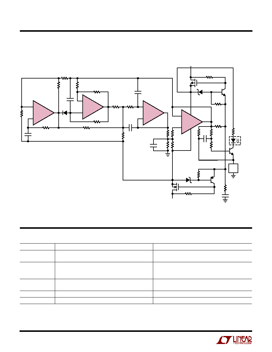
Ring-Tone Generator
RELATED PARTS
≠
+
≠
+
≠
+
≠
+
1490/1491 TA03
R6
10k
R2
47k
R7
16k
R8
620k
R4
1.6M
R1
33k
R3
10k
R5
100k
R10
620k
C4
0.068
µ
F
9
10
6
7
8
1
5
C3
0.047
µ
F
C5
0.01
µ
F
R13
130k
R12
10k
R15
47k
R14
10k
R24
420
C7
47
µ
F
LOAD
UP TO
TEN
PHONES
R23
4.7k
R26
2k
Q5
2N3904
Q4
2N3906
Q2
IRF9620
≠180V
POWER AMPLIFIER
SMOOTHING FILTER
20Hz OSCILLATOR
CADENCE OSCILLATOR
*LED OF OPTO1 ILLUMINATES WHEN THE PHONE IS OFF THE HOOK
SEE DESIGN NOTE DN134 FOR AN EXPLANATION OF THE CIRCUIT
R18
100
R17
620
R16
100k
Z1
15V
100k
R25
4.7k
C6
0.033
µ
F
R21
150
R19
620
Z2
15V
R9
300k
R11
10k
D1
1N4148
C2
0.47
µ
F
C1
1
µ
F
2
3
1/4 LT1491
1/4 LT1491
12
4
11
13
Q1
IRF628
Q3
2N3904
60V
14
1/4 LT1491
1/4 LT1491
OPTO1*
R20
100k
Linear Technology Corporation
1630 McCarthy Blvd., Milpitas, CA 95035-7417
q
(408) 432-1900
FAX: (408) 434-0507
q
TELEX: 499-3977
q
www.linear-tech.com
TYPICAL APPLICATIO
U