
1
LT1500/LT1501
Adaptive-Frequency
Current Mode Switching Regulators
FEATURES
DESCRIPTIO
N
U
The LT
Æ
1500 is an adaptive-frequency current mode step-
up switching regulator with an internal power switch that
is rated up to 700mA. In contrast to pulse skipping
switching regulators, the LT1500 uses a current mode
topology that provides lower noise operation and im-
proved efficiency. Only at very light loads is Burst Mode
TM
activated to give high efficiency and micropower opera-
tion. High switching frequency (up to 500kHz) allows very
small inductors to be used, along with ceramic capacitors
if desired.
The LT1500 operates with input voltages from 1.8V to 15V
and has only 200
µ
A operating current dropping to 8
µ
A in
shutdown. A low-battery comparator is included which
stays alive in shutdown. A second output feedback pin
with negative polarity allows negative output voltages to
be regulated when the switcher is connected up as a Cuk
or a flyback converter.
Two package types are available. The LT1500 comes in a
14-pin SO package, with two options available for fixed
output (3.3V or 5V) or adjustable operation. A reduced
feature part, the LT1501, comes in the smaller 8-pin SO
package with internal frequency compensation. It is also
available in adjustable and fixed output voltage versions.
s
Low Noise Adaptive-Frequency Current Mode
Operation Avoids Low Frequency Noise at
Most Load Currents
s
Can Be Externally Synchronized (LT1500)
s
Micropower Quiescent Current: 200
µ
A
s
Shutdown Current: 8
µ
A Typ
s
Internal Loop Compensation
s
Low-Battery Comparator Active in Shutdown
s
Minimum Input Voltage: 1.8V Typ
s
Additional Negative Voltage Feedback Pin (LT1500)
s
Up to 500kHz Switching Frequency
s
Uses Low Profile, Low Cost Surface Mount Inductors
, LTC and LT are registered trademarks of Linear Technology Corporation.
Burst Mode is a trademark of Linear Technology Corporation.
s
Portable Instrumentation
s
Battery Operated Systems
s
PDA's
s
Standby Power
APPLICATIO
N
S
U
TYPICAL APPLICATIO
N
U
2-Cell to 5V Converter
SHDN
V
IN
LBO
LBI
SW
I
SENSE
GND
OUT
LT1501-5
+
1nF
301k
1%
301k
1%
LOW-BATTERY FLAG
(USE EXTERNAL PULL-UP)
33
µ
F*
6V
+
220
µ
F**
10V
TANT
2 EACH
NiCd OR
ALKALINE
CELLS
22
µ
H
5V, 200mA
LT1500/01 ∑ TA01
AVX, TPSC107M006R0150
AVX, TPSD107M010 R0100
SUMIDA CD73-220, CD54-220
OR CD43-220. SELECT ACCORDING
TO MAXIMUM LOAD CURRENT
*
**
D1
MBR0520L
2
LT1500/LT1501
ABSOLUTE
M
AXI
M
U
M
RATINGS
W
W
W
U
Supply Voltage ........................................................ 20V
Switch Voltage (SW)................................................ 30V
Shutdown Voltage (SHDN) ...................................... 20V
I
SENSE
Voltage .......................................................... 20V
FB Voltage ................................................................. 5V
LBI Voltage ................................................................ 5V
LBO Voltage ............................................................. 15V
Operating Ambient Temperature Range
Commercial ............................................. 0
∞
C to 70
∞
C
Industrial ............................................ ≠ 40
∞
C to 85
∞
C
Operating Junction Temperature Range
Commercial ........................................... 0
∞
C to 100
∞
C
Industrial .......................................... ≠ 40
∞
C to 100
∞
C
Storage Temperature Range ................. ≠ 65
∞
C to 150
∞
C
Lead Temperature (Soldering, 10 sec).................. 300
∞
C
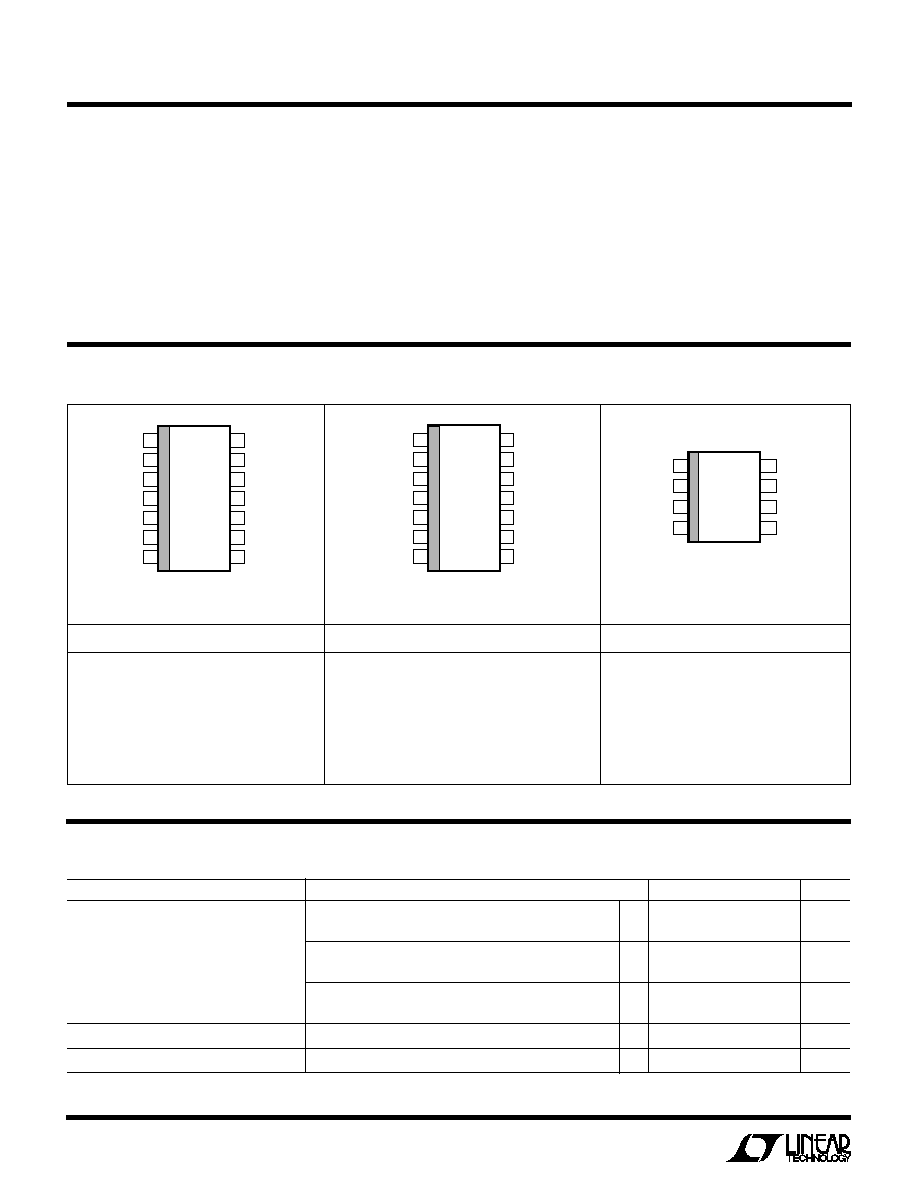
PACKAGE/ORDER I
N
FOR
M
ATIO
N
W
U
U
T
JMAX
= 100
∞
C,
JA
= 100
∞
C/ W
ORDER PART NUMBER
ORDER PART NUMBER
ORDER PART NUMBER
LT1500CS-3/5
LT1500IS-3/5
Consult factory for Military grade parts.
ELECTRICAL CHARACTERISTICS
T
J
= 25
∞
C, V
IN
= 2.3V unless otherwise noted.
PARAMETER
CONDITIONS
MIN
TYP
MAX
UNITS
Feedback/Output Pin Reference Voltage
LT1500/LT1501, T
J
= 25
∞
C
1.240
1.265
1.290
V
All Conditions (Note 6)
q
1.235
1.295
V
LT1500-3/5, Select Pin Open
3.230
3.300
3.370
V
All Conditions (Note 6)
q
3.200
3.400
V
LT1500-3/5, Select Pin Grounded
4.900
5.000
5.100
V
All Conditions (Note 6)
q
4.85
5.15
V
Reference Voltage Line Regulation
V
IN
= 2.3V to 15V
q
0.02
0.06
%/V
Feedback Pin Bias Current
q
30
100
nA
T
JMAX
= 100
∞
C,
JA
= 100
∞
C/ W
LT1500CS
LT1500IS
T
JMAX
= 100
∞
C,
JA
= 120
∞
C/ W
1
2
3
4
8
7
6
5
TOP VIEW
FB/OUT
LBI
LBO
SW
SHDN
V
IN
I
SENSE
GND
S8 PACKAGE
8-LEAD PLASTIC SO
LT1501CS8
LT1501CS8-3.3
LT1501CS8-5
LT1501IS8
LT1501IS8-3.3
LT1501IS8-5
TOP VIEW
S PACKAGE
14-LEAD PLASTIC SO
1
2
3
4
5
6
7
14
13
12
11
10
9
8
SHDN
V
C
V
IN
I
SENSE
NC
GND
PGND
FB
NFB
SS
LBI
LBO
SYNC
SW
TOP VIEW
S PACKAGE
14-LEAD PLASTIC SO
1
2
3
4
5
6
7
14
13
12
11
10
9
8
SHDN
V
C
V
IN
I
SENSE
NC
GND
PGND
V
OUT
(3.3V/5V)
SELECT
SS
LBI
LBO
SYNC
SW

3
LT1500/LT1501
ELECTRICAL CHARACTERISTICS
T
J
= 25
∞
C, V
IN
= 2.3V unless otherwise noted.
PARAMETER
CONDITIONS
MIN
TYP
MAX
UNITS
Internal Divider Current
LT1500-3.3/LT1501-3.3
q
22
30
µ
A
LT1500-5/LT1501-5
q
33
45
µ
A
Operating Quiescent Current
V
IN
5V, V
SHDN
= 2.3V (Note 1)
q
200
280
µ
A
V
IN
= 15V
q
320
µ
A
Supply Current in Shutdown
V
SHDN
0.2V, Fixed Voltages (Note 7)
T
J
0
∞
C
q
8
15
µ
A
T
J
< 0
∞
C
20
µ
A
Shutdown Pin Threshold
q
0.4
1.1
V
Shutdown Pin Input Current
V
SHDN
= 2.3V
q
3
10
µ
A
Input Start-Up Voltage
V
SHDN
= V
IN
T
J
0
∞
C
q
2.0
2.1
V
T
J
< 0
∞
C
2.2
V
Undervoltage Lockout
Light Load
1.8
V
Full Load
2.0
2.1
V
Power Switch
Switch On Resistance
I
SW
= 0.7A (Note 2)
q
0.50
0.72
Peak Switch Current (Note 3)
q
0.7
0.85
1.3
A
Switch Breakdown Voltage
I
SW
= 100
µ
A
q
30
45
V
Switch Leakage Current
V
SW
= 5V
q
0.2
5
µ
A
V
SW
= 20V
q
0.3
10
µ
A
Switch Turn-On Delay (Note 5)
800
ns
Switch Turn-Off Delay (Note 5)
400
ns
Current Sense Resistor
q
0.28
0.42
Low-Battery Comparator
Low-Battery Threshold
Falling Edge
q
1.20
1.24
1.28
V
Threshold Hysteresis
20
mV
LBI Input Bias Current
q
20
50
nA
LBO Output Low State
V
LBI
= 1.2V, I
SINK
= 100
µ
A
q
0.1
0.25
V
I
SINK
= 2mA
q
0.3
0.5
V
LBO Leakage Current
V
LBI
= 1.3V, V
LBO
15V
q
2
µ
A
LT1500 Functions
SYNC Pin Bias Current
V
SYNC
= 3.3V
q
15
35
µ
A
SYNC Pin Threshold
q
0.4
1.3
V
Error Amplifier Transconductance
600
µ
mho
V
C
Pin Source Current
20
µ
A
V
C
Pin High Clamp Voltage
1.20
1.26
1.32
V
NFB Reference Voltage
FB Pin Open
q
1.230
1.265
1.300
V
NFB Pin Bias Current
q
12
20
µ
A
NFB to FB Transconductance
Note 4
10,000
µ
mho
Soft Start Bias Current
Current Flows Out of Pin
q
2
4
7
µ
A
4
LT1500/LT1501
ELECTRICAL CHARACTERISTICS
The
q
denotes specifications which apply over the full operating
temperature range.
Note 1: Feedback pin or output is held sightly above the regulated value to
force the V
C
node low and switching to stop.
Note 2: See Typical Performance Characteristics for graph of Guaranteed
Switch Voltage vs Saturation Voltage.
Note 3: Peak switch current is the guaranteed minimum value of switch
current available in normal operation. Highest calculated switch current at
full load should not exceed the minimum value shown.
Note 4: Loading on FB pin will affect NFB reference voltage.
V
NFB
= I
FB
/gm.
Do not exceed 10
µ
A loading on FB when NFB is being used.
Note 5: This is the delay between sense pin current reaching its upper or
lower threshold and switch transition. Switch delay times cause peak-to-
peak inductor current to increase and therefore switching frequency to be
low. This effect will be significant for frequencies above 100kHz. See
Application Information and Typical Performance Characteristics.
Note 6: Reference voltage under all conditions includes V
IN
= 2.1V to 15V,
all loads and full temperature range.
Note 7: As with all boost regulators the output voltage of the LT1500
cannot fall to less than input voltage because of the path through the catch
diode. This means that the output voltage divider on adjustable parts will
still be generating feedback voltage at the FB pin (fixed voltage parts have
an internal switch to disconnect the divider in shutdown). If the voltage on
FB is greater than 0.6V in shutdown, the internal error amplifier will draw
current that adds to shutdown current. See graph of Shutdown Current vs
FB voltage in Typical Performance Characteristics.
TYPICAL PERFOR
M
A
N
CE CHARACTERISTICS
U
W
Switching Frequency
(3.3V Output)
LOAD CURRENT (mA)
0
50
100
10
FREQUENCY (kHz)
100
1000
150
200
250
300
LTC1500/01 ∑ TPC20
10
µ
H
20
µ
H
50
µ
H
100
µ
H
BURST REGION
VIN = 2.3V
Switching Frequency (5V Output)
LOAD CURRENT (mA)
0
50
100
10
FREQUENCY (kHz)
100
1000
150
200
250
300
LTC1500/01 ∑ TPC21
10
µ
H
20
µ
H
50
µ
H
100
µ
H
BURST REGION
VIN = 3V
Switching Frequency (12V Output)
LOAD CURRENT (mA)
0
25
50
75
FREQUENCY (kHz)
1000
100
10
100 125 150 175
200
LTC1500/01 ∑ TPC22
10
µ
H
50
µ
H
20
µ
H
100
µ
H
BURST REGION
VIN = 5V
Efficiency (3.3V Output)
LOAD CURRENT (mA)
1
EFFICIENCY (%)
100
90
80
70
60
50
40
30
10
100
1000
LTC1500/01 ∑ TPC17
T
J
= 25
∞
C
V
IN
= 2.3V
LOW LOSS INDUCTOR
L = 100
µ
H
L = 10
µ
H
L = 33
µ
H
Efficiency (5V Output)
LOAD CURRENT (mA)
1
EFFICIENCY (%)
100
90
80
70
60
50
40
30
10
100
1000
LTC1500/01 ∑ TPC18
V
IN
= 3V
LOW LOSS INDUCTOR
L = 100
µ
H
L = 10
µ
H
L = 33
µ
H
Efficiency (12V Output)
LOAD CURRENT (mA)
1
EFFICIENCY (%)
100
90
80
70
60
50
40
30
10
100
1000
LTC1500/01 ∑ TPC19
V
IN
= 5V
LOW LOSS INDUCTOR
L = 100
µ
H
L = 10
µ
H
L = 33
µ
H
5
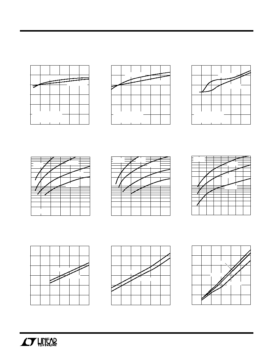
LT1500/LT1501
TYPICAL PERFOR
M
A
N
CE CHARACTERISTICS
U
W
Efficiency (3.3V Output)
I
LOAD
= 100mA
I
LOAD
= 10mA
INPUT VOLTAGE (V)
1.75
EFFICIENCY (%)
100
90
80
70
60
50
40
2.00
2.25
2.50
2.75
LT1500/01 ∑ TPC11
3.00
3.25
T
J
= 25
∞
C
L = 33
µ
H
LOW LOSS INDUCTOR
Efficiency (5V Output)
I
LOAD
= 100mA
I
LOAD
= 10mA
INPUT VOLTAGE (V)
2.0
EFFICIENCY (%)
100
90
80
70
60
50
40
2.5
3.0
3.5
4.0
LT1500/01 ∑ TPC12
4.5
5.0
T
J
= 25
∞
C
L = 33
µ
H
LOW LOSS INDUCTOR
Efficiency (12V Output)
I
LOAD
= 50mA
I
LOAD
= 10mA
INPUT VOLTAGE (V)
0
EFFICIENCY (%)
100
90
80
70
60
50
40
2
4
6
8
LT1500/01 ∑ TPC13
10
12
T
J
= 25
∞
C
L = 33
µ
H
LOW LOSS INDUCTOR
Inductor Copper Loss (5V Output)
Inductor Copper Loss
(3.3V Output)
LOAD CURRENT (mA)
0
50
100
0.1
EFFICIENCY LOSS (%)
1
10
150
200
250
300
LT1500/01 ∑ TPC14
R = 1
R = 0.5
R = 0.2
R = 0.1
V
IN
= 2.3V
LOAD CURRENT (mA)
0
50
100
0.1
EFFICIENCY LOSS (%)
1
10
150
200
250
300
LT1500/01 ∑ TPC15
R = 0.5
R = 0.2
R = 1
V
IN
= 3V
R = 0.1
Inductor Copper Loss
(12V Output)
LOAD CURRENT (mA)
0
25
50
75
EFFICIENCY LOSS (%)
10
1
0.1
100 125 150 175
200
LTC1500/01 ∑ TPC16
R = 0.2
R = 0.5
R = 1
V
IN
= 5V
Maximum Load Current
(3.3V Output)
INPUT VOLTAGE (V)
1.50
OUTPUT CURRENT (mA)
600
500
400
300
200
100
0
1.75
2.00
2.25
2.50
LT1500/01 ∑ TPC08
2.75
3.00
L
33
µ
H
L = 10
µ
H
Maximum Load Current
(5V Output)
INPUT VOLTAGE (V)
2.0
OUTPUT CURRENT (mA)
600
500
400
300
200
100
0
2.5
3.0
3.5
4.0
LT1500/01 ∑ TPC09
4.5
5.0
L
33
µ
H
L = 10
µ
H
Maximum Load Current
(12V Output)
L = 100
µ
H
INPUT VOLTAGE (V)
0
OUTPUT CURRENT (mA)
600
500
400
300
200
100
0
2
4
6
8
LT1500/01 ∑ TPC10
10
12
L = 33
µ
H
L = 10
µ
H