Äîêóìåíòàöèÿ è îïèñàíèÿ www.docs.chipfind.ru
1
LT1505
TYPICAL APPLICATIO
N
U
DESCRIPTIO
U
FEATURES
APPLICATIO S
U
Constant-Current/Voltage
High Efficiency Battery Charger
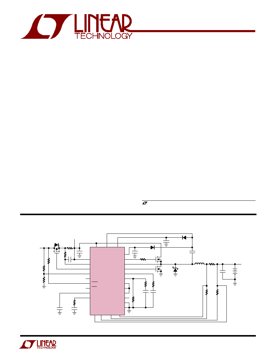
Figure 1. Low Dropout 4A Lithium-Ion Battery Charger
s
Simple Charging of Li-Ion, NiMH and NiCd Batteries
s
Very High Efficiency: Up to 97%
s
Precision 0.5% Charging Voltage Accuracy
s
Preset Battery Voltages: 12.3V, 12.6V,
16.4V and 16.8V
s
5% Charging Current Accuracy
s
Charging Current Programmed by Resistor or DAC
s
0.5V Dropout Voltage, Duty Cycle > 99.5%
s
AC Adapter Current Limit* Maximizes Charging Rate
s
Flag Indicates Li-Ion Charge Completion
s
Auto Shutdown with Adapter Removal
s
Only 10
µ
A Battery Drain When Idle
s
Synchronizable Up to 280kHz
The LT
®
1505 PWM battery charger controller fast charges
multiple battery chemistries including lithium-ion (Li-Ion),
nickel-metal-hydride (NiMH) and nickel-cadmium (NiCd)
using constant-current or constant-voltage control. Maxi-
mum current can be easily programmed by resistors or a
DAC. The constant-voltage output can be selected for 3 or 4
series Li-Ion cells with 0.5% accuracy.
A third control loop limits the current drawn from the AC
adapter during charging*. This allows simultaneous opera-
tion of the equipment and fast battery charging without over-
loading the AC adapter.
The LT1505 can charge batteries ranging from 2.5V to 20V
with dropout voltage as low as 0.5V. Synchronous
N-channel FETs switching at 200kHz give high efficiency
and allow small inductor size. A diode is not required in
series with the battery because the charger automatically
enters a 10
µ
A sleep mode when the wall adapter is un-
plugged. A logic output indicates Li-Ion full charge when
current drops to 20% of the programmed value.
The LT1505 is available in a 28-pin SSOP package.
s
Notebook Computers
s
Portable Instruments
s
Chargers for Li-Ion, NiMH, NiCd and Lead Acid
Rechargeable Batteries
, LTC and LT are registered trademarks of Linear Technology Corporation.
5
C
PROG
1
µ
F
300
C7
0.68
µ
F
C6
0.1
µ
F
C3
2.2
µ
F
C
OUT
22
µ
F
25V
×
2
C2
0.68
µ
F
V
BAT
12.6V
BATTERY
NOTE: DBODY IS THE BODY DIODE OF M3
C
IN
: SANYO OS-CON
L1: SUMIDA CDRH127-150
(CAN BE FROM 10
µ
H TO 30
µ
H)
M1
Si4412
M2
Si4412
D4
MBRS140
D2
MMSD4148T1
D3
MMSD4148T1
R7
500
100k
R5
4k
R1
1k
R6
4k
*BODY DIODE
POLARITY MUST
BE AS SHOWN
R
S4
0.025
M3
Si4435
DBODY*
TO
SYSTEM POWER
V
IN
(FROM
ADAPTER)
R
S1
0.025
L1
15
µ
H
1505 F01
R
PROG
4.93k
1%
0.33
µ
F
R
X4
3k
R
S2
200
1%
R
S3
200
1%
C
IN
47
µ
F
35V
C1
1
µ
F
C4
0.1
µ
F
BAT2 BAT
SENSE
LT1505
V
CC
BOOST
BOOSTC
SPIN
PGND
AGND
4.1V
4.2V
V
FB
3 CELL
PROG
V
C
BGATE
COMP1
CAP
FLAG
SHDN
SYNC
UV
INFET
SW
TGATE
GBIAS
CLP
CLN
*US Patent No. 5,723,970
2
LT1505
V
CC
, CLP, CLN, INFET, UV, 3CELL, FLAG ................ 27V
SW Voltage with Respect to GND ........................... 2V
BOOST, BOOSTC Voltage with Respect to V
CC
....... 10V
GBIAS ..................................................................... 10V
SYNC, BAT2, BAT, SENSE, SPIN ............................ 20V
V
C
, PROG, V
FB
, 4.1V, 4.2V ........................................ 7V
CAP, SHDN ..........................................................
±
3mA
ABSOLUTE
M
AXI
M
U
M
RATINGS
W
W
W
U
(Note 1)
TGATE, BGATE Current Continuous ....................... 0.2A
TGATE, BGATE Output Energy (per cycle) ............... 2
µ
J
Maximum Operating V
CC
......................................... 24V
Operating Ambient Temperature Range ....... 0
°
C to 70
°
C
Operating Junction Temperature Range .... 0
°
C to 125
°
C
Storage Temperature Range ................. 65
°
C to 150
°
C
Lead Temperature (Soldering, 10 sec).................. 300
°
C
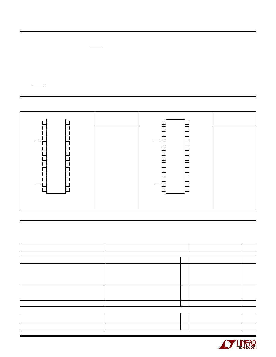
ORDER PART
NUMBER
LT1505CG
LT1505CG-1
ORDER PART
NUMBER
T
JMAX
= 125
°
C,
JA
= 100
°
C/ W
Consult factory for Industrial and Military grade parts.
1
2
3
4
5
6
7
8
9
10
11
12
13
14
TOP VIEW
G PACKAGE
28-LEAD PLASTIC SSOP
28
27
26
25
24
23
22
21
20
19
18
17
16
15
BOOST
TGATE
SW
SYNC
SHDN
AGND
UV
INFET
CLP
CLN
COMP1
CAP
FLAG
4.1V
PGND
BGATE
GBIAS
BOOSTC
V
CC
BAT
SPIN
SENSE
BAT2
PROG
V
C
V
FB
3CELL
4.2V
T
JMAX
= 125
°
C,
JA
= 100
°
C/ W
1
2
3
4
5
6
7
8
9
10
11
12
13
14
TOP VIEW
G PACKAGE
28-LEAD PLASTIC SSOP
28
27
26
25
24
23
22
21
20
19
18
17
16
15
BOOST
TGATE
SW
SYNC
SHDN
AGND
UV
INFET
NC
NC
GND
CAP
FLAG
4.1V
PGND
BGATE
GBIAS
BOOSTC
V
CC
BAT
SPIN
SENSE
BAT2
PROG
V
C
V
FB
3CELL
4.2V
NOTE: LT1505CG-1 DOES NOT
HAVE INPUT CURRENT
LIMITING FUNCTION.
ELECTRICAL CHARACTERISTICS
PACKAGE/ORDER I
N
FOR
M
ATIO
N
W
U
U
The
q
denotes specifications which apply over the full operating
temperature range, otherwise specifications are at T
A
= 25
°
C. V
CC
= 18V, V
BAT
= 12.6V, V
CLN
= V
CC
(LT1505), no load on any
outputs unless otherwise noted.
PARAMETER
CONDITIONS
MIN
TYP
MAX
UNITS
Overall
Supply Current
V
CC
24V
q
12
15
mA
Sense Amplifier CA1 Gain and Input Offset Voltage
11V
V
CC
24V , 0V
V
BAT
20V
(With R
S2
= 200
, R
S3
= 200
)
R
PROG
= 4.93k
95
100
105
mV
(Measured across R
S1
, Figure 1) (Note 2)
R
PROG
= 4.93k
q
92
108
mV
R
PROG
= 49.3k
7
10
13
mV
BOOST Pin Current
V
BOOST
= V
SW
+ 8V, 0V
V
SW
20V
TGATE High
2
3
mA
TGATE Low
2
3
mA
BOOSTC Pin Current
V
BOOSTC
= V
CC
+ 8V
1
mA
Reference
Reference Voltage (Note 3)
R
PROG
= 4.93k, Measured at V
FB
with V
A
2.453
2.465
2.477
V
Supplying I
PROG
and Switching Off
Reference Voltage Tolerance
11V
V
CC
24V
q
2.441
2.489
V
3
LT1505
PARAMETER
CONDITIONS
MIN
TYP
MAX
UNITS
Preset Battery Voltage (12.3V, 16.4V, 12.6V, 16.8V)
All Preset Battery Voltages
Measured at BAT2 Pin
0.5
%
Preset Battery Voltage Tolerance
(V
BAT
+ 0.3V)
V
CC
24V
q
1
1
%
BAT2 Pin Input Current
V
BAT2
= V
PRESET
1V
q
6
µ
A
Voltage Setting Resistors Tolerance (R4, R5, R6, R7)
40
40
%
Shutdown
Undervoltage Lockout (TGATE and BGATE "Off")
Measured at UV Pin
q
6.3
6.7
7.15
V
Threshold (Note 9)
UV Pin Input Current
0V
V
UV
8V
q
1
5
µ
A
Reverse Current from Battery in Micropower
V
BAT
20V, V
UV
0.4V,
10
30
µ
A
Shutdown (Note 10)
V
CC
= V
SW
= Battery Voltage
Shutdown Threshold at SHDN Pin When V
CC
q
1
2
V
is Connected
SHDN Pin Current
0V
V
SHDN
3V
8
µ
A
Supply Current in Shutdown
V
CC
24V
15
20
mA
(V
SHDN
is Low, V
CC
is Connected)
Minimum I
PROG
for Switching "On"
1
4
22
µ
A
Minimum I
PROG
for Switching "Off" at V
PROG
1V
q
1
2.4
mA
Current Sense Amplifier CA1 Inputs (SENSE, BAT)
Input Bias Current (SENSE, BAT)
V
SHDN
= High
q
50
120
µ
A
V
SHDN
= Low (Shutdown)
10
µ
A
Input Common Mode Low
q
0.25
V
Input Common Mode High
q
V
CC
0.3
V
SPIN Input Current
V
SHDN
= High, V
SPIN
2V (Note 8)
q
2
mA
V
SHDN
= Low (Shutdown)
10
µ
A
Oscillator
Switching Frequency (f
NOM
)
180
200
220
kHz
Switching Frequency Tolerance
q
170
200
230
kHz
SYNC Pin Input Current
V
SYNC
= 0V
0.5
mA
V
SYNC
= 2V
30
µ
A
Synchronization Pulse Threshold on SYNC Pin
0.9
1.2
2.0
V
Synchronization Frequency
q
240
280
kHz
Maximum Duty Cycle
V
BOOST
Threshold to Turn TGATE Off
Measured at (V
BOOST
V
SW
)
(Comparator A2) (Note 4)
Low to High
q
6.8
7.1
7.3
V
Hysteresis
0.25
V
Maximum Duty Cycle of Natural Frequency 200kHz
q
85
90
%
(Note 5)
Current Amplifier CA2
Transconductance
V
C
= 1V, I
VC
=
±
1
µ
A
150
200
300
µ
mho
Maximum V
C
for Switch Off
q
0.6
V
I
VC
Current (Out of Pin)
V
C
0.6V
q
50
µ
A
V
C
< 0.45V
q
3
mA
V
C
at Shutdown
V
SHDN
= Low (Shutdown)
q
0.35
V
ELECTRICAL CHARACTERISTICS
The
q
denotes specifications which apply over the full operating
temperature range, otherwise specifications are at T
A
= 25
°
C. V
CC
= 18V, V
BAT
= 12.6V, V
CLN
= V
CC
(LT1505), no load on any
outputs unless otherwise noted.
4
LT1505
Note 6: See "Lithium-Ion Charging Completion" in the Applications
Information Section.
Note 7: Tested with Test Circuit 3.
Note 8: I
SPIN
keeps switching on to keep V
BAT
regulated when battery is
not present to avoid high surge current from C
OUT
when battery is
inserted.
Note 9: Above undervoltage threshold switching is enabled.
Note 10: Do not connect V
CC
directly to V
IN
(see Figure 1). This connection
will cause the internal diode between V
BAT
and V
CC
to be forward-biased
and may cause high current to flow from V
IN
. When the adapter is
removed, V
CC
will be held up by the body diode of M1.
Note 1: Absolute Maximum Ratings are those values beyond which the life
of a device may be impaired.
Note 2: Tested with Test Circuit 1.
Note 3: Tested with Test Circuit 2.
Note 4: When V
CC
and battery voltage differential is low, high duty factor
is required. The LT1505 achieves a duty factor greater than 99% by
skipping cycles. Only when V
BOOST
drops below the comparator A2
threshold will TGATE be turned off. See Applications Information.
Note 5: When the system starts, C2 (boost cap) has to be charged up to
drive TGATE and to start the system. The LT1505 will keep TGATE off and
turn BGATE on for 0.2
µ
s at 200kHz to charge up C2. Comparator A2
senses V
BOOST
and switches to the normal PWM mode when V
BOOST
is
above the threshold.
ELECTRICAL CHARACTERISTICS
The
q
denotes specifications which apply over the full operating
temperature range, otherwise specifications are at T
A
= 25
°
C. V
CC
= 18V, V
BAT
= 12.6V, V
CLN
= V
CC
(LT1505), no load on any
outputs unless otherwise noted.
PARAMETER
CONDITIONS
MIN
TYP
MAX
UNITS
Voltage Amplifier VA
Transconductance (Note 3)
Output Current from 50
µ
A to 500
µ
A
0.21
0.6
1.0
mho
Output Source Current
V
FB
= V
PROG
= V
REF
+ 10mV
1.1
mA
V
FB
Input Bias Current
At 0.5mA VA Output Current, T
A
= 25
°
C
±
3
±
10
nA
At 0.5mA VA Output Current, T
A
= 70
°
C
10
25
nA
(3 CELL, 4.1V, 4.2V Are Not Connected, V
BAT2
= 0V)
Current Limit Amplifier CL1
Turn-On Threshold
0.5mA Output Current
87
92
97
mV
Transconductance
Output Current from 50
µ
A to 500
µ
A
0.5
1
3
mho
CLP Input Current
0.5mA Output Current
1
3
µ
A
CLN Input Current
0.5mA Output Current
0.8
2
mA
Input P-Channel FET Driver (INFET)
INFET "On" Clamping Voltage (V
CC
V
INFET
)
V
CC
11V
q
6.5
7.8
9
V
INFET "On" Driver Current
V
INFET
= V
CC
6V
q
8
20
mA
INFET "Off" Clamping Voltage (V
CC
V
INFET
)
V
CC
Not Connected, I
INFET
< 2
µ
A
1.4
V
INFET "Off" Drive Current
V
CC
Not Connected, (V
CC
V
INFET
)
2V
2.5
mA
Charging Completion Flag (Comparator E6)
Charging Completion Threshold (Note 6)
Measured at V
RS1
, V
CAP
= 2V (Note 7)
14
20
28
mV
Threshold On CAP Pin
Low to High Threshold
q
3.3
4.2
V
High to Low Threshold
q
0.6
V
V
CAP
at Shutdown
V
SHDN
= Low (Shutdown)
q
0.13
0.3
V
FLAG (Open Collector) Output Low
V
CAP
= 4V, I
FLAG
< 1mA
q
0.3
V
FLAG Pin Leakage Current
V
CAP
= 0.6V
q
3
µ
A
Gate Drivers (TGATE, BGATE)
V
GBIAS
11V < V
CC
< 24V, I
GBIAS
15mA
q
8.4
8.9
9.3
V
V
SHDN
= Low (Shutdown)
q
1
3
V
V
TGATE
High (V
TGATE
V
SW
)
I
TGATE
20mA, V
BOOST
= V
GBIAS
0.5V
q
5.6
6.6
V
V
BGATE
High
I
BGATE
20mA
q
6.2
7.2
V
V
TGATE
Low (V
TGATE
V
SW
)
I
TGATE
50mA
q
0.8
V
V
BGATE
Low
I
BGATE
50mA
q
0.8
V
Peak Gate Drive Current
10nF Load
1
A
Gate Drive Rise and Fall Time
1nF Load
25
ns
V
TGATE
, V
BGATE
at Shutdown
V
SHDN
= Low (Shutdown)
q
1
V
I
TGATE
= I
BGATE
= 10
µ
A
5
LT1505
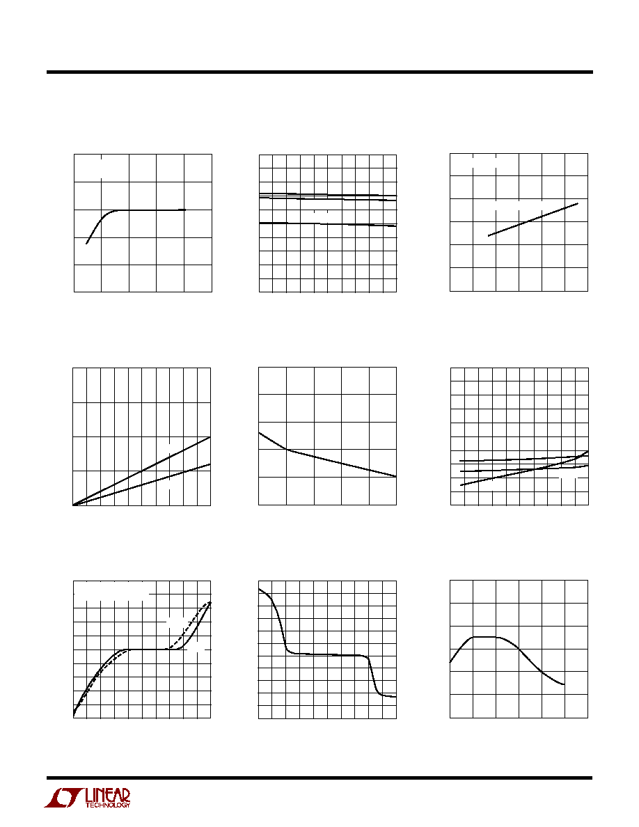
TYPICAL PERFOR
M
A
N
CE CHARACTERISTICS
U
W
I
BAT
(A)
0
EFFICIENCY (%)
105
100
95
90
85
80
4
1505 G01
1
2
3
5
V
IN
= 19V
V
BAT
= 12.6V
Efficiency of Figure 1 Circuit
I
VA
(mA)
0
V
FB
(mV)
4
3
2
1
0
0.8
1505 G04
0.2
0.1
0.3
0.5
0.7
0.9
0.4
0.6
1.0
125
°
C
25
°
C
V
CC
(V)
15
14
13
12
11
10
I
CC
(mA)
1505 G06
10
13
16
19
22
25
0
°
C
25
°
C
125
°
C
I
GBIAS
(mA)
9.2
9.1
9.0
8.9
8.8
8.7
8.6
8.5
8.4
8.3
8.1
V
GBIAS
(V)
1505 G02
0
2 4 6 8 10 12 14 16 18 20
0
°
C
25
°
C
125
°
C
V
GBIAS
vs I
GBIAS
V
FB
vs I
VA
(Voltage Amplifier)
TEMPERATURE (
°
C)
0
25
50
75
100
THRESHOLD (mV)
125
1505 G05
98
96
94
92
90
88
Current Limit Amplifier
CL1 Threshold
I
CC
vs V
CC
JUNCTION TEMPERATURE (
°
C)
0
REFERENCE VOLTAGE (V)
2.470
2.468
2.466
2.464
2.462
2.460
2.458
25
50
75
100
1505 G09
125
150
Reference Voltage vs Temperature
V
PROG
(V)
0
1
2
3
5
4
I
PROG
(mA)
6
0
6
1505 G07
125
°
C
CURRENT FEEDBACK
AMPLIFIER OPEN LOOP
25
°
C
PROG Pin Characteristics
V
C
(V)
1.2
1.0
0.8
0.6
0.4
0.2
0
0.2
0.4
0.6
0.8
1.0
I
VC
(mA)
1505 G08
0
0.4 0.6
0.2
0.8 1.0 1.2 1.4 1.6 1.8 2.0
V
C
Pin Characteristics
V
REF
Line Regulation
V
CC
(V)
0
V
REF
(V)
0.003
0.002
0.001
0
0.001
0.002
0.003
5
10
15
20
1505 G03
25
30
ALL TEMPERATURES
0
°
C
T
J
125
°
C