 | –≠–ª–µ–∫—Ç—Ä–æ–Ω–Ω—ã–π –∫–æ–º–ø–æ–Ω–µ–Ω—Ç: LT1510C | –°–∫–∞—á–∞—Ç—å:  PDF PDF  ZIP ZIP |
1
LT1510/LT1510-5
Constant-Voltage/
Constant-Current Battery Charger
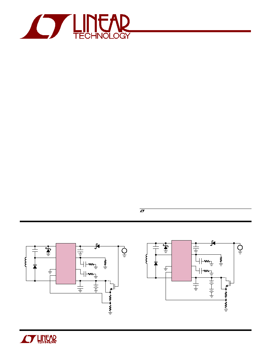
Figure 2. Charging Lithium Batteries (Efficiency at 1.3A > 87%)
* NiCd and NiMH batteries require charge termination circuitry (not shown in Figure 1).
TYPICAL APPLICATIO
N
S
U
, LTC and LT are registered trademarks of Linear Technology Corporation.
plest, most efficient solution to fast-charge modern re-
chargeable batteries including lithium-ion (Li-Ion), nickel-
metal-hydride (NiMH)* and nickel-cadmium (NiCd)* that
require constant-current and/or constant-voltage charg-
ing. The internal switch is capable of delivering 1.5A DC
current (2A peak current). The 0.1
onboard current
sense resistor makes the charging current programming
very simple. One resistor (or a programming current from
a DAC) is required to set the full charging current (1.5A) to
within 5% accuracy. The LT1510 with 0.5% reference
voltage accuracy meets the critical constant-voltage charg-
ing requirement for lithium cells.
The LT1510 can charge batteries ranging from 2V to 20V.
Ground sensing of current is not required and the battery's
negative terminal can be tied directly to ground. A saturat-
ing switch running at 200kHz (500kHz for LT1510-5) gives
high charging efficiency and small inductor size. A block-
ing diode is not required between the chip and the battery
because the chip goes into sleep mode and drains only 3
µ
A
when the wall adaptor is unplugged. Soft start and shutdown
features are also provided. The LT1510 is available in a 16-pin
fused lead power SO package with a thermal resistance of
50
∞
C/W, an 8-pin SO and a 16-pin PDIP.
FEATURES
s
Charges NiCd, NiMH and Lithium-Ion Batteries ≠≠
Only One
1
/
10
W Resistor Is Needed to Program
Charging Current
s
High Efficiency Current Mode PWM with 1.5A
Internal Switch and Sense Resistor
s
3% Typical Charging Current Accuracy
s
Precision 0.5% Voltage Reference for Voltage
Mode Charging or Overvoltage Protection
s
Current Sensing Can Be at Either Terminal of
the Battery
s
Low Reverse Battery Drain Current: 3
µ
A
s
Charging Current Soft Start
s
Shutdown Control
s
500kHz Version Uses Small Inductor
With switching frequency as high as 500kHz, The LT
Æ
1510
current mode PWM battery charger is the smallest, sim-
APPLICATIO
N
S
U
DESCRIPTIO
N
U
s
Chargers for NiCd, NiMH and Lithium Batteries
s
Step-Down Switching Regulator with Precision
Adjustable Current Limit
Figure 1. 500kHz Smallest Li-Ion Cell Phone Charger (0.8A)
SW
BOOST
GND
SENSE
V
CC
PROG
V
C
BAT
6.19k
8.2V TO 20V
+
R3
70.6k
0.25%
R4
100k
0.25%
Q3
2N7002
NOTE: COMPLETE LITHIUM-ION CHARGER, NO TERMINATION REQUIRED
TOKIN OR MARCON CERAMIC SURFACE MOUNT
COILTRONICS TP3-100, 10
µ
H, 2.2mm HEIGHT (0.8A CHARGING CURRENT)
COILTRONICS TP1 SERIES, 10
µ
H, 1.8mm HEIGHT (<0.5A CHARGING CURRENT)
PANASONIC EEFCD1B220
OPTIONAL, SEE APPLICATIONS INFORMATION
1510 F01
C1
0.22
µ
F
C
IN
*
10
µ
F
L1**
10
µ
H
LT1510-5
D1
MBRM120T3
D3
MBRM120T3
D2
MMBD914L
OVP
+
C
OUT***
22
µ
F
4.2V
+
+
≠
0.1
µ
F
1k
1
µ
F
300
*
**
***
SW
BOOST
GND
SENSE
V
CC
PROG
V
C
BAT
3.83k
11V TO 28V
+
+
R3
240k
0.25%
R4
100k
0.25%
Q3
VN2222
NOTE: COMPLETE LITHIUM-ION CHARGER, NO TERMINATION REQUIRED
* TOKIN OR MARCON CERAMIC SURFACE MOUNT
** COILTRONICS CTX33-2
OPTIONAL, SEE APPLICATIONS INFORMATION
1510 F02
C1
0.22
µ
F
C
IN
*
10
µ
F
L1**
33
µ
H
LT1510
D1
1N5819
D3
1N5819
D2
1N914
OVP
+
C
OUT
22
µ
F
TANT
4.2V
4.2V
+
+
≠
0.1
µ
F
1k
1
µ
F
300
2
LT1510/LT1510-5
Supply Voltage (V
MAX
) ............................................ 30V
Switch Voltage with Respect to GND ...................... ≠ 3V
Boost Pin Voltage with Respect to V
CC
................... 30V
Boost Pin Voltage with Respect to GND ................. ≠ 5V
V
C
, PROG, OVP Pin Voltage ...................................... 8V
I
BAT
(Average) ........................................................ 1.5A
Switch Current (Peak)............................................... 2A
Storage Temperature Range ................. ≠ 65
∞
C to 150
∞
C
ABSOLUTE
M
AXI
M
U
M
RATINGS
W
W
W
U
Operating Ambient Temperature Range
Commercial ............................................. 0
∞
C to 70
∞
C
Extended Commercial (Note 7) ........... ≠ 40
∞
C to 85
∞
C
Industrial (Note 8) .............................. ≠ 40
∞
C to 85
∞
C
Operating Junction Temperature Range
LT1510C (Note 7) ............................. ≠ 40
∞
C to 125
∞
C
LT1510I ............................................ ≠ 40
∞
C to 125
∞
C
Lead Temperature (Soldering, 10 sec) .................. 300
∞
C
PACKAGE/ORDER I
N
FOR
M
ATIO
N
W
U
U
Consult factory for Military grade parts.
ELECTRICAL CHARACTERISTICS
V
CC
= 16V, V
BAT
= 8V, V
MAX
(maximum operating V
CC
) = 28V, no load on any outputs, unless otherwise noted. (Notes 7, 8)
PARAMETER
CONDITIONS
MIN
TYP
MAX
UNITS
Overall
Supply Current
V
PROG
= 2.7V, V
CC
20V
q
2.90
4.3
mA
V
PROG
= 2.7V, 20V < V
CC
V
MAX
q
2.91
4.5
mA
DC Battery Current, I
BAT
(Note 1)
8V
V
CC
25V, 0V
V
BAT
20V, T
J
< 0
∞
C
q
0.91
1.09
A
R
PROG
= 4.93k
q
0.93
1.0
1.07
A
R
PROG
= 3.28k (Note 4)
q
1.35
1.5
1.65
A
R
PROG
= 49.3k
q
75
100
125
mA
T
J
< 0
∞
C
q
70
130
mA
V
CC
= 28V, V
BAT
= 20V
R
PROG
= 4.93k
q
0.93
1.0
1.07
A
R
PROG
= 49.3k
q
75
100
125
mA
LT1510CN
LT1510CS
LT1510IN
LT1510IS
ORDER PART
NUMBER
T
JMAX
= 125
∞
C,
JA
= 125
∞
C/ W
ORDER PART
NUMBER
GN PART
MARKING
* V
CC1
AND V
CC2
SHOULD BE CONNECTED
TOGETHER CLOSE TO THE PINS.
** FOUR CORNER PINS ARE FUSED TO
INTERNAL DIE ATTACH PADDLE FOR
HEAT SINKING. CONNECT THESE FOUR
PINS TO EXPANDED PC LANDS FOR
PROPER HEAT SINKING.
1
2
3
4
5
6
7
8
TOP VIEW
N PACKAGE
16-LEAD PDIP
16
15
14
13
12
11
10
9
**GND
SW
BOOST
GND
OVP
SENSE
GND
**GND
GND**
V
CC2
V
CC1
PROG
V
C
BAT
GND
GND**
S PACKAGE*
16-LEAD PLASTIC SO
T
JMAX
= 125
∞
C,
JA
= 75
∞
C/ W (N)
T
JMAX
= 125
∞
C,
JA
= 50
∞
C/ W (S)*
1
2
3
4
8
7
6
5
TOP VIEW
SW
BOOST
GND
SENSE
V
CC
PROG
V
C
BAT
S8 PACKAGE
8-LEAD PLASTIC SO
LT1510CS8
LT1510IS8
1510
1510I
ORDER PART
NUMBER
S8 PART MARKING
1
2
3
4
5
6
7
8
TOP VIEW
16
15
14
13
12
11
10
9
**GND
SW
BOOST
GND
OVP
NC
SENSE
**GND
GND**
V
CC2
V
CC1
PROG
V
C
NC
BAT
GND**
GN PACKAGE (0.015 IN)
16-LEAD PLASTIC SSOP
T
JMAX
= 125
∞
C,
JA
= 75
∞
C/ W
** FOUR CORNER PINS ARE FUSED TO
INTERNAL DIE ATTACH PADDLE FOR
HEAT SINKING. CONNECT THESE FOUR
PINS TO EXPANDED PC LANDS FOR
PROPER HEAT SINKING.
LT1510CGN
LT1510IGN
LT1510-5CGN
LT1510-5IGN
1510
1510I
15105
15105I
3
LT1510/LT1510-5
ELECTRICAL CHARACTERISTICS
V
CC
= 16V, V
BAT
= 8V, V
MAX
(maximum operating V
CC
) = 28V, no load on any outputs, unless otherwise noted.
PARAMETER
CONDITIONS
MIN
TYP
MAX
UNITS
Overall
Minimum Input Operating Voltage
Undervoltage Lockout
q
6.2
7
7.8
V
Reverse Current from Battery (When V
CC
Is Not
V
BAT
20V, 0
∞
C
T
J
70
∞
C
q
3
15
µ
A
Connected, V
SW
Is Floating)
Boost Pin Current
V
CC
≠ V
BOOST
20V
q
0.10
20
µ
A
20V < V
CC
≠ V
BOOST
28V
q
0.25
30
µ
A
2V
V
BOOST
≠ V
CC
8V (Switch ON)
q
6
11
mA
8V < V
BOOST
≠ V
CC
25V (Switch ON)
q
8
14
mA
Switch
Switch ON Resistance
V
CC
= 10V
I
SW
= 1.5A, V
BOOST
≠ V
SW
2V (Note 4)
q
0.3
0.5
I
SW
= 1A, V
BOOST
≠ V
SW
< 2V (Unboosted)
q
2.0
I
BOOST
/
I
SW
During Switch ON
V
BOOST
= 24V, I
SW
1A
20
35
mA/A
Switch OFF Leakage Current
V
SW
= 0V, V
CC
20V
q
2
100
µ
A
20V < V
CC
28V
q
4
200
µ
A
Maximum V
BAT
with Switch ON
q
V
CC
≠ 2
V
Minimum I
PROG
for Switch ON
2
4
20
µ
A
Minimum I
PROG
for Switch OFF at V
PROG
1V
q
1
2.4
mA
Current Sense Amplifier Inputs (SENSE, BAT)
Sense Resistance (R
S1
)
0.08
0.12
Total Resistance from SENSE to BAT (Note 3)
0.2
0.25
BAT Bias Current (Note 5)
V
C
< 0.3V
≠ 200
≠ 375
µ
A
V
C
> 0.6V
700
1300
µ
A
Input Common Mode Limit (Low)
q
≠ 0.25
V
Input Common Mode Limit (High)
q
V
CC
≠ 2
V
Reference
Reference Voltage (Note 1) S8 Package
R
PROG
= 4.93k, Measured at PROG Pin
q
2.415
2.465
2.515
V
Reference Voltage (Note 2) 16-Pin
R
PROG
= 3.28k, Measured at OVP with
2.453
2.465
2.477
V
VA Supplying I
PROG
and Switch OFF
Reference Voltage Tolerance, 16-Pin Only
8V
V
CC
28V, 0
∞
C
T
J
70
∞
C
q
2.446
2.465
2.480
V
8V
V
CC
28V, 0
∞
C
T
J
125
∞
C
q
2.441
2.489
V
8V
V
CC
28V, T
J
< 0
∞
C
q
2.430
2.489
V
Oscillator
Switching Frequency
LT1510
180
200
220
kHz
LT1510-5
440
500
550
kHz
Switching Frequency Tolerance
All Conditions of V
CC
, Temperature, LT1510
q
170
200
230
kHz
LT1510, T
J
< 0
∞
C
q
160
230
kHz
LT1510-5
q
425
500
575
kHz
LT1510-5, T
J
< 0
∞
C
q
400
575
kHz
Maximum Duty Cycle
LT1510
q
87
%
LT1510, T
A
= 25
∞
C (Note 8)
90
93
%
LT1510-5 (Note 9)
q
77
81
%

4
LT1510/LT1510-5
ELECTRICAL CHARACTERISTICS
V
CC
= 16V, V
BAT
= 8V, V
MAX
(maximum operating V
CC
) = 28V, no load on any outputs, unless otherwise noted.
PARAMETER
CONDITIONS
MIN
TYP
MAX
UNITS
Current Amplifier (CA2)
Transconductance
V
C
= 1V, I
VC
=
±
1
µ
A
150
250
550
µ
mho
Maximum V
C
for Switch OFF
q
0.6
V
I
VC
Current (Out of Pin)
V
C
0.6V
100
µ
A
V
C
< 0.45V
3
mA
Voltage Amplifier (VA), 16-Pin Only
Transconductance (Note 2)
Output Current from 100
µ
A to 500
µ
A
0.5
1.2
2.5
mho
Output Source Current, V
CC
= 10V
V
PROG
= V
OVP
= V
REF
+ 10mV
1.3
mA
OVP Input Bias Current
At 0.75mA VA Output Current
q
50
150
nA
The
q
denotes specifications which apply over the specified
temperature range.
Note 1: Tested with Test Circuit 1.
Note 2: Tested with Test Circuit 2.
Note 3: Sense resistor R
S1
and package bond wires.
Note 4: Applies to 16-pin only. 8-pin packages are guaranteed but not
tested at ≠ 40
∞
C.
Note 5: Current (
700
µ
A) flows into the pins during normal operation and
also when an external shutdown signal on the V
C
pin is greater than 0.3V.
Current decreases to
200
µ
A and flows out of the pins when external
shutdown holds the V
C
pin below 0.3V. Current drops to near zero when
input voltage collapses. See external Shutdown in Applications Information
section.
Note 6: A linear interpolation can be used for reference voltage
specification between 0
∞
C and ≠ 40
∞
C.
Note 7: Commercial grade device specifications are guaranteed over the
0
∞
C to 70
∞
C temperature range. In addition, commercial grade device
specifications are assured over the ≠40
∞
C to 85
∞
C temperature range by
design or correlation, but are not production tested.
Maximum allowable ambient temperature may be limited by power
dissipation. Parts may not necessarily be operated simultaneously at
maximum power dissipation and maximum ambient temperature.
Temperature rise calculations must be done as shown in the Applications
Information section to ensure that maximum junction temperature does
not exceed the 125
∞
C limit. With high power dissipation, maximum
ambient temperature may be less than 70
∞
C.
Note 8: Industrial grade device specifications are guaranteed over the
≠ 40
∞
C to 85
∞
C temperature range.
Note 9: 91% maximum duty cycle is guaranteed by design if V
BAT
or V
X
(see Figure 8 in Application Information) is kept between 3V and 5V.
Note 10: V
BAT
= 4.2V.
Thermally Limited Maximum
Charging Current, 8-Pin SO
INPUT VOLTAGE (V)
0
MAXIMUM CHARGING CURRENT (A)
1.3
1.1
0.9
0.7
0.5
0.3
20
1510 G12
5
10
15
25
16V BATTERY
12V BATTERY
8V BATTERY
4V BATTERY
(
JA
=125
∞
C/W)
T
AMAX
= 60
∞
C
T
JMAX
=125
∞
C
Thermally Limited Maximum
Charging Current, 16-Pin SO
INPUT VOLTAGE (V)
0
MAXIMUM CHARGING CURRENT (A)
1.5
1.3
1.1
0.9
0.7
0.5
20
1510 G13
5
10
15
25
(
JA
=50
∞
C/W)
T
AMAX
= 60
∞
C
T
JMAX
=125
∞
C
16V BATTERY
12V BATTERY
8V BATTERY
4V BATTERY
Thermally Limited Maximum
Charging Current, 16-Pin GN
INPUT VOLTAGE (V)
0
MAXIMUM CHARGING CURRENT (A)
1.5
1.3
1.1
0.9
0.7
0.5
20
LT1510 ∑ TPC14
5
10
15
25
JA
= 80
∞
C/W
T
AMAX
= 60
∞
C
T
JMAX
= 125
∞
C
4V BATTERY
8V BATTERY
12V BATTERY
16V BATTERY
TYPICAL PERFOR
M
A
N
CE CHARACTERISTICS
U
W

5
LT1510/LT1510-5
TYPICAL PERFOR
M
A
N
CE CHARACTERISTICS
U
W
Switching Frequency vs
Temperature
DUTY CYCLE (%)
0
10
30
50
70
I
CC
(mA)
80
1510 G04
20
40
60
8
7
6
5
4
3
2
1
0
125
∞
C
0
∞
C
25
∞
C
V
CC
= 16V
I
CC
vs Duty Cycle
TEMPERATURE (
∞
C)
≠20
FREQUENCY (kHz)
20
0
40
80
120
60
100
140
1510 G05
210
205
200
195
190
185
180
I
BAT
(A)
0.1
EFFICIENCY (%)
100
98
96
94
92
90
88
86
84
82
80
0.5
0.9
1.5
1.3
1.1
1510 G01
0.3
0.7
V
CC
= 15V (EXCLUDING DISSIPATION
ON INPUT DIODE D3)
V
BAT
= 8.4V
Efficiency of Figure 2 Circuit
I
CC
vs V
CC
V
CC
(V)
0
I
CC
(mA)
7.0
6.5
6.0
5.5
5.0
4.5
5
10
15
20
1510 G03
25
30
125
∞
C
25
∞
C
0
∞
C
MAXIMUM DUTY CYCLE
I
VA
(mA)
0
V
OVP
(mV)
4
3
2
1
0
0.8
1510 G08
0.2
0.1
0.3
0.5
0.7
0.9
0.4
0.6
1.0
125
∞
C
25
∞
C
I
VA
vs
V
OVP
(Voltage Amplifier)
V
CC
(V)
0
V
REF
(V)
0.003
0.002
0.001
0
≠0.001
≠0.002
≠0.003
5
10
15
20
1510 G02
25
30
ALL TEMPERATURES
V
REF
Line Regulation
TEMPERATURE (
∞
C)
0
DUTY CYCLE (%)
120
1510 G09
40
80
98
97
96
95
94
93
92
91
90
20
60
100
140
Maximum Duty Cycle
V
PROG
(V)
0
1
2
3
5
4
I
PROG
(mA)
6
0
≠ 6
1510 G11
125
∞
C
25
∞
C
PROG Pin Characteristic
V
C
(V)
0
0.2
0.6
1.0
1.4
1.8
I
VC
(mA)
≠1.20
≠1.08
≠0.96
≠0.84
≠0.72
≠0.60
≠0.48
≠0.36
≠0.24
≠0.12
0
0.12
1.6
1510 G10
0.4
0.8
1.2
2.0
V
C
Pin Characteristic