 | ÐлекÑÑоннÑй компоненÑ: LT1512IN8 | СкаÑаÑÑ:  PDF PDF  ZIP ZIP |
Äîêóìåíòàöèÿ è îïèñàíèÿ www.docs.chipfind.ru
1
LT1512
SEPIC Constant-Current/
Constant-Voltage
Battery Charger
The LT
®
1512 is a 500kHz current mode switching regula-
tor specially configured to create a constant-current/
constant-voltage battery charger. In addition to the usual
voltage feedback node, it has a current sense feedback
circuit for accurately controlling output current of a flyback
or SEPIC (Single-Ended Primary Inductance Converter)
topology charger. These topologies allow the current
sense circuit to be ground referred and completely sepa-
rated from the battery itself, simplifying battery switching
and system grounding problems. In addition, these to-
pologies allow charging even when the input voltage is
lower than the battery voltage.
Maximum switch current on the LT1512 is 1.5A. This
allows battery charging currents up to 1A for a single
lithium-ion cell. Accuracy of 1% in constant-voltage mode
is perfect for lithium battery applications. Charging cur-
rent can be easily programmed for all battery types.
DESCRIPTIO
N
U
APPLICATIO
N
S
U
s
Battery Charging of NiCd, NiMH, Lead-Acid
or Lithium Rechargeable Cells
s
Precision Current Limited Power Supply
s
Constant-Voltage/Constant-Current Supply
s
Transducer Excitation
*Maximum Input Voltage = 40V V
BAT
s
Charger Input Voltage May Be Higher, Equal to or
Lower Than Battery Voltage
s
Charges Any Number of Cells Up to 30V*
s
1% Voltage Accuracy for Rechargeable Lithium
Batteries
s
100mV Current Sense Voltage for High Efficiency
s
Battery Can Be Directly Grounded
s
500kHz Switching Frequency Minimizes
Inductor Size
s
Charging Current Easily Programmable or Shut Down
FEATURES
, LTC and LT are registered trademarks of Linear Technology Corporation.
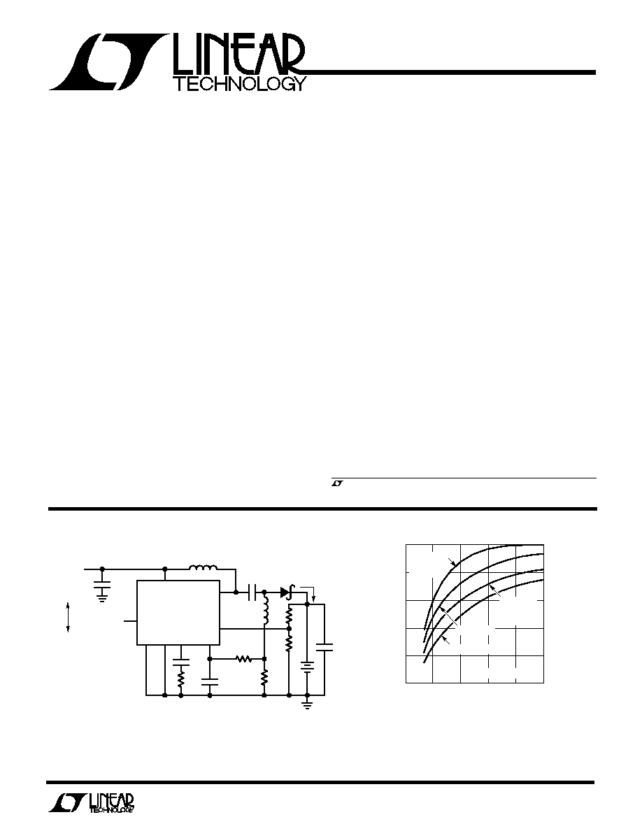
TYPICAL APPLICATIO
N
U
Figure 1. SEPIC Charger with 0.5A Output Current
Maximum Charging Current
ACTUAL PROGRAMMED CHARGING CURRENT WILL BE INDEPENDENT OF
INPUT VOLTAGE AND BATTERY VOLTAGE IF IT DOES NOT EXCEED THE
VALUES SHOWN. THESE ARE ELECTRICAL LIMITATIONS BASED ON MAXIMUM
SWITCH CURRENT. PACKAGE THERMAL LIMITATIONS MAY REDUCE
MAXIMUM CHARGING CURRENT. SEE APPLICATIONS INFORMATION.
INPUT VOLTAGE (V)
0
CURRENT (A)
0.6
0.8
1.0
20
1512 TA02
0.4
0.2
0
5
10
15
25
INDUCTOR = 33
µ
H
DOUBLE
LITHIUM
CELL (8.2V)
6V BATTERY
12V BATTERY
SINGLE
LITHIUM
CELL (4.1V)
LT1512
I
FB
V
C
V
IN
L1 A*
L1 B*
0.5A
·
GND GND S
FB
1512 F01
V
SW
SYNC
AND/OR
SHUTDOWN
WALL
ADAPTER
INPUT
S/S
C3
22
µ
F
25V
C2**
2.2
µ
F
C5
0.1
µ
F
*
**
L1 A, L1 B ARE TWO 33
µ
H WINDINGS ON A
SINGLE INDUCTOR: COILTRONICS CTX33-3
TOKIN CERAMIC 1E225ZY5U-C203-F
C4
0.22
µ
F
R4
24
+
CHARGE
SHUTDOWN
·
R1
R2
R3
0.2
R5
1k
C1
22
µ
F
25V
+
D1
MBRS130LT3
2
LT1512
A
U
G
W
A
W
U
W
A
R
BSOLUTE
XI
TI
S
W
U
U
PACKAGE/ORDER I FOR ATIO
SYMBOL
PARAMETER
CONDITIONS
MIN
TYP
MAX
UNITS
V
REF
V
FB
Reference Voltage
Measured at FB Pin
1.233
1.245
1.257
V
V
C
= 0.8V
q
1.228
1.245
1.262
V
FB Input Current
V
FB
= V
REF
300
550
nA
q
600
nA
FB Reference Voltage Line Regulation
2.7V
V
IN
25V, V
C
= 0.8V
q
0.01
0.03
%/V
V
IREF
I
FB
Reference Voltage
Measured at I
FB
Pin
107
100
93
mV
V
FB
= 0V, V
C
= 0.8V
q
110
100
90
mV
I
FB
Input Current
V
IFB
= V
IREF
(Note 2)
q
10
25
35
µ
A
I
FB
Reference Voltage Line Regulation
2.7V
V
IN
25V, V
C
= 0.8V
q
0.01
0.05
%/V
g
m
Error Amplifier Transconductance
I
C
=
±
25
µ
A
1100
1500
1900
µ
mho
q
700
2300
µ
mho
Error Amplifier Source Current
V
FB
= V
REF
150mV, V
C
= 1.5V
q
120
200
350
µ
A
Error Amplifier Sink Current
V
FB
= V
REF
+ 150mV, V
C
= 1.5V
q
1400
2400
µ
A
Error Amplifier Clamp Voltage
High Clamp, V
FB
= 1V
1.70
1.95
2.30
V
Low Clamp, V
FB
= 1.5V
0.25
0.40
0.52
V
A
V
Error Amplifier Voltage Gain
500
V/ V
V
C
Pin Threshold
Duty Cycle = 0%
0.8
1
1.25
V
f
Switching Frequency
2.7V
V
IN
25V
450
500
550
kHz
0
°
C
T
J
125
°
C
q
430
500
580
kHz
40
°
C
T
J
< 0
°
C (LT1512I)
400
580
kHz
Maximum Switch Duty Cycle
q
88
95
%
Switch Current Limit Blanking Time
130
260
ns
BV
Output Switch Breakdown Voltage
0
°
C
T
J
125
°
C
q
40
47
V
40
°
C
T
J
< 20
°
C (LT1512I)
35
V
V
IN
= 5V, V
C
= 0.6V, V
FB
= V
REF
, I
FB
= 0V, V
SW
and S/S pins open, unless otherwise noted.
ELECTRICAL C
C
HARA TERISTICS
Input Voltage .......................................................... 30V
Switch Voltage ........................................................ 40V
S/S Pin Voltage ....................................................... 30V
FB Pin Voltage (Transient, 10ms) .........................
±
10V
V
FB
Pin Current .................................................... 10mA
I
FB
Pin Voltage (Transient, 10ms) .........................
±
10V
Storage Temperature Range ................ 65
°
C to 150
°
C
Ambient Temperature Range
LT1512C (Note 3) .................................... 0
°
C to 70
°
C
LT1512I .............................................. 40
°
C to 85
°
C
Operating Junction Temperature Range
LT1512C (Note 3) ............................ 20
°
C to 125
°
C
LT1512I ............................................ 40
°
C to 125
°
C
Short Circuit ......................................... 0
°
C to 150
°
C
Lead Temperature (Soldering, 10 sec) ................. 300
°
C
ORDER PART
NUMBER
T
JMAX
= 125
°
C,
JA
= 100
°
C/ W (N)
T
JMAX
= 125
°
C,
JA
= 130
°
C/ W (S)
Consult factory for Military grade parts.
1
2
3
4
8
7
6
5
TOP VIEW
V
C
FB
I
FB
S/S
V
SW
GND
GND S
V
IN
N8 PACKAGE
8-LEAD PDIP
S8 PACKAGE
8-LEAD PLASTIC SO
S8 PART
MARKING
1512
1512I
LT1512CN8
LT1512CS8
LT1512IN8
LT1512IS8
NOTE: CONTACT FACTORY CONCERNING 16-LEAD
FUSED-LEAD GN PACKAGE WITH LOWER THERMAL
RESISTANCE
3
LT1512
SYMBOL
PARAMETER
CONDITIONS
MIN
TYP
MAX
UNITS
V
SAT
Output Switch ON Resistance
I
SW
= 2A
q
0.5
0.8
I
LIM
Switch Current Limit
Duty Cycle = 50%
q
1.5
1.9
2.7
A
Duty Cycle = 80% (Note 1)
q
1.3
1.7
2.5
A
I
IN
Supply Current Increase During Switch ON Time
15
25
mA/A
I
SW
Control Voltage to Switch Current
2
A/V
Transconductance
Minimum Input Voltage
q
2.4
2.7
V
I
Q
Supply Current
2.7V
V
IN
25V
q
4
5.5
mA
Shutdown Supply Current
2.7V
V
IN
25V, V
S/S
0.6V
0
°
C
T
J
125
°
C
q
12
30
µ
A
40
°
C
T
J
0
°
C (LT1512I)
50
µ
A
Shutdown Threshold
2.7V
V
IN
25V
q
0.6
1.3
2
V
Shutdown Delay
q
5
12
25
µ
s
S/S Pin Input Current
0V
V
S/S
5V
q
10
15
µ
A
Synchronization Frequency Range
q
600
800
kHz
ELECTRICAL C
C
HARA TERISTICS
V
IN
= 5V, V
C
= 0.6V, V
FB
= V
REF
, I
FB
= 0V, V
SW
and S/S pins open, unless otherwise noted.
The
q
denotes specifications which apply over the full operating
temperature range.
Note 1: For duty cycles (DC) between 50% and 85%, minimum
guaranteed switch current is given by I
LIM
= 0.667 (2.75 DC).
Note 2: The I
FB
pin is servoed to its regulating state with V
C
= 0.8V.
Note 3: Commercial devices are guaranteed over 0
°
C to 125
°
C junction
temperature range and 0
°
C to 70
°
C ambient temperature range. These
parts are also designed, characterized and expected to operate over the
20
°
C to 85
°
C extended ambient temperature range, but are not tested at
20
°
C or 85
°
C. Devices with full guaranteed electrical specifications over
the ambient temperature range 40
°
C to 85
°
C are available as industrial
parts with an "I" suffix.
Maximum allowable ambient temperature may be limited by power
dissipation. Parts may not necessarily be operated simultaneously at
maximum power dissipation and maximum ambient temperature.
Temperature rise calculations must be done as shown in the Applications
Information section to ensure that maximum junction temperature does
not exceed 125
°
C limit. With high power dissipation, maximum ambient
temperature may be less than 70
°
C.
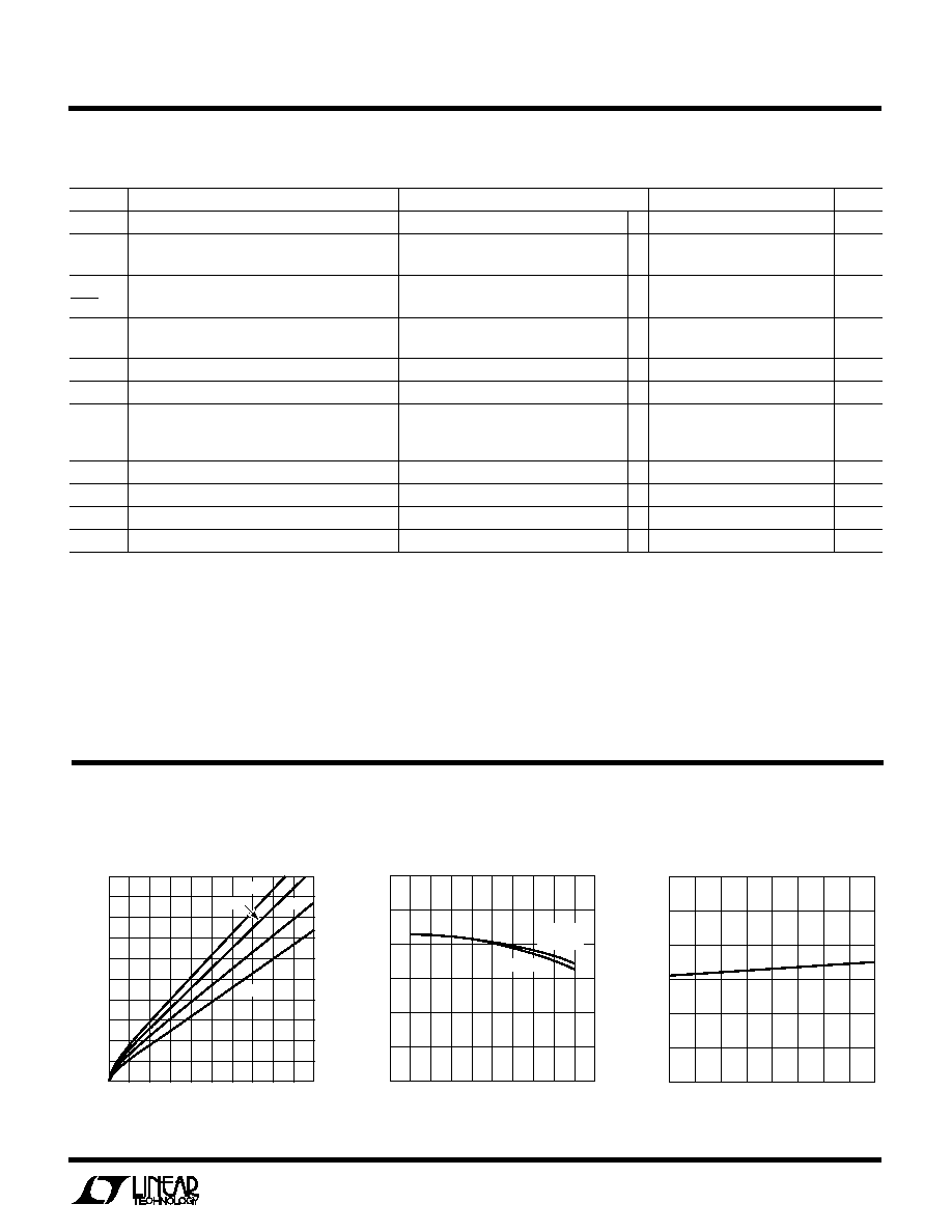
TYPICAL PERFOR
M
A
N
CE CHARACTERISTICS
U
W
Switch Saturation Voltage
vs Switch Current
Minimum Input Voltage
vs Temperature
Switch Current Limit
vs Duty Cycle
SWITCH CURRENT (A)
0
SWITCH SATURATION VOLTAGE (V)
0.6
0.8
1.0
1.6
1512 G01
0.4
0.2
0.5
0.7
0.9
0.3
0.1
0
0.4
0.8
1.2
2.0
1.4
0.2
0.6
1.0
1.8
100
°
C
150
°
C
25
°
C
55
°
C
DUTY CYCLE (%)
SWITCH CURRENT LIMIT (A)
3.0
2.5
2.0
1.5
1.0
0.5
0
20
40
60
80
1512 G02
100
10
0
30
50
70
90
25
°
C AND
125
°
C
55
°
C
TEMPERATURE (
°
C)
50
1.8
INPUT VOLTAGE (V)
2.0
2.2
2.4
2.6
0
50
100
150
1512 G03
2.8
3.0
25
25
75
125
4
LT1512
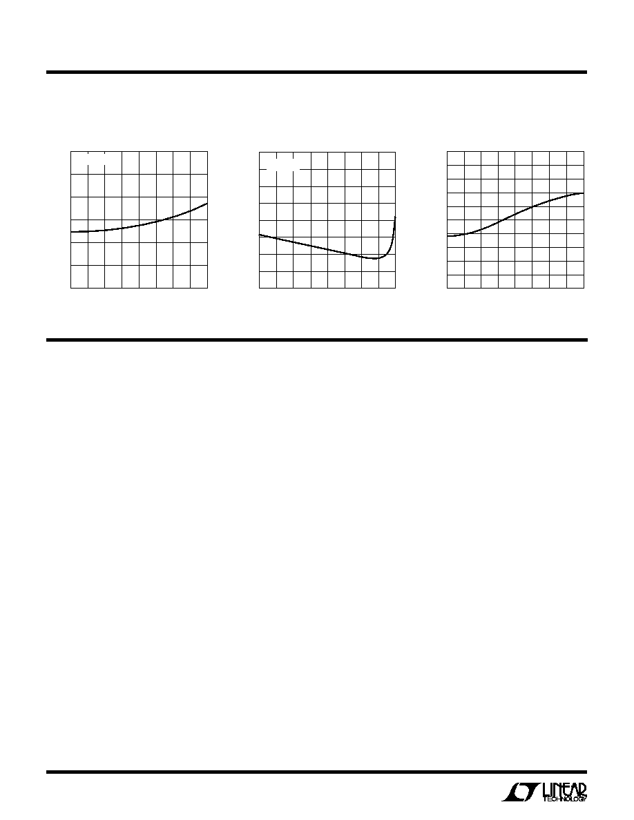
TYPICAL PERFOR
M
A
N
CE CHARACTERISTICS
U
W
Minimum Peak-to-Peak
Synchronization Voltage vs Temp
Feedback Input Current
vs Temperature
Negative Feedback Input Current
vs Temperature
TEMPERATURE (
°
C)
50
0
MINIMUM SYNCHRONIZATION VOLTAGE (V
P-P
)
0.5
1.0
1.5
2.0
0
50
100
150
1512 G04
2.5
3.0
25
25
75
125
f
SYNC
= 700kHz
TEMPERATURE (
°
C)
50
FEEDBACK INPUT CURRENT (nA)
400
500
600
150
1512 G05
300
200
0
0
50
100
100
800
700
25
25
75
125
V
FB
= V
REF
TEMPERATURE (
°
C)
50
50
NEGATIVE FEEDBACK INPUT CURRENT (
µ
A)
30
0
0
50
75
1512 G06
40
10
20
25
25
100 125
150
PI
N
FU
N
CTIO
N
S
U
U
U
V
C
: The compensation pin is primarily used for frequency
compensation, but it can also be used for soft starting and
current limiting. It is the output of the error amplifier and
the input of the current comparator. Peak switch current
increases from 0A to 1.8A as the V
C
voltage varies from 1V
to 1.9V. Current out of the V
C
pin is about 200
µ
A when the
pin is externally clamped below the internal 1.9V clamp
level. Loop frequency compensation is performed with a
capacitor or series RC network from the V
C
pin
directly to
the ground pin (avoid ground loops).
FB: The feedback pin is used for positive output voltage
sensing. This pin is the inverting input to the voltage error
amplifier. The R1/R2 voltage divider connected to FB
defines Li-Ion float voltage at full charge, or acts as a
voltage limiter for NiCd or NiMH applications. Input bias
current is typically 300nA, so divider current is normally
set to 100
µ
A to swamp out any output voltage errors due
to bias current. The noninverting input of this amplifier is
tied internally to a 1.245V reference. The grounded end of
the output voltage divider should be connected directly to
the LT1512 ground pin (avoid ground loops).
I
FB
: The current feedback pin is used to sense charging
current. It is the input to a current sense amplifier that
controls charging current when the battery voltage is
below the programmed voltage. During constant-current
operation, the I
FB
pin regulates at 100mV. Input resis-
tance of this pin is 5k
, so filter resistance (R4, Figure 1)
should be less than 50
. The 24
, 0.22
µ
F filter shown in
Figure 1 is used to convert the pulsating current in the
sense resistor to a smooth DC current feedback signal.
S/S: This pin can be used for shutdown and/or synchroni-
zation. It is logic level compatible, but can be tied to V
IN
if
desired. It defaults to a high ON state when floated. A logic
low state will shut down the charger to a micropower state.
Driving the S/S pin with a continuous logic signal of
600kHz to 800kHz will synchronize switching frequency to
the external signal. Shutdown is avoided in this mode with
an internal timer.
V
IN
: The input supply pin should be bypassed with a low
ESR capacitor located right next to the IC chip. The
grounded end of the capacitor must be connected directly
to the ground plane to which the GND pin is connected.
GND S, GND: The LT1512 uses separate ground pins for
switch current (GND) and the control circuitry (GND S).
This isolates the control ground from any induced voltage
created by fast switch currents. Both pins should be tied
directly to the ground plane, but the external control
circuit components such as the voltage divider, frequency
compensation network and I
FB
bypass capacitor should
5
LT1512
PI
N
FU
N
CTIO
N
S
U
U
U
be connected directly to the GND S pin or to the ground
plane close to the point where the GND S pin is connected.
V
SW
: The switch pin is the collector of the power switch,
carrying up to 1.5A of current with fast rise and fall times.
Keep the traces on this pin as short as possible to minimize
radiation and voltage spikes. In particular, the path in
Figure 1 which includes SW to C2, D1, C1 and around to
the LT1512 ground pin should be as short as possible to
minimize voltage spikes at switch turn-off.
+
I
FBA
I
FB
S/S
FB
5k
62k
0.08
+
EA
V
C
V
IN
GND
1512 F02
GND S
1.245V
REF
500kHz
OSC
SYNC
SHUTDOWN
DELAY AND RESET
LOW DROPOUT
2.3V REG
ANTI-SAT
LOGIC
DRIVER
SW
SWITCH
+
IA
A
V
6
COMP
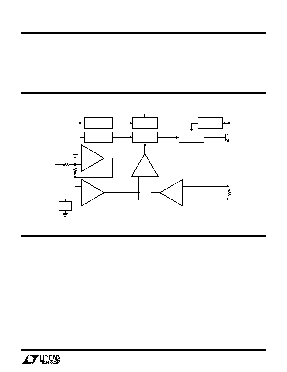
Figure 2
BLOCK DIAGRA
M
W
OPERATIO
N
U
The LT1512 is a current mode switcher. This means that
switch duty cycle is directly controlled by switch current
rather than by output voltage or current. Referring to the
Block Diagram, the switch is turned "on" at the start of each
oscillator cycle. It is turned "off" when switch current
reaches a predetermined level. Control of output voltage
and current is obtained by using the output of a dual
feedback voltage sensing error amplifier to set switch
current trip level. This technique has the advantage of
simplified loop frequency compensation. A low dropout
internal regulator provides a 2.3V supply for all internal
circuitry on the LT1512. This low dropout design allows
input voltage to vary from 2.7V to 25V. A 500kHz oscillator
is the basic clock for all internal timing. It turns "on" the
output switch via the logic and driver circuitry. Special
adaptive antisat circuitry detects onset of saturation in the
power switch and adjusts driver current instantaneously to
limit switch saturation. This minimizes driver dissipation
and provides very rapid turn-off of the switch.
A unique error amplifier design has two inverting inputs
which allow for sensing both output voltage and current. A
1.245V bandgap reference biases the noninverting input.
The first inverting input of the error amplifier is brought out
for positive output voltage sensing. The second inverting
input is driven by a "current" amplifier which is sensing
output current via an external current sense resistor. The