1528f.pm6
1
LT1528
1528fa
s
Dropout Voltage: 0.6V at I
OUT
= 3A
s
Fast Transient Response
s
Output Current: 3A
s
Quiescent Current: 400
µ
A
s
No Protection Diodes Needed
s
Fixed Output Voltage: 3.3V
s
Controlled Quiescent Current in Dropout
s
Shutdown I
Q
= 125
µ
A
s
Stable with 3.3
µ
F Output Capacitor
s
Reverse Battery Protection
s
No Reverse Output Current
s
Thermal Limiting
The LT
®
1528 is a 3A low dropout regulator optimized to
handle the large load current transients associated with
the current generation of microprocessors. This device
has the fastest transient response of currently available
PNP regulators and is very tolerant of variations in capaci-
tor ESR. Dropout voltage is 75mV at 10mA, rising to
300mV at 1A and 600mV at 3A. The device has a quiescent
current of 400
µ
A. Quiescent current is well controlled; it
does not increase significantly as the device enters drop-
out. The regulator can operate with output capacitors as
small as 3.3
µ
F, although larger capacitors will be needed
to achieve the performance required in most microproces-
sor applications. The LT1528 is available with a fixed
output voltage of 3.3V. An external SENSE pin allows
adjustment to output voltages greater than 3.3V, using a
simple resistive divider. This allows the device to be
adjusted over a wide range of output voltages, including
the 3.3V to 4.2V range required by a variety of processors
from Intel, IBM, AMD, and Cyrix.
The LT1528 has both reverse input and reverse output
protection and includes a shutdown feature. Quiescent
current drops to 125
µ
A in shutdown. The LT1528 is
available in 5-lead TO-220 and 5-lead DD packages.
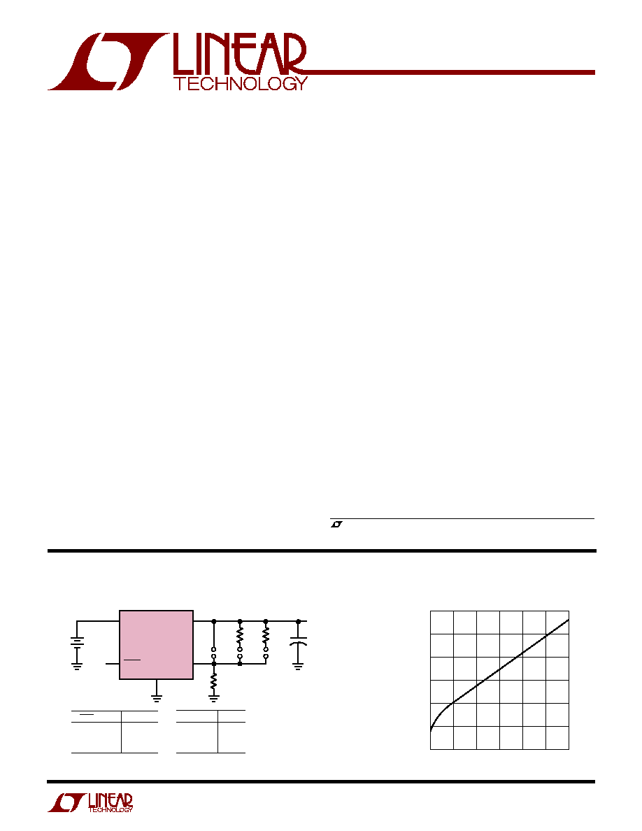
3A Low Dropout Regulator
for Microprocessor Applications
Microprocessor Supply with Shutdown
OUTPUT CURRENT (mA)
0
0
DROPOUT VOLTAGE (V)
0.1
0.2
0.3
0.4
0.6
0.5
1.0
1.5
2.0
LT1528 · TA02
2.5
3.0
0.5
Dropout Voltage
, LTC and LT are registered trademarks of Linear Technology Corporation.
s
Microprocessor Applications
s
Post Regulator for Switching Supplies
s
5V to 3.3V Logic Regulator
5
4
1
2
3
+
V
IN
=5V
4
×
47
µ
F*
SOLID TANTALUM
V
OUT
V
SHDN
(PIN 4)
OUTPUT
<0.25 OFF
>2.80 ON
NC ON
SHORTING
V
OUT
J1 3.30
J2
3.45
J3
4.00
LT1528 · TA01
GND
IN
SHDN
OUT
SENSE
J1
J2
J3
15
68
330
LT1528
*CHOOSE CAPACITORS
TO MEET PROCESSOR
REQUIREMENTS
DESCRIPTIO
U
FEATURES
APPLICATIO S
U
TYPICAL APPLICATIO
U
2
LT1528
1528fa
Output Short-Circuit Duration .......................... Indefinite
Storage Temperature Range ................. 65
°
C to 150
°
C
Operating Junction Temperature Range
LT1528C ............................................... 0
°
C to 125
°
C
Lead Temperature (Soldering, 10 sec).................. 300
°
C
*For applications requiring input voltage ratings greater than 15V, contact
the factory.
ORDER PART
NUMBER
LT1528CT
ORDER PART
NUMBER
LT1528CQ
T
JMAX
= 125
°
C,
JA
= 30
°
C/ W
Input Voltage .......................................................
±
15V*
OUTPUT Pin Reverse Current ............................... 10mA
SENSE Pin Current ............................................... 10mA
SHDN Pin Input Voltage (Note 2) ................ 6.5V, 0.3V
SHDN Pin Input Current (Note 2) ........................... 5mA
PARAMETER
CONDITIONS
MIN
TYP
MAX
UNITS
Regulated Output Voltages (Notes 3, 4)
V
IN
= 3.8V, I
OUT
= 1mA
3.250
3.300
3.350
V
4.3V < V
IN
< 15V, 1mA < I
OUT
< 3A
q
3.200
3.300
3.400
V
Line Regulation (Note 4)
V
IN
= 3.8V to 15V, I
OUT
= 1mA
q
1.5
10
mV
Load Regulation (Note 4)
I
LOAD
= 1mA to 3A, V
IN
= 4.3V
12
20
mV
I
LOAD
= 1mA to 3A, V
IN
= 4.3V
q
15
30
mV
Dropout Voltage (Note 5)
I
LOAD
= 10mA
70
110
mV
I
LOAD
= 10mA
q
150
mV
I
LOAD
= 100mA
150
200
mV
I
LOAD
= 100mA
q
250
mV
I
LOAD
= 700mA
280
320
mV
I
LOAD
= 700mA
q
420
mV
I
LOAD
= 1.5A
390
450
mV
I
LOAD
= 1.5A
q
600
mV
I
LOAD
= 3A
570
670
mV
I
LOAD
= 3A
q
850
mV
T
JMAX
= 125
°
C,
JA
= 50
°
C/ W
(Note 1)
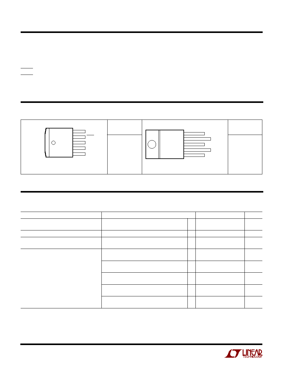
Q PACKAGE
5-LEAD PLASTIC DD
FRONT VIEW
TAB IS
GND
V
IN
SHDN
GND
SENSE
OUTPUT
5
4
3
2
1
T PACKAGE
5-LEAD PLASTIC TO-220
V
IN
SHDN
GND
SENSE
OUTPUT
FRONT VIEW
TAB IS
GND
5
4
3
2
1
ABSOLUTE AXI U RATI GS
W
W
W
U
PACKAGE/ORDER I FOR ATIO
U
U
W
Consult LTC Marketing for parts specified with wider operating temperature ranges.
ELECTRICAL CHARACTERISTICS
The
q
denotes the specifications which apply over the full operating temperature range, otherwise specifications are at T
J
= 25
°
C.
3
LT1528
1528fa
PARAMETER
CONDITIONS
MIN
TYP
MAX
UNITS
GND Pin Current (Note 6)
I
LOAD
= 0mA
450
750
µ
A
I
LOAD
= 0mA, T
J
= 125
°
C (Note 7)
1.9
mA
I
LOAD
= 100mA
1.2
2.5
mA
I
LOAD
= 100mA, T
J
= 125
°
C (Note 7)
2.7
mA
I
LOAD
= 300mA
2.6
4.0
mA
I
LOAD
= 300mA, T
J
= 125
°
C (Note 7)
4.1
mA
I
LOAD
= 700mA
7.3
12.0
mA
I
LOAD
= 700mA, T
J
= 125
°
C (Note 7)
8.8
mA
I
LOAD
= 1.5A
q
22
40
mA
I
LOAD
= 3A
q
85
140
mA
SENSE Pin Current (Notes 4, 8)
90
130
250
µ
A
SHDN Threshold
V
OUT
= Off-to-On
q
1.20
2.80
V
V
OUT
= On-to-Off
q
0.25
0.75
V
SHDN Pin Current (Note 9)
V
SHDN
= 0V
q
37
100
µ
A
Quiescent Current in Shutdown (Note 10)
V
IN
= 6V, V
SHDN
= 0V
q
110
220
µ
A
Ripple Rejection
V
IN
V
OUT
= 1V(Avg), V
RIPPLE
= 0.5V
P-P
,
50
67
dB
f
RIPPLE
= 120Hz, I
LOAD
= 1.5A
Current Limit
V
IN
V
OUT
= 7V
4.5
A
V
IN
= 4.3V,
V
OUT
= 0.1V
q
3.2
4.0
A
Input Reverse Leakage Current
V
IN
= 15V, V
OUT
= 0V
q
1.0
mA
Reverse Output Current (Note 11)
V
OUT
= 3.3V, V
IN
= 0V
120
250
µ
A
Note 1: Absolute Maximum Ratings are those values beyond which the life
of a device may be impaired.
Note 2: The SHDN pin input voltage rating is required for a low impedance
source. Internal protection devices connected to the SHDN pin will turn on
and clamp the pin to approximately 7V or 0.6V. This range allows the use
of 5V logic devices to drive the pin directly. For high impedance sources or
logic running on supply voltages greater than 5.5V, the maximum current
driven into the SHDN pin must be less than 5mA.
Note 3: Operating conditions are limited by maximum junction
temperature. The regulated output voltage specification will not apply for
all possible combinations of input voltage and output current. When
operating at maximum input voltage, the output current must be limited.
When operating at maximum output current, the input voltage range
must be limited.
Note 4: The LT1528 is tested and specified with the SENSE pin connected
to the OUTPUT pin.
Note 5: Dropout voltage is the minimum input/output voltage required to
maintain regulation at the specified output current. In dropout the output
voltage will be equal to: (V
IN
V
DROPOUT
).
Note 6: GND pin current is tested with V
IN
= V
OUT
(nominal) and a current
source load. This means that the device is tested while operating in its
dropout region. This is the worst-case GND pin current. The GND pin
current will decrease slightly at higher input voltages.
Note 7: GND pin current will rise at T
J
> 75
°
C. This is due to internal
circuitry designed to compensate for leakage currents in the output
transistor at high temperatures. This allows quiescent current to be
minimized at lower temperatures, yet maintain output regulation at high
temperatures with light loads. See quiescent current curve in typical
performance characteristics section.
Note 8: SENSE pin current flows into the SENSE pin.
Note 9: SHDN pin current at V
SHDN
= 0V flows out of the SHDN pin.
Note 10: Quiescent current in shutdown is equal to the total sum of the
SHDN pin current (40
µ
A) and the GND pin current (70
µ
A).
Note 11: Reverse output current is tested with the input pin grounded and
the OUTPUT pin forced to the rated output voltage. This current flows into
the OUTPUT pin and out of the GND pin.
The
q
denotes the specifications which apply over the full operating temperature range, otherwise specifications are at T
J
= 25
°
C.
ELECTRICAL CHARACTERISTICS
4
LT1528
1528fa
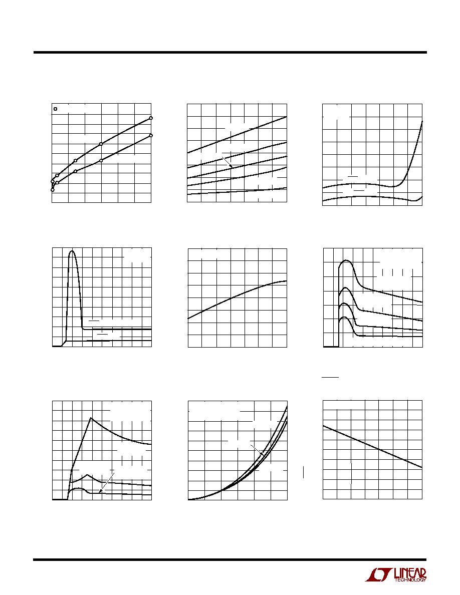
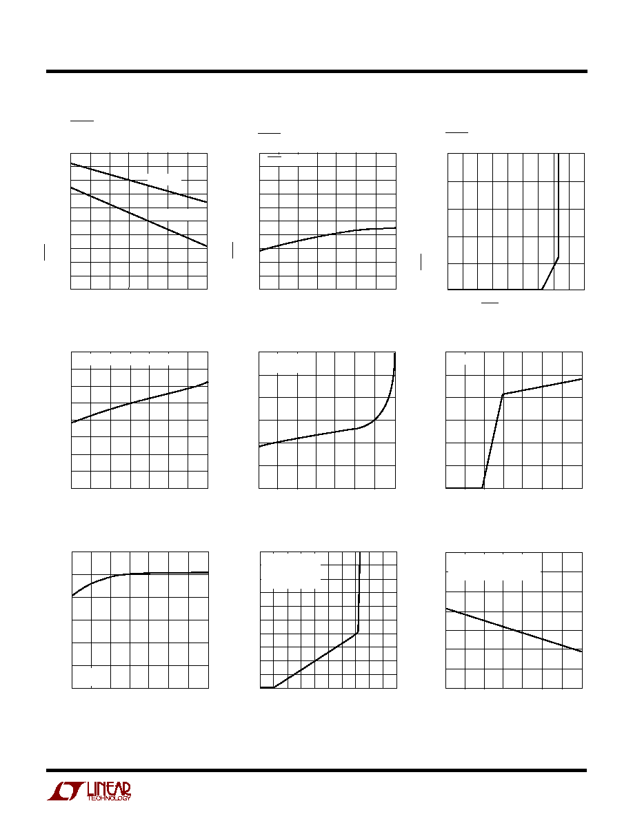
Quiescent Current
Dropout Voltage
Guaranteed Dropout Voltage
TEMPERATURE (
°
C)
50
DROPOUT VOLTAGE (V)
25
LT1528 · TPC02
25
0
50
0.8
0.7
0.6
0.5
0.4
0.3
0.2
0.1
0
75
100
125
I
LOAD
= 3A
I
LOAD
= 1.5A
I
LOAD
= 300mA
I
LOAD
= 10mA
I
LOAD
= 700mA
TEMPERATURE (
°
C)
50
QUIESCENT CURRENT (mA)
25
LT1528 · TPC03
25
0
50
2.00
1.75
1.50
1.25
1.00
0.75
0.50
0.25
0
75
100
125
V
SHDN
= OPEN
V
SHDN
= 0V
V
IN
= 4.3V
R
L
=
SENSE Pin Voltage
GND Pin Current
Quiescent Current
INPUT VOLTAGE (V)
0
QUIESCENT CURRENT (
µ
A)
2000
1750
1500
1250
1000
750
500
250
0
8
LT1528 · TPC04
2
1
3
5
7
9
4
6
10
I
LOAD
= 0
R
LOAD
=
V
SHDN
= OPEN (HIGH)
V
SHDN
= 0V
TEMPERATURE (
°
C)
50
SENSE PIN VOLTAGE (V)
25
LT1528 · TPC05
25
0
50
3.400
3.375
3.350
3.325
3.300
3.275
3.250
3.225
3.200
75
100
125
I
LOAD
= 1mA
SHDN Pin Threshold
(On-to-Off)
GND Pin Current
GND Pin Current
INPUT VOLTAGE (V)
0
GND PIN CURRENT (mA)
100
90
80
70
60
50
40
30
20
10
0
8
LT1528 · TPC07
2
1
3
5
7
9
4
6
10
T
J
= 25
°
C
V
OUT
= V
SENSE
*FOR V
OUT
= 3.3V
R
L
= 1.1
I
LOAD
= 3A*
R
L
= 2.2
I
LOAD
= 1.5A*
R
L
= 4.7
I
LOAD
= 700mA*
OUTPUT CURRENT (A)
0
DROPOUT VOLTAGE (V)
0.5
1.0
1.5
2.0
LT1528 · TPC01
2.5
1.0
0.9
0.8
0.7
0.6
0.5
0.4
0.3
0.2
0.1
0
3.0
T
J
125
°
C
T
J
25
°
C
= TEST POINTS
OUTPUT CURRENT (A)
0
GND PIN CURRENT (mA)
0.5
1.0
1.5
2.0
LT1528 · TPC08
2.5
100
90
80
70
60
50
40
30
20
10
0
3.0
T
J
= 125
°
C
T
J
= 50
°
C
T
J
= 25
°
C
V
IN
= 3.3V
DEVICE IS OPERATING
IN DROPOUT
INPUT VOLTAGE (V)
0
0
GND PIN CURRENT (mA)
1
3
4
5
7
1
5
7
LT1528 · TPC06
2
6
4
9
10
2
3
6
8
R
L
= 6.6
I
LOAD
= 500mA*
R
L
= 11
I
LOAD
= 300mA*
R
L
= 33
I
LOAD
= 100mA*
R
L
= 330
: I
LOAD
= 10mA*
T
J
= 25
°
C
V
OUT
= V
SENSE
*FOR V
OUT
= 3.3V
TEMPERATURE (
°
C)
50
SHDN PIN THRESHOLD (V)
2.0
1.8
1.6
1.4
1.2
1.0
0.8
0.6
0.4
0.2
0
0
50
75
LT1528 · TPC09
25
25
100
125
I
LOAD
= 1mA
TYPICAL PERFOR A CE CHARACTERISTICS
U
W
5
LT1528
1528fa
SHDN Pin Current
Current Limit
Reverse Output Current
SHDN Pin Input Current
TEMPERATURE (
°
C)
50
SHDN PIN THRESHOLD (V)
2.0
1.8
1.6
1.4
1.2
1.0
0.8
0.6
0.4
0.2
0
0
50
75
LT1528 · TPC10
25
25
100
125
I
LOAD
= 3A
I
LOAD
= 1mA
TEMPERATURE (
°
C)
50
SHDN PIN CURRENT (
µ
A)
100
90
80
70
60
50
40
30
20
10
0
0
50
75
LT1528 · TPC11
25
25
100
125
V
SHDN
= 0V
SHDN PIN VOLTAGE (V)
0
0
SHDN PIN INPUT CURRENT (mA)
5
15
20
25
2
4
5
9
LT1528 · TPC12
10
1
3
6
7
8
SENSE Pin Current
TEMPERATURE (
°
C)
50
SENSE PIN CURRENT (
µ
A)
25
LT1528 · TPC13
25
0
50
200
175
150
125
100
75
50
25
0
75
100
125
CURRENT FLOWS INTO SENSE PIN
TEMPERATURE (
°
C)
50
OUTPUT CURRENT (
µ
A)
300
250
200
150
100
50
0
25
75
LT1528 · TPC14
25
0
50
100
125
V
IN
= 0V
V
OUT
= V
SENSE
INPUT VOLTAGE (V)
0
SHORT-CIRCUIT CURRENT (A)
6
5
4
3
2
1
0
3
5
LT1528 · TPC15
1
2
4
6
7
V
OUT
= 0V
Reverse Output Current
Current Limit
Ripple Rejection
TEMPERATURE (
°
C)
50
SHORT-CIRCUIT CURRENT (A)
6
5
4
3
2
1
0
25
75
LT1528 · TPC16
25
0
50
100
125
V
IN
= 7V
V
OUT
= 0V
OUTPUT VOLTAGE (V)
0
OUTPUT CURRENT (
µ
A)
1000
900
800
700
600
500
400
300
200
100
0
8
LT1528 · TPC17
2
1
3
5
7
9
4
6
10
T
J
= 25
°
C, V
IN
= 0V
V
OUT
=V
SENSE
CURRENT FLOWS
INTO DEVICE
TEMPERATURE (
°
C)
50
64
66
70
25
75
LT
1528 · TPC18
62
60
25
0
50
100
125
58
56
68
RIPPLE REJECITON (dB)
V
IN(AVG)
= 4.3V
V
RIPPLE
= 0.5V
P-P
AT f = 120Hz
I
L
= 1.5A
SHDN Pin Threshold
(Off-to-On)
TYPICAL PERFOR A CE CHARACTERISTICS
U
W