 | ÐлекÑÑоннÑй компоненÑ: LT1533IS | СкаÑаÑÑ:  PDF PDF  ZIP ZIP |
Äîêóìåíòàöèÿ è îïèñàíèÿ www.docs.chipfind.ru
1
LT1533
Ultralow Noise
1A Switching Regulator
FEATURES
DESCRIPTIO
N
U
The LT
®
1533 is a new class of switching regulator designed
to reduce conducted and radiated electromagnetic interfer-
ence (EMI). Ultralow noise and EMI are achieved by providing
user control of the output switch slew rates. Voltage and
current slew rates can be independently programmed to
optimize switcher harmonic content versus efficiency. The
LT1533 can reduce high frequency harmonic power by as
much as 40dB with only minor losses in efficiency.
The LT1533 utilizes a dual output switch current mode
architecture optimized for low noise topologies. The IC
includes two 1A power switches along with all necessary
oscillator, control and protection circuitry. Unique error amp
circuitry can regulate both positive and negative voltages.
The internal oscillator may be synchronized to an external
clock for more accurate placement of switching harmonics.
Protection features include cycle by cycle current limit pro-
tection, undervoltage lockout and thermal shutdown.
Low minimum supply voltage and low supply current during
shutdown make the LT1533 well suited for portable applica-
tions. The part may also be forced into a 50% duty cycle mode
for unregulated applications. The LT1533 is available in the
16-pin narrow SO package.
s
Greatly Reduced Conducted and Radiated EMI
(<100
µ
V
P-P
in Typical Application)
s
Low Switching Harmonic Content
s
Independent Control of Switch Voltage and
Current Slew Rates
s
Two 1A Current Limited Power Switches
s
Regulates Positive and Negative Voltages
s
20kHz to 250kHz Oscillator Frequency
s
Easily Synchronized to External Clock
s
Wide Input Voltage Range: 2.7V to 23V
s
Low Shutdown Current: 12
µ
A Typical
s
Easier Layout than with Conventional Switchers
s
Outputs Can Be Forced to 50% Duty Cycle for
Unregulated Applications
s
Precision Instrumentation Systems
s
Isolated Supplies for Industrial Automation
s
Medical Instruments
s
Wireless Communications
s
Single Board Data Acquisition Systems
APPLICATIO
N
S
U
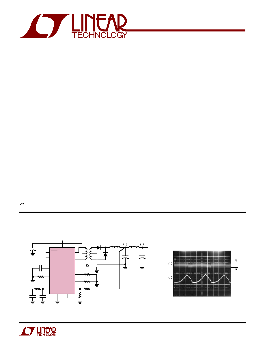
TYPICAL APPLICATIO
N
U
, LTC and LT are registered trademarks of Linear Technology Corporation.
SHDN
DUTY
SYNC
COL A
COL B
PGND
R
VSL
R
CSL
FB
NFB
LT1533
GND
V
IN
5V
14
2
15
16
13
12
7
11
3
4
5
6
10
820pF
16.9k
0.015
µ
F
1000pF
15k
Note 1
33
µ
F
15k
15k
+
T1
1N4148
B
A
L1
300
µ
H
L2
33
µ
H
1N4148
2.49k
1%
8
9
21.5k, 1%
C1
47
µ
F
16V
+
C2
33
µ
F
20V
C1: SANYO OS-CON
C2: AVX TPS TANTALUM
L1: COILTRONICS CTX300-2
L2: COILCRAFT DT1608C-333
T1: COILTRONICS CTX02-13834
NOTE 1: 25nH TRACE INDUCTANCE
OR COILCRAFT B07T
12V
150mA
1533 TA01
+
C
T
R
T
V
C
Low Noise 5V to 12V Forward Push-Pull DC/DC Converter
B
2mV/DIV
A
100
µ
V/DIV
2
µ
s/DIV
1533 TA02
12V Output Noise (BW = 100MHz)
<100
µ
V
P-P
2
LT1533
ABSOLUTE
M
AXI
M
U
M
RATINGS
W
W
W
U
(Note 1)
Input Voltage (V
IN
) .................................................. 30V
Switch Voltage (COL A, COL B) ............................... 30V
SHDN Pin Voltage .................................................... 30V
Feedback Pin Current ............................................ 10mA
Negative Feedback Pin Current ............................
±
10mA
Storage Temperature Range ................. 65
°
C to 150
°
C
Maximum Junction Temperature ......................... 125
°
C
Operating Junction Temperature Range
LT1533C ............................................... 0
°
C to 100
°
C
LT1533I ............................................ 40
°
C to 100
°
C
Lead Temperature (Soldering, 10 sec).................. 300
°
C
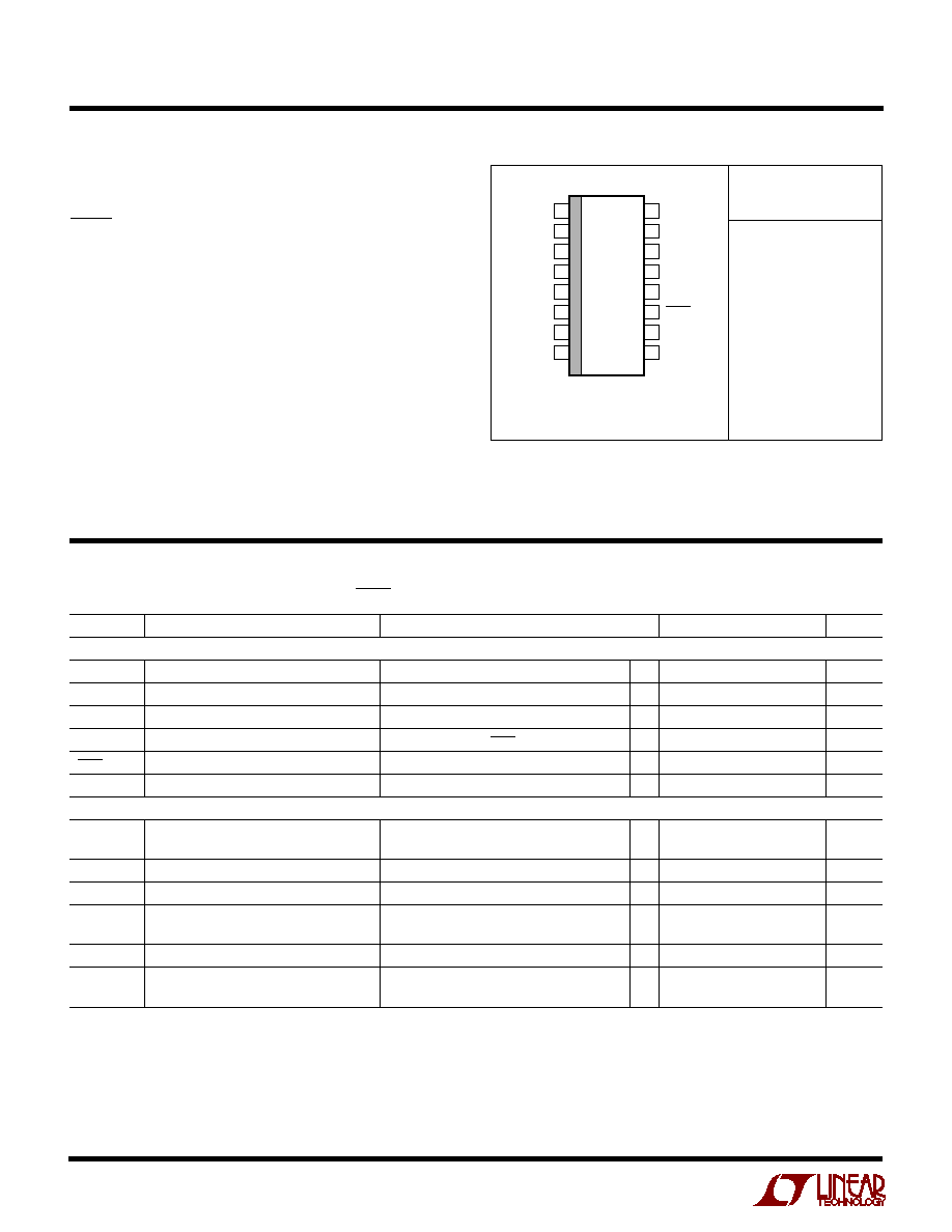
ORDER PART
NUMBER
LT1533CS
LT1533IS
PACKAGE/ORDER I
N
FOR
M
ATIO
N
W
U
U
ELECTRICAL CHARACTERISTICS
V
IN
= 5V, V
C
= 0.9V, V
FB
= V
REF
. COL A, COL B, SHDN, NFB, DUTY pins open, unless otherwise noted.
Consult factory for Military grade parts.
TOP VIEW
S PACKAGE
16-LEAD NARROW PLASTIC SO
1
2
3
4
5
6
7
8
16
15
14
13
12
11
10
9
NC
COL A
DUTY
SYNC
C
T
R
T
FB
NFB
PGND
COL B
V
IN
R
VSL
R
CSL
SHDN
V
C
GND
T
JMAX
= 125
°
C,
JA
= 100
°
C/ W
SYMBOL
PARAMETER
CONDITIONS
MIN
TYP
MAX
UNITS
Supply and Protection
V
IN
Recommended Operating Range
q
2.7
23
V
V
IN(MIN)
Minimum Input Voltage
q
2.55
2.7
V
I
VIN
Supply Current
2.7V
V
IN
23V, R
VSL
, R
CSL
, R
T
= 17k
q
12
18
mA
I
VIN(OFF)
Shutdown Supply Current
2.7V
V
IN
23V, V
SHDN
= 0V
q
12
30
µ
A
V
SHDN
Shutdown Threshold
2.7V
V
IN
23V
q
0.4
0.8
1.2
V
I
SHDN
Shutdown Input Current
2
µ
A
Error Amplifiers
V
REF
Reference Voltage
Measured at Feedback Pin
1.235
1.250
1.265
V
q
1.215
1.250
1.275
V
I
FB
Feedback Input Current
V
FB
= V
REF
q
250
900
nA
FB
REG
Reference Voltage Line Regulation
2.7V
V
IN
23V
q
0.003
0.03
%/V
V
NFR
Negative Feedback Reference Voltage
Measured at Negative Feedback Pin with
q
2.550
2.500
2.420
V
Feedback Pin Open
I
NFR
Negative Feedback Input Current
V
NFB
= V
NFR
q
37
25
µ
A
NFB
REG
Negative Feedback Reference Voltage
2.7V
V
IN
23V
q
0.002
0.05
%/V
Line Regulation
3
LT1533
ELECTRICAL CHARACTERISTICS
V
IN
= 5V, V
C
= 0.9V, V
FB
= V
REF
. COL A, COL B, SHDN, NFB, DUTY pins open, unless otherwise noted.
SYMBOL
PARAMETER
CONDITIONS
MIN
TYP
MAX
UNITS
g
m
Error Amplifier Transconductance
I
C
=
±
25
µ
A
1100
1500
1900
µ
mho
q
700
2300
µ
mho
I
ESK
Error Amplifier Sink Current
V
FB
= V
REF
+ 150mV, V
C
= 0.9V, V
SHDN
= 1V
q
120
200
350
µ
A
I
ESRC
Error Amplifier Source Current
V
FB
= V
REF
150mV, V
C
= 0.9V, V
SHDN
= 1V
q
120
200
350
µ
A
V
CLH
Error Amplifier Clamp Voltage
High Clamp, V
FB
= 1V
1.33
V
V
CLL
Error Amplifier Clamp Voltage
Low Clamp, V
FB
= 1.5V
0.1
V
A
V
Error Amplifier Voltage Gain
180
250
V/V
Oscillator and Sync
f
MAX
Maximum Switch Frequency
250
kHz
f
SYNC
Synchronization Frequency Range
f
OSC
= 250kHz
q
375
kHz
R
SYNC
SYNC Pin Input Resistance
40
k
V
FBfs
FB Pin Threshold for Frequency Shift
5% Reduction from Nominal
0.4
V
Output Switches
DC
MAX
Maximum Switch Duty Cycle
DUTY Pin Open, R
VSL
= R
CSL
= 4.9k, f
OSC
= 25kHz
q
44
45.5
%
DUTY Pin Grounded, Forced 50% Duty Cycle
50.0
%
t
IBL
Switch Current Limit Blanking Time
200
ns
BV
Output Switch Breakdown Voltage
2.7V
V
IN
23V
q
25
30
V
R
ON
Output Switch-On Resistance
I
COL A
or I
COL B
= 0.75A
q
0.5
0.85
I
LIM(MAX)
Maximum Current Limit
Duty Cycle = 15%
1
1.25
1.8
A
Short-Circuit Current Limit
Duty Cycle = 40%
0.8
A
I
IN
/
I
SW
Supply Current Increase During
16
mA/A
Switch-On Time
V
DUTYTH
DUTY Pin Threshold
0.35
Slew Control
V
SLEWR
Output Voltage Slew Rising Edge
Either A or B, R
VSL
, R
CSL
= 17k
11
V/
µ
s
V
SLEWF
Output Voltage Slew Falling Edge
Either A or B, R
VSL
, R
CSL
= 17k
14.5
V/
µ
s
I
SLEWR
Output Current Slew Rising Edge
Either A or B, R
VSL
, R
CSL
= 17k
1.3
A/
µ
s
I
SLEWF
Output Current Slew Falling Edge
Either A or B, R
VSL
, R
CSL
= 17k
1.3
A/
µ
s
The
q
denotes specifications that apply over the full operating
temperature range.
Note 1: Absolute Maximum Ratings are those values beyond which the life
of a device may be impaired.
Note 2: The LT1533 is designed to operate over the junction temperature
range of 4 0
°
C to 125
°
C, but is neither tested nor guaranteed beyond 0
°
C
to 100
°
C for C grade or 40
°
C to 100
°
C for I grade.
4
LT1533
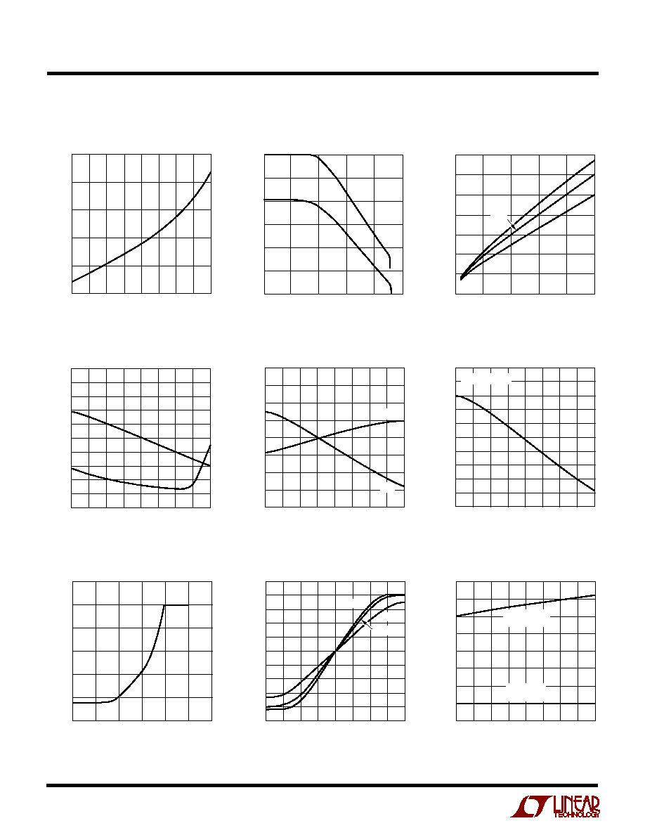
TYPICAL PERFOR
M
A
N
CE CHARACTERISTICS
U
W
SWITCH CURRENT (A)
0
0.7
0.6
0.5
0.4
0.3
0.2
0.1
0
0.6
1533 G03
0.2
0.4
0.8
125
°
C
25
°
C
1.0
SWITCH VOLTAGE (V)
85
°
C
DUTY CYCLE (%)
0
I
LIM
(mA)
0
50
100
150
200
250
300
10
20
30
125
°
C
25
°
C
40
1533 G02
50
Change in I
LIM
vs DC
Switch Voltage Drop
TEMPERATURE (
°
C)
50
NEGATIVE FEEDBACK VOLTAGE (V)
NFB INPUT CURRENT (
µ
A)
150
1533 G05
0
50
100
2.30
2.35
2.40
2.45
2.50
2.55
2.60
2.65
2.70
35
30
25
20
15
25
25
75
125
V
NFB
I
NFB
Negative Feedback Voltage and
Input Current vs Temperature
Feedback Voltage and Input
Current vs Temperature
Switching Frequency vs
Feedback Pin Voltage
FEEDBACK PIN VOLTAGE (V)
0
SWITCHING FREQUENCY (% TYPICAL)
0.1
0.2
0.3
0.4
1533 G07
0.5
120
100
80
60
40
20
0
0.6
Error Amplifier Output Current
FEEDBACK PIN VOLTAGE FROM NOMINAL (mV)
400 300 200 100
ERROR AMPLIFIER OUTPUT (
µ
A)
400
1533 G08
0
100
300
200
500
400
300
200
100
0
100
200
300
400
500
125
°
C
40
°
C
25
°
C
TEMPERATURE (
°
C)
V
C
PIN VOLTAGE (V)
1533 G09
1.6
1.4
1.2
1.0
0.8
0.6
0.4
0.2
0
50
25
75
25
0
50
100 125
V
C
PIN CLAMP
VOLTAGE
V
C
PIN
THRESHOLD
V
C
Pin Threshold and Clamp
Voltage vs Temperature
TEMPERATURE (
°
C)
50
FEEDBACK VOLTAGE (V)
FEEDBACK INPUT CURRENT (
µ
A)
1.30
1.29
1.28
1.27
1.26
1.25
1.24
1.23
1.22
1.21
1.20
2.0
1.8
1.6
1.4
1.2
1.0
0.8
0.6
0.4
0.2
0
0
50
75
1533 G04
25
25
V
FB
I
FB
100 125
150
JUNCTION TEMPERATURE (
°
C)
INPUT VOLTAGE (V)
2.60
2.65
2.70
1533 G01
2.55
2.50
2.45
50
0
50
75
25
25
100 125
150
Minimum Input Voltage vs
Temperature
TEMPERATURE (
°
C)
TRANSCONDUCTANCE (mho)
1533 G06
2000
1900
1800
1700
1600
1500
1400
1300
1200
1100
1000
50
25
75
150
25
0
50
100 125
g
m
=
I
VC
/
V
FB
Error Amplifier Transconductance
vs Temperature

5
LT1533
PI
N
FU
N
CTIO
N
S
U
U
U
GND (Pin 9): Signal Ground. The internal error amplifier,
negative feedback amplifier, oscillator, slew control cir-
cuitry and the bandgap reference are referred to this
ground. Keep the connection to the feedback divider and
V
C
compensation network free of large ground currents.
V
C
(Pin 10): The compensation pin is used for frequency
compensation and current limiting. It is the output of the
error amplifier and the input of the current comparator.
Loop frequency compensation can be performed with an
RC network connected from the V
C
pin to ground.
SHDN (Pin 11): The shutdown pin is used for disabling the
switcher. Grounding this pin will disable all internal cir-
cuitry. Normally this output can be tied high (to V
IN
) or may
be left floating.
R
CSL
(Pin 12): A resistor to ground sets the current slew
rate for the collectors A and B. The minimum resistor value
is 3.9k and the maximum value is 68k. Current slew will be
approximately:
I
SLEW(A/
µ
s)
= 33/R
CSL(k
)
R
VSL
(Pin 13): A resistor to ground sets the voltage slew
rate for the collectors A and B. The minimum resistor value
is 3.9k and the maximum value is 68k. Voltage slew will be
approximately:
V
SLEW(V/
µ
s)
= 220/R
VSL(k
)
V
IN
(Pin 14): Input Supply Pin. Bypass this pin with a
4.7
µ
F low ESR capacitor. When V
IN
is below 2.55V the
part will go into undervoltage lockout where it will stop
output switching and pull the V
C
pin low.
PGND (Pin 16): Power Switch Ground. This ground comes
from the emitters of the power switches. In normal opera-
tion this pin should have approximately 25nH inductance
to ground. This can be done by trace inductance (approxi-
mately 1") or with wire or a specific inductive component.
This inductance ensures stability in the current slew
control loop during turn-off. Too much inductance (>50nH)
may produce oscillation on the output voltage slew edges.
COL A, COL B (Pins 2, 15): These are the output collectors
of the power switches. Their emitters return to PGND
through a common sense resistor. COL A and
COL B are alternately turned on out of phase. Large
currents flow into these pins so it is desirable to keep
external trace lengths short to minimize radiation. The
collectors can be tied together for simple boost applica-
tions.
DUTY (Pin 3): Tying the DUTY pin to ground will force the
outputs to switch with a 50% duty cycle. The DUTY pin
must float if not used.
SYNC (Pin 4): The SYNC pin can be used to synchronize
the oscillator to an external clock (see Oscillator Sync in
Applications Information section for more details). The
SYNC pin may either be floated or tied to ground if not
used.
C
T
(Pin 5): The oscillator capacitor pin is used in conjunc-
tion with R
T
to set the oscillator frequency. For R
T
= 16.9k,
C
T(NF)
= 129/f
OSC(kHz)
R
T
(Pin 6): The oscillator resistor pin is used to set the
charge and discharge currents of the oscillator capacitor.
The nominal value is 16.9k. It is possible to adjust this
resistance
±
25% to get a more accurate oscillator fre-
quency.
FB (Pin 7): The feedback pin is used for positive voltage
sensing and oscillator frequency shifting during start-up
and short-circuit conditions. It is the inverting input to the
error amplifier. The noninverting input of this amplifier
connects internally to a 1.25V reference. This pin should
be left open if not used.
NFB (Pin 8): The negative voltage feedback pin is used for
sensing a negative output voltage. The pin is connected to
the inverting input of the negative feedback amplifier
through a 100k source resistor. The negative feedback
amplifier provides a gain of 0.5 to the feedback amplifier.
The nominal regulation point would be 2.5V on NFB. This
pin should be left open if not used.