 | ÐлекÑÑоннÑй компоненÑ: LT1537C | СкаÑаÑÑ:  PDF PDF  ZIP ZIP |
Äîêóìåíòàöèÿ è îïèñàíèÿ www.docs.chipfind.ru
1
LT1537
Advanced Low Power
5V RS232 Transceiver with
Small Capacitors
D
U
ESCRIPTIO
S
FEATURE
The LT
®
1537 is a three-driver, five-receiver RS232 trans-
ceiver, pin compatible with the LT1137A, offering perfor-
mance improvements and two shutdown modes. The
LT1537's charge pump is designed for extended compli-
ance and can deliver over 35mA of load current. Supply
current is typically 8mA, competitive with similar CMOS
devices. An advanced driver output stage operates up to
250kbaud while driving heavy capacitive loads.
The LT1537 is fully compliant with all RS232 specifica-
tions. Special bipolar construction techniques protect the
drivers and receivers beyond the fault conditions stipu-
lated for RS232. Driver outputs and receiver inputs can be
shorted to
±
25V without damaging the device or the
power supply generator. In addition, the RS232 I/O pins
are resilient to multiple
±
5kV ESD strikes.
The transceiver has two shutdown modes. One mode
disables the drivers and the charge pump, the other shuts
down all circuitry. While shut down, the drivers and
receivers assume high impedance output states.
, LTC and LT are registered trademarks of Linear Technology Corporation.
s
Low Cost
s
Uses Small Capacitors: 0.1
µ
F, 0.2
µ
F
s
1
µ
A Supply Current in Shutdown
s
120kBaud Operation for R
L
= 3k, C
L
= 2500pF
s
250kBaud Operation for R
L
= 3k, C
L
= 1000pF
s
CMOS Comparable Low Power: 40mW
s
Operates from a Single 5V Supply
s
Easy PC Layout: Flow-through Architecture
s
Rugged Bipolar Design
s
Outputs Assume a High Impedance State When Off
or Powered Down
s
Improved Protection: RS232 I/O Lines Can Be Forced
to
±
25V Without Damage
s
Output Overvoltage Does Not Force Current Back
into Supplies
s
Absolutely No Latch-Up
s
Available in SO Package
U
S
A
O
PPLICATI
s
Notebook Computers
s
Palmtop Computers
U
A
O
PPLICATI
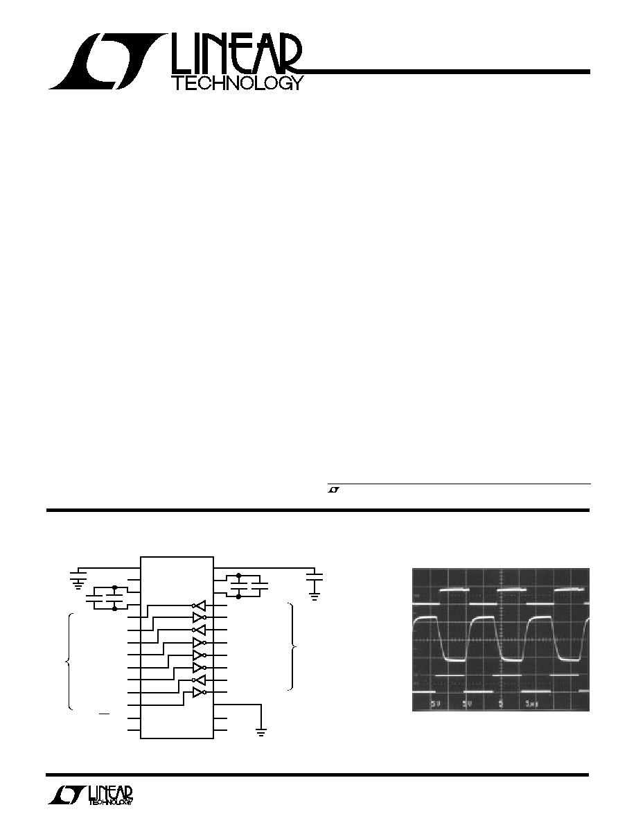
TYPICAL
R
LT1537 · TA02
LT1537 · TA01
5V V
CC
0.1
µ
F
2
×
0.1
µ
F
0.1
µ
F
TO
LINE
LT1537
1
2
3
4
5
6
7
8
9
10
11
12
13
14
DRIVER OUT
RX IN
DRIVER OUT
RX IN
RX IN
RX IN
DRIVER OUT
RX IN
28
27
26
25
24
23
22
21
20
19
18
17
16
15
2
×
0.1
µ
F
DRIVER IN
RX OUT
DRIVER IN
RX OUT
RX OUT
RX OUT
DRIVER IN
RX OUT
+
+
+
TO LOGIC
V
V
+
ON/OFF = 5V
+
DRIVER
DISABLE
GND
INPUT
DRIVER
OUTPUT
R
L
= 3k
C
L
= 2500pF
RECEIVER
OUTPUT
C
L
= 50pF
Output Waveforms
2
LT1537
(Note 1)
A
U
G
W
A
W
U
W
A
R
BSOLUTE
XI
TI
S
W
U
U
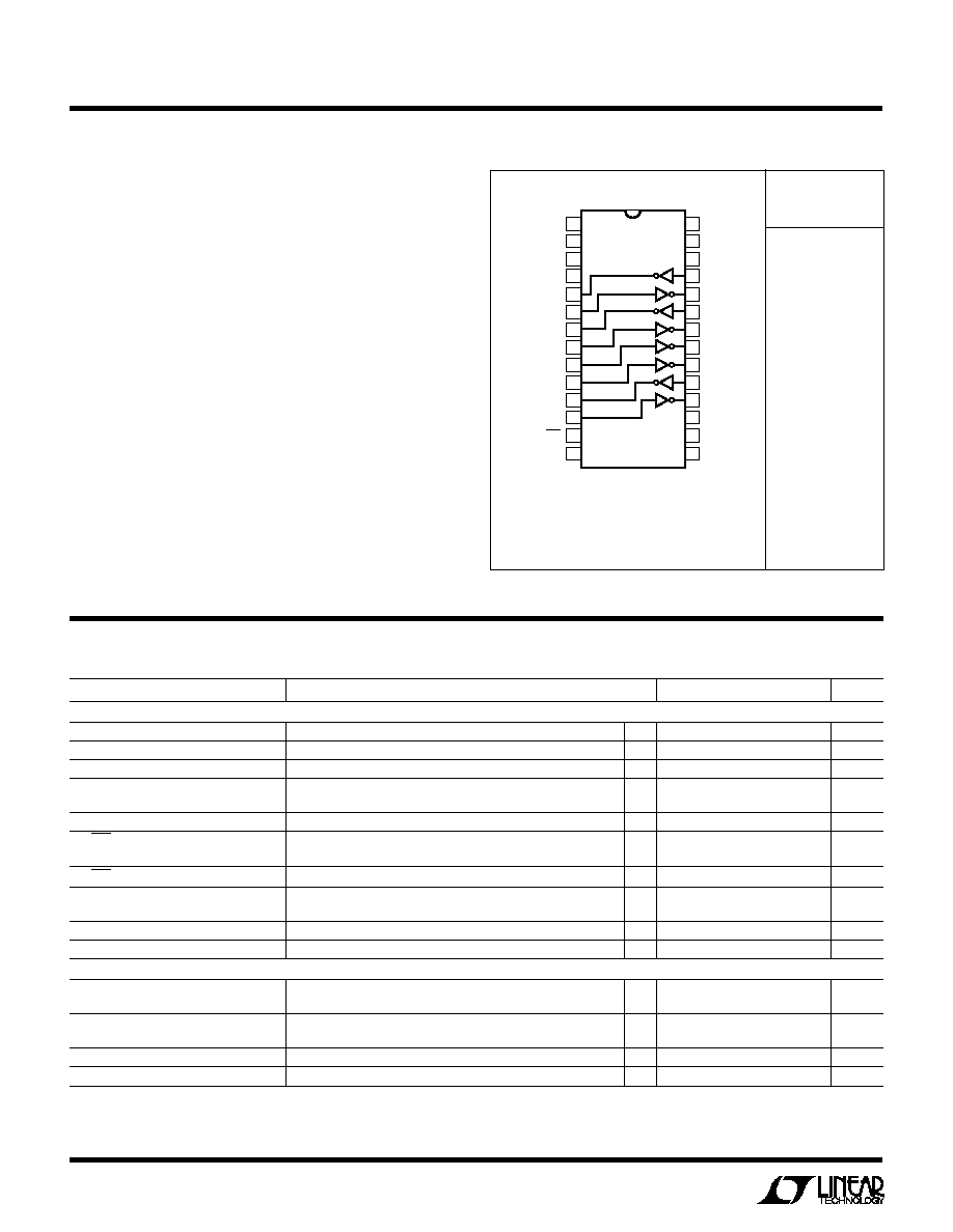
PACKAGE/ORDER I FOR ATIO
ORDER PART
NUMBER
Supply Voltage (V
CC
) ............................................. 5.5V
V
+
........................................................................ 13.2V
V
(Note 7) .......................................................... 6.5V
Input Voltage
Driver ........................................................... V
to V
+
Receiver ............................................... 25V to 25V
Output Voltage
Driver ....................................... V
+
25V to V
+
25V
Receiver .................................... 0.3V to V
CC
+ 0.3V
Short Circuit Duration
V
+
................................................................... 30 sec
V
................................................................... 30 sec
Driver Output .............................................. Indefinite
Receiver Output .......................................... Indefinite
Operating Temperature Range
LT1537C ................................................. 0
°
C to 70
°
C
Storage Temperature Range ................ 65
°
C to 150
°
C
Lead Temperature (Soldering, 10 sec)................. 300
°
C
Consult factory for Industrial and Military grade parts.
LT1537CG
LT1537CSW
ELECTRICAL C
C
HARA TERISTICS
(Note 2)
PARAMETER
CONDITIONS
MIN
TYP
MAX
UNITS
Power Supply Generator
V
+
Output
8.6
V
V
Output
7.0
V
Supply Current (V
CC
)
(Note 3)
q
8
17
mA
Supply Current When OFF (V
CC
)
Shutdown (Note 4)
q
1.0
10
µ
A
DRIVER DISABLE
1.5
mA
Shutdown to Turn-On
C
+
, C
= 0.1
µ
F, C1, C2 = 0.2
µ
F
0.2
ms
ON/OFF Pin Thresholds
Input LOW Level (Device Shutdown)
q
1.4
0.8
V
Input HIGH Level (Device Enabled)
q
2.4
1.4
V
ON/OFF Pin Current
0V
V
ON/OFF
5V
q
15
80
µ
A
Driver Disable Pin Thresholds
Input LOW Level (Drivers Enabled)
q
1.4
0.8
V
Input HIGH Level (Drivers Disabled)
q
2.4
1.4
V
Driver Disable Pin Current
0V
V
DRIVER DISABLE
5V
q
10
500
µ
A
Oscillator Frequency
130
kHz
Any Driver
Output Voltage Swing
Load = 3k to GND
Positive
q
5.0
7.5
V
Negative
q
6.3
5.0
V
Logic Input Voltage Level
Input LOW Level (V
OUT
= HIGH)
q
1.4
0.8
V
Input HIGH Level (V
OUT
= LOW)
q
2
1.4
Logic Input Current
0.8V
V
IN
2V
q
5
20
µ
A
Output Short-Circuit Current
V
OUT
= 0V
±
17
mA
1
2
3
4
5
6
7
8
9
10
11
12
13
14
V
+
5V V
CC
C1
+
C1
DRIVER OUT
RX IN
DRIVER OUT
RX IN
RX IN
RX IN
DRIVER OUT
RX IN
ON/OFF
NC
28
27
26
25
24
23
22
21
20
19
18
17
16
15
V
C2
C2
+
DRIVER IN
RX OUT
DRIVER IN
RX OUT
RX OUT
RX OUT
DRIVER IN
RX OUT
GND
NC
TOP VIEW
SW PACKAGE
28-LEAD PLASTIC SO WIDE
G PACKAGE
28-LEAD PLASTIC SSOP
DRIVER
DISABLE
T
JMAX
= 150
°
C,
JA
= 96
°
C/ W (G)
T
JMAX
= 150
°
C,
JA
= 85
°
C/ W (SW)
3
LT1537
ELECTRICAL C
C
HARA TERISTICS
PARAMETER
CONDITIONS
MIN
TYP
MAX
UNITS
Any Driver
Output Leakage Current
Shutdown V
OUT
=
±
15V (Note 4)
q
10
100
µ
A
Data Rate
R
L
= 3k, C
L
= 2500pF
120
kBaud
R
L
= 3k, C
L
= 1000pF
250
kBaud
Slew Rate
R
L
= 3k, C
L
= 51pF
15
30
V/
µ
s
R
L
= 3k, C
L
= 2500pF
4
15
V/
µ
s
Propagation Delay
Output Transition t
HL
HIGH to LOW (Note 5)
0.6
1.3
µ
s
Output Transition t
LH
LOW to HIGH
0.5
1.3
µ
s
Any Receiver
Input Voltage Thresholds
Input LOW Threshold (V
OUT
= HIGH)
q
0.8
1.3
V
Input HIGH Threshold (V
OUT
= LOW)
q
1.7
2.4
V
Hysteresis
q
0.1
0.4
1.0
V
Input Resistance
V
IN
=
±
10V
3
5
7
k
Output Voltage
Output LOW, I
OUT
= 1.6mA
q
0.2
0.4
V
Output HIGH, I
OUT
= 160
µ
A (V
CC
= 5V)
q
3.5
4.2
V
Output Leakage Current
Shutdown (Note 4) 0
V
OUT
V
CC
q
1
10
µ
A
Output Short-Circuit Current
Sinking Current, V
OUT
= V
CC
20
10
mA
Sourcing Current, V
OUT
= 0V
10
20
mA
Propagation Delay
Output Transition t
HL
HIGH to LOW (Note 6)
250
600
ns
Output Transition t
LH
LOW to HIGH
350
600
ns
The
q
denotes specifications which apply over the operating temperature
range (0
°
C
T
A
70
°
C for commercial grade and 40
°
C
T
A
85
°
C for
industrial grade).
Note 1: Absolute Maximum Ratings are those values beyond which the life
of the device may be impaired.
Note 2: Testing done at V
CC
= 5V and V
ON/OFF
= 3V. C1 = C2 = 0.2
µ
F,
C
+
= C
= 0.1
µ
F.
Note 3: Supply current is measured with driver and receiver outputs
unloaded and the driver inputs tied high.
Note 4: Supply current and leakage current measurements in shutdown
are performed with V
ON/OFF
= 0.1V. Supply current measurements using
DRIVER DISABLE are performed with V
DRIVER DISABLE
= 3V.
Note 5: For driver delay measurements, R
L
= 3k and C
L
= 51pF. Trigger
points are set between the driver's input logic threshold and the output
transition to the zero crossing (t
HL
= 1.4V to 0V and t
LH
= 1.4V to 0V).
Note 6: For receiver delay measurements, C
L
= 51pF. Trigger points are set
between the receiver's input logic threshold and the output transition to
standard TTL/CMOS logic threshold (t
HL
= 1.3V to 2.4V and t
LH
= 1.7V to
0.8V).
Note 7: Absolute maximum externally applied voltage. Internal charge
pump may force a larger value on this pin.
C
C
HARA TERISTICS
U
W
A
TYPICAL PERFOR
CE
(Note 2)
Driver Output Voltage
Receiver Input Thresholds
Supply Current vs Data Rate
DATA RATE (kBAUD)
0
SUPPLY CURRENT (mA)
30
40
50
75
125
LTX1537 · TPC03
20
10
0
25
50
100
60
70
80
150
3 DRIVERS ACTIVE
R
L
= 3k
C
L
= 2500pF
TEMPERATURE (
°
C)
55
0.50
THRESHOLD VOLTAGE (V)
0.75
1.25
1.50
1.75
3.00
2.25
0
50
75
ILT1537 · TPC02
1.00
2.50
2.75
2.00
25
25
100
125
INPUT HIGH
INPUT LOW
TEMPERATURE (
°
C)
50
10
DRIVER OUTPUT VOLTAGE (V)
8
4
2
0
10
4
0
50
75
LT1537 · TPC01
6
6
8
2
25
25
100
125
V
CC
= 5V
V
CC
= 5.5V
V
CC
= 4.5V
V
CC
= 5.5V
V
CC
= 4.5V
V
CC
= 5V
OUTPUT LOW
OUTPUT HIGH
R
L
= 3k
4
LT1537
C
C
HARA TERISTICS
U
W
A
TYPICAL PERFOR
CE
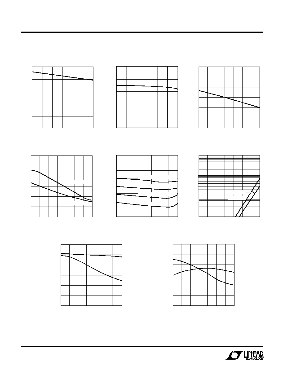
Driver Disable Threshold
Positive Supply Output
Compliance Curve
Negative Supply Output
Compliance Curve
NEGATIVE LOAD CURRENT (mA)
0
0
NEGATIVE SUPPLY OUTPUT (V)
2
4
6
8
10
5
10
LT1537 · TPC05
15
POSITIVE LOAD CURRENT (mA)
0
0
POSITIVE SUPPLY OUTPUT (V)
2
4
6
8
10
5
10
LT1537 · TPC04
15
TEMPERATURE (
°
C)
55
0
THRESHOLD VOLTAGE (V)
1.0
0.5
2.0
3.0
1.5
2.5
25
0
25
50
LT1537 · TPC06
75
100
125
On/Off Thresholds
Driver Leakage in Shutdown
Supply Current
TEMPERATURE (
°
C)
55
0
THRESHOLD VOLTAGE (V)
1.0
0.5
2.0
3.0
1.5
2.5
25
0
25
50
LT1537 · TPC07
75
100
125
ON THRESHOLD
OFF THRESHOLD
TEMPERATURE (
°
C)
0.1
LEAKAGE CURRENT (
µ
A)
10
100
LT1537 · TPC09
1
55
0
50
75
25
25
100
125
V
OUT
= 15V
V
OUT
= 15V
TEMPERATURE (
°
C)
55
SUPPLY VOLTAGE (mA)
35
25
LT1537 · TPC08
20
10
25
0
50
5
0
40
30
25
15
75
100
125
3 DRIVERS LOADED R
L
= 3k
2 DRIVERS LOADED R
L
= 3k
1 DRIVERS LOADED R
L
= 3k
NO LOAD
20kBAUD
Receiver Short-Circuit Current
Driver Output Short-Circuit Current
TEMPERATURE (
°
C)
55
SHORT-CIRCUIT CURRENT (mA)
20
25
30
25
75
LT1537 · TPC10
15
10
25
0
50
100
125
5
0
I
SC
+
I
SC
TEMPERATURE (
°
C)
55
SHORT-CIRCUIT CURRENT (mA)
20
25
30
25
75
LT1537 · TPC11
15
10
25
0
50
100
125
5
0
I
SC
+
I
SC
5
LT1537
C
C
HARA TERISTICS
U
W
A
TYPICAL PERFOR
CE
Shutdown to Driver Output
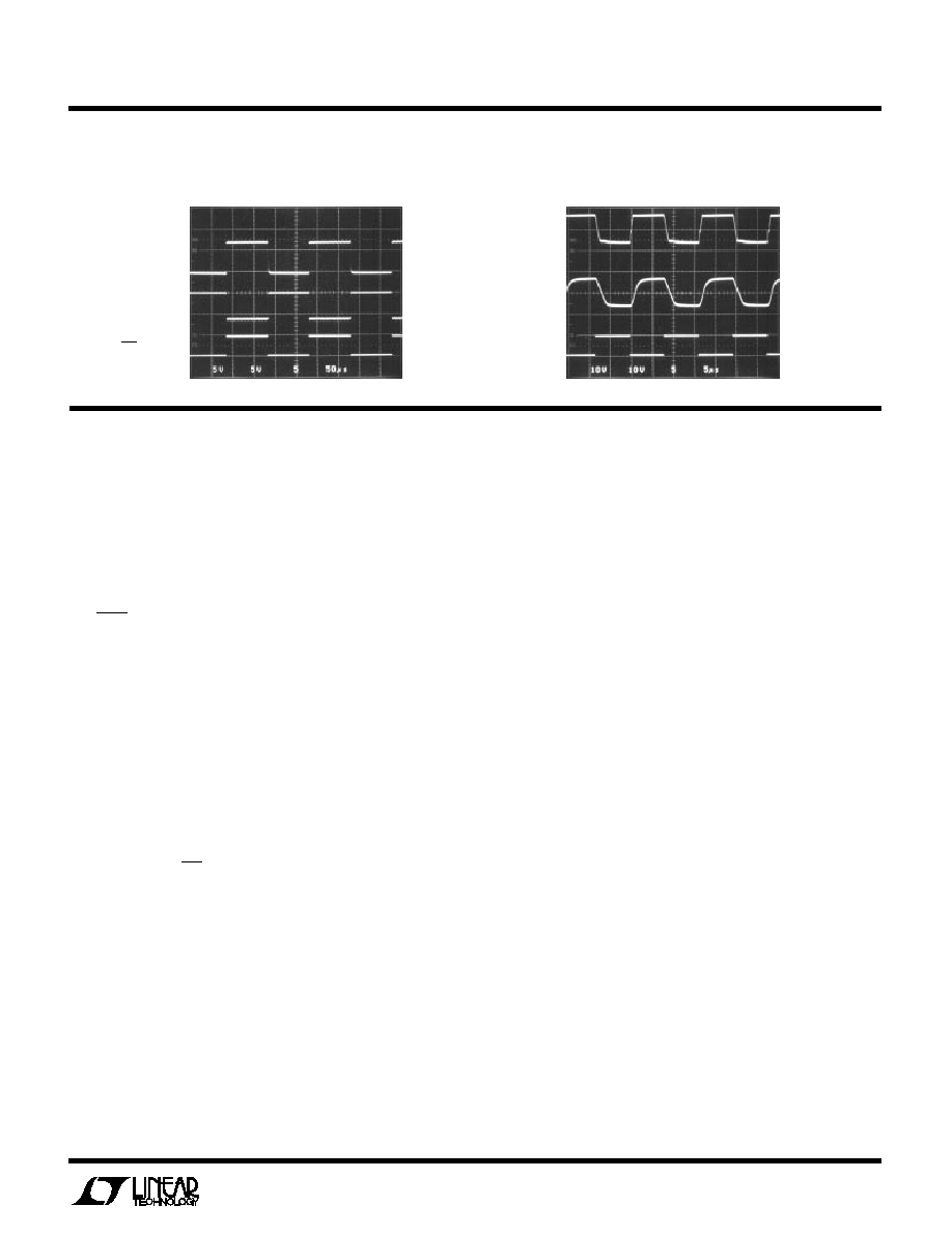
Driver Output Waveforms
LT1537 · TPC12
10
5
0
10
5
DRIVER OUTPUT
R
L
= 3k
C
L
= 2500pF
INPUT
DRIVER OUTPUT
R
L
= 3k
LT1537 · TPC13
DRIVER
OUTPUT HIGH
R
L
= 3k
ON/OFF PIN
DRIVER
OUTPUT LOW
R
L
= 3k
PI FU CTIO S
U
U
U
V
CC
: 5V Input Supply Pin. Supply current drops to zero in
the shutdown mode. This pin should be decoupled with a
0.1
µ
F ceramic capacitor close to the package pin. Insuffi-
cient supply bypassing can result in low output drive levels
and erratic charge pump operation.
GND: Ground Pin.
ON/OFF: TTL/CMOS Compatible Operating Mode Control.
A logic LOW puts the device in the shutdown mode which
reduces input supply current to zero and places all of the
drivers and receivers in high impedance state. A logic
HIGH fully enables the transceiver.
DRIVER DISABLE: This pin provides an alternate control
for the charge pump and RS232 drivers. A logic HIGH on
this pin shuts down the charge pump and places all drivers
in a high impedance state. Receivers remain active under
these conditions. Floating the driver disable pin or driving
it to a logic LOW level fully enables the transceiver. A logic
LOW on the On/Off pin supersedes the state of the Driver
Disable pin. Supply current drops to 1.5mA when in
DRIVER DISABLE mode.
V
+
: Positive Supply Output (RS232 Drivers). V
+
2V
CC
1.5V. This pin requires an external charge storage capaci-
tor C
0.1
µ
F, tied to ground or V
CC
. Larger value capaci-
tors may be used to reduce supply ripple. With multiple
transceivers, the V
+
and V
pins may be paralleled into
common capacitors. For large numbers of transceivers,
increasing the size of the shared common storage capaci-
tors is recommended to reduce ripple.
V
: Negative Supply Output (RS232 Drivers). V
(2V
CC
2.5V). This pin requires an external charge
storage capacitor C
0.1
µ
F. V
is short-circuit proof for
30 seconds.
C1
+
, C1
, C2
+
, C2
: Commutating Capacitor Inputs. These
pins require two external capacitors C
0.2
µ
F: one from
C1
+
to C1
and another from C2
+
to C2
. To maintain
charge pump efficiency, the capacitor's effective series
resistance should be less than 2
. Low ESR ceramic
capacitors work well in this application.
DRIVER IN: RS232 Driver Input Pins. These inputs are
TTL/CMOS compatible. Inputs should not be allowed to
float. Tie unused inputs to V
CC
.
DRIVER OUT: Driver Outputs at RS232 Voltage Levels.
Driver output swing meets RS232 levels for loads up to 3k.
Slew rates are controlled for lightly loaded lines. Output
current capability is sufficient for load conditions up to
2500pF. Outputs are in a high impedance state when in
shutdown mode, V
CC
= 0V or when the driver disable pin
is active. Outputs are fully short-circuit protected from V
+ 25V to V
+
25V. Applying higher voltages will not
damage the device if the overdrive is moderately current
limited. Short circuits on one output can load the power
supply generator and may disrupt the signal levels of the
other outputs. The driver outputs are protected against
ESD to
±
5kV for human body model discharges.