1567f.pm6
LT1567
1
1567f
The LT
®
1567 is an analog building block optimized for
very low noise high frequency filter applications. It con-
tains two wideband rail-to-rail operational amplifiers, one
of them internally configured as a unity-gain inverter.
With the addition of a few passive components, the
LT1567 becomes a flexible second order filter section
with cutoff frequency (f
C
) up to 5MHz, ideal for antialias-
ing or for channel filtering in high speed data communi-
cations systems. A spreadsheet-based design tool is
available at www.linear.com for designing lowpass and
bandpass filters using the LT1567.
In addition to low noise and high speed, the LT1567
features single-ended to differential conversion for direct
driving of high speed differential input A/D converters. The
LT1567 operates from a total power supply voltage of 2.7V
to 12V and supports signal-to-noise ratios above 100dB.
The LT1567 is available in an 8-lead MSOP package.
, LTC and LT are registered trademarks of Linear Technology Corporation.
s
Low Noise, High Speed Filters to 5MHz
s
Low Noise Differential Circuits
s
Communication Channel or Roofing Filters
s
Antialias or Reconstruction Filtering
s
Video Signal Processing
s
Single-Ended to Differential Conversion
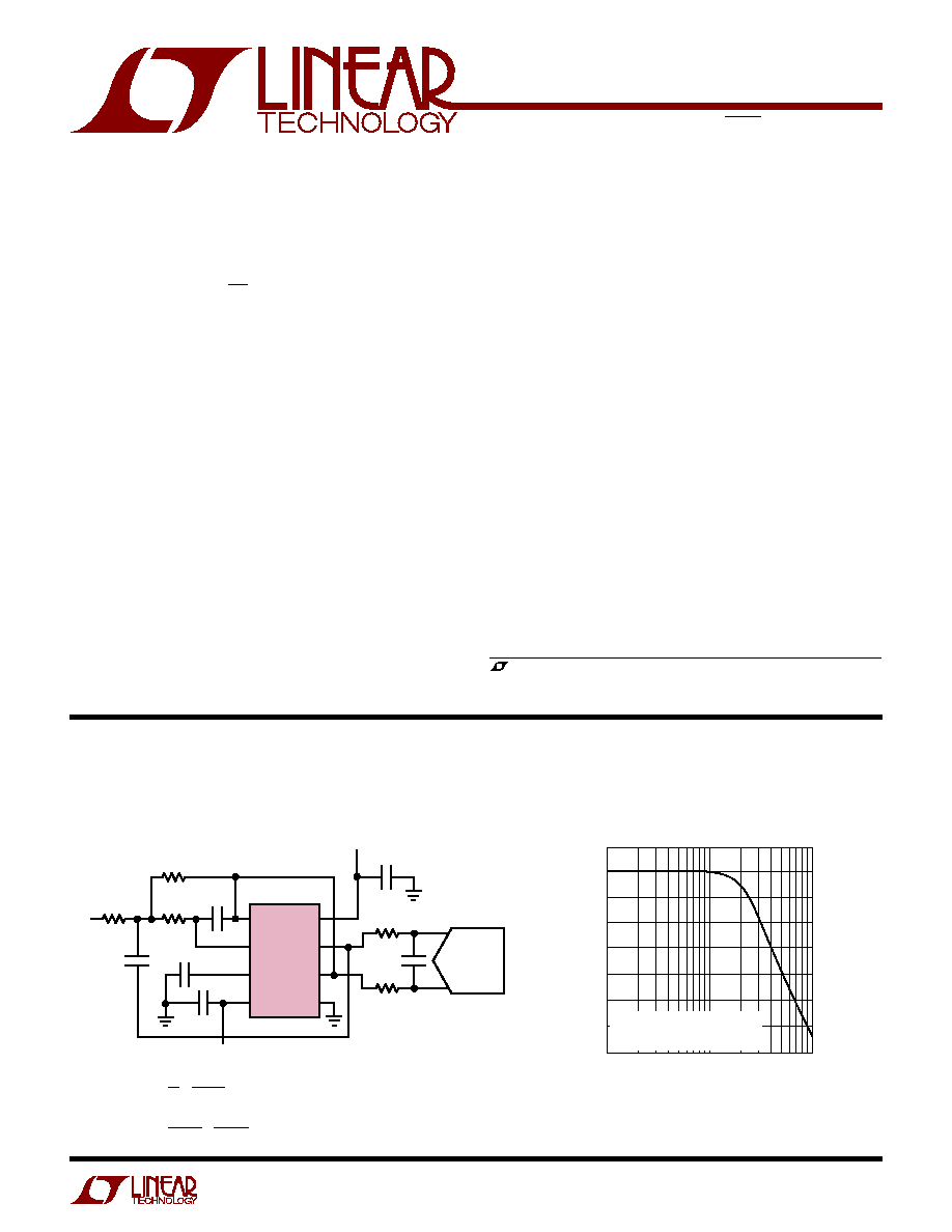
2MHz 3-Pole Antialias Filter with
Single-Ended to Differential Conversion
Frequency Response
s
Single-Ended to Differential Conversion
s
Low Noise: 1.4nV/
Hz
s
20
µ
V
RMS
Total Wideband Noise in Filter
with 2MHz f
C
s
Dynamic Range: 104dB SNR at
±
5V
s
Total Supply Voltage: 2.7V to 12V
s
Rail-to-Rail Outputs
s
DC Accurate: Op Amp V
OS
0.5mV (Typ)
s
Trimmed Bandwidth for Accurate Filters
s
MSOP-8 Surface Mount Package
s
No External Clock Required
1.4nV/
Hz 180MHz
Filter Building Block
FREQUENCY (Hz)
100
GAIN (dB)
12
6
0
6
12
18
24
30
36
1M
10M
1567 TA01a
NOTE: 6dB GAIN RESULTS FROM
SINGLE-ENDED TO DIFFERENTIAL
CONVERSION
DESCRIPTIO
U
FEATURES
APPLICATIO S
U
TYPICAL APPLICATIO
U
A
IN
+A
IN
ADC
1567 TA01
V
IN
0.1
µ
F
0.1
µ
F
C1
270pF
C3
270pF
C2
270pF
0.1
µ
F
V
V
+
1
2
3
4
8
7
6
5
R2
536
R3
147
R1
536
R4
147
R5
147
LTC1420
96dB DIFFERENTIAL SNR WITH 3V TOTAL SUPPLY
LT1567
R2
R1
GAIN =
2.5MHz
f
3dB
R3 = R4 = R5, C1 = C2 = C3
1.82
2
R2C2
f
3dB
=
=
f
3dB
2.5MHz
;
1
4
R3C3
LT1567
2
1567f
Total Supply Voltage (V
+
to V
) ............................ 12.6V
Input Current (Note 2) ........................................
±
25mA
Operating Temperature Range (Note 3)
LT1567C ..............................................40
°
C to 85
°
C
LT1567I ...............................................40
°
C to 85
°
C
Specified Temperature Range (Note 4)
LT1567C ..............................................40
°
C to 85
°
C
LT1567I ...............................................40
°
C to 85
°
C
Storage Temperature Range ................. 65
°
C to 150
°
C
Lead Temperature (Soldering, 10 sec).................. 300
°
C
ORDER PART
NUMBER
MS8 PART MARKING
T
JMAX
= 150
°
C,
JA
= 200
°
C/W
LTWH
LTWJ
LT1567CMS8
LT1567IMS8
(Note 1)
The
q
denotes the specifications that apply over the full operating temperature range (Note 4), otherwise specifications and typical
values are at T
A
= 25
°
C. V
S
=
±
2.5V, R
L
= 1K, V
OUT
= 0 on both amplifiers unless otherwise noted.
PARAMETER
CONDITIONS
MIN
TYP
MAX
UNITS
Total Supply Voltage
2.7
12
V
Supply Current
V
S
=
±
1.5V
q
8.5
15
mA
V
S
=
±
2.5V
q
9
16
mA
V
S
=
±
5V
q
11
19
mA
OA Output Positive Voltage Swing
V
S
=
±
1.5V, R
L
= 1k
q
1.30
1.45
V
V
S
=
±
2.5V, R
L
= 1k
q
2.20
2.45
V
V
S
=
±
2.5V, R
L
=100
q
2.00
2.25
V
V
S
=
±
5V, R
L
= 1k
q
4.70
4.90
V
OA Output Negative Voltage Swing
V
S
=
±
1.5V, R
L
= 1k
q
1.30
1.45
V
V
S
=
±
2.5V, R
L
= 1k
q
2.20
2.45
V
V
S
=
±
2.5V, R
L
=100
q
2.00
2.30
V
V
S
=
±
5V, R
L
= 1k
q
4.70
4.90
V
INV Output Positive Voltage Swing
V
S
=
±
1.5V, R
L
= 1k
q
1.30
1.40
V
V
S
=
±
2.5V, R
L
= 1k
q
2.20
2.50
V
V
S
=
±
2.5V, R
L
= 100 (LT1567I Only, Note 5)
q
1.90
2.00
V
V
S
=
±
5V, R
L
= 1k
q
4.60
4.80
V
INV Output Negative Voltage Swing
V
S
=
±
1.5V, R
L
= 1k
q
1.30
1.40
V
V
S
=
±
2.5V, R
L
= 1k
q
2.20
2.40
V
V
S
=
±
2.5V, R
L
= 100 (LT1567I Only, Note 5)
q
1.90
2.00
V
V
S
=
±
5V, R
L
= 1k
q
4.50
4.80
V
Common Mode Input Voltage Range (DC BIAS, Pin 5)
V
S
=
±
1.5V, CMRR
40dB (Note 6)
q
0.5
0.5
V
(See Pin Functions)
V
S
=
±
5V, CMRR
40dB (Note 6)
q
3.8
3.5
V
DC Common Mode Rejection Ratio (CMRR)
V
S
=
±
1.5V, DC BIAS = 0.25V to 0.25V
q
90
dB
V
S
=
±
5V, DC BIAS = 2.5V to 2.5V
q
65
90
dB
DC Power Supply Rejection Ratio (PSRR)
V
S
=
±
1.5V to
±
5V, DC BIAS = 0V
q
80
100
dB
OA Input Offset Voltage
q
0.5
3
mV
INV Output Offset Voltage
q
5
9
mV
Consult LTC Marketing for parts specified with wider operating temperature ranges.
1
2
3
4
OAOUT
OAIN
BYPASS
V
8
7
6
5
V
+
INVOUT
INVIN
DC BIAS
TOP VIEW
MS8 PACKAGE
8-LEAD PLASTIC MSOP
ABSOLUTE AXI U RATI GS
W
W
W
U
PACKAGE/ORDER I FOR ATIO
U
U
W
ELECTRICAL CHARACTERISTICS
LT1567
3
1567f
Note 1: Absolute Maximum Ratings are those values beyond which the life
of a device may be impaired.
Note 2: The inputs of each op amp are protected by back-to-back diodes
and diodes to each supply. If either input exceeds the supply or the
differential input voltage exceeds 1.4V, the input current should be limited
to less than 25mA.
Note 3: The LT1567C and LT1567I are guaranteed functional over the
operating temperature range 40
°
C to 85
°
C.
Note 4: The LT1567C is guaranteed to meet specified performance from
0
°
C to 70
°
C. The LT1567C is designed, characterized and expected to
meet specified performance from 40
°
C to 85
°
C but not tested or QA
sampled at these temperatures. The LT1567I is guaranteed to meet
specified performance from 40
°
C to 85
°
C.
PARAMETER
CONDITIONS
MIN
TYP
MAX
UNITS
OA Input Bias Current
q
3
10
µ
A
DC BIAS Input Bias Current
q
6
15
µ
A
OA DC Open-Loop Gain
V
S
=
±
1.5V, R
L
= 1k, V
O
= 1V to 1V
q
7.5
55
V/mV
V
S
=
±
2.5V, R
L
= 1k, V
O
= 2V to 2V
q
10
60
V/mV
V
S
=
±
2.5V, R
L
= 100, V
O
= 1.5V to 1.5V
q
1.2
7.0
V/mV
V
S
=
±
5V, R
L
= 1k, V
O
= 4V to 4V
q
15
80
V/mV
INV DC Gain
V
S
=
±
1.5V, R
L
= 1k, V
IN
= 1V to 1V
q
0.97
1.04
V/V
V
S
=
±
2.5V, R
L
= 1k, V
IN
= 2V to 2V
q
0.97
1.04
V/V
V
S
=
±
2.5V, R
L
= 100, V
IN
= 1.5V to 1.5V
q
0.97
1.04
V/V
V
S
=
±
5V, R
L
= 1k, V
IN
= 4V to 4V
q
0.97
1.04
V/V
INV DC Input Resistance
V
S
=
±
2.5V, R
L
= 1k, V
IN
= 2V to 2V
q
450
600
750
OA Gain Bandwidth Product
Measured at 2MHz, V
S
=
±
1.5V
q
100
180
MHz
Measured at 2MHz, V
S
=
±
2.5V
q
110
185
MHz
Measured at 2MHz, V
S
=
±
5V
q
120
190
MHz
INV Bandwidth
3dB
85
MHz
INV AC Gain
Measured at 2MHz
q
0.96
1.0
1.05
V/V
OA Slew Rate
V
S
=
±
5V
55
V/
µ
s
INV Slew Rate
V
S
=
±
5V
90
V/
µ
s
OA Input Voltage Noise Density (Note 7)
f = 100kHz
1.4
nV/
Hz
OA Input Current Noise Density
f = 100kHz
1.0
pA/
Hz
Wideband Output Noise for a Second Order Filter (Figure 1)
f
C
= 2MHz, BW = 4MHz (Note 8)
20
µ
V
RMS
f
C
= 5MHz, BW = 10MHz (Note 8)
30
µ
V
RMS
Total Harmonic Distortion (THD)
f = 1MHz, f
C
= 2MHz, V
OUT
= 1V
RMS
88
dB
for a Second Order Filter (Figure 1)
f = 2.5MHz, f
C
= 5MHz, V
OUT
= 1V
RMS
70
dB
Output Short-Circuit Current (Either Output)
q
20
50
mA
OA Output Impedance
f = 100kHz, OA Connected as
0.03
Unity-Gain Inverter
INV Output Impedance
f = 100kHz
0.7
Note 5: With INVIN pin driven to
±
2V.
Note 6: This parameter is not 100% tested.
Note 7: The input referred voltage noise density of the unity gain inverter
is 5.6nV/
Hz which includes the noise of the gain setting resistors.
Note 8: For f
C
= 2MHz, C1 = C2 = 180pF, R1 = R2 = 604
, R3 = 316
and
for f
C
= 5MHz, C1 = C2 = 180pF, R1 = R2 = 232
, R1 = 130
. BW is the
bandwidth of the noise measurement (Figure 1 circuit).
ELECTRICAL CHARACTERISTICS
The
q
denotes the specifications that apply over the full operating temperature range (Note 4), otherwise specifications and typical
values are at T
A
= 25
°
C. V
S
=
±
2.5V, R
L
= 1K, V
OUT
= 0 on both amplifiers unless otherwise noted.
LT1567
4
1567f
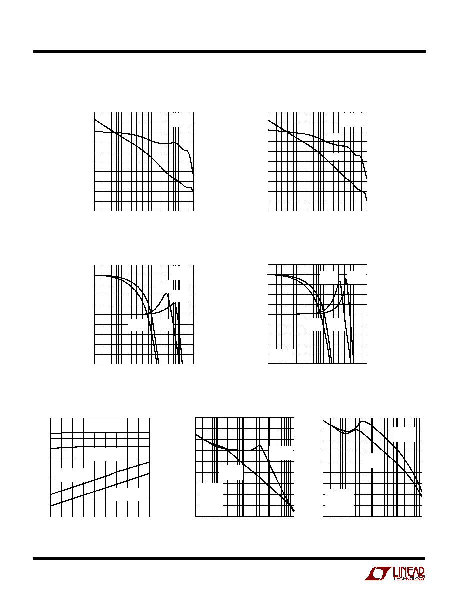
TYPICAL PERFOR A CE CHARACTERISTICS
U
W
OA Open-Loop Gain and Phase
vs Frequency
FREQUENCY (MHz)
0
GAIN (dB)
PHASE (DEG)
60
70
10
20
50
20
40
30
10
0.1
10
100
1567 G01
30
60
120
150
90
120
90
0
60
30
30
150
1
V
S
=
±
5V
T
A
= 25
°
C
PHASE
GAIN
FREQUENCY (MHz)
0
GAIN (dB)
PHASE (DEG)
60
70
10
20
50
20
40
30
10
0.1
10
100
1567 G02
30
60
120
150
90
120
90
0
60
30
30
150
1
V
S
=
±
1.5V
T
A
= 25
°
C
PHASE
GAIN
FREQUENCY (MHz)
4
GAIN (dB)
PHASE (DEG)
8
10
6
8
6
0
4
2
2
0.1
10
100
1567 G03
10
168
180
182
166
164
178
172
176
174
170
162
1
V
S
=
±
5V
T
A
= 25
°
C
GAIN
OA OUT
PHASE
OA OUT
PHASE
INV OUT
GAIN
INV OUT
OA Open-Loop Gain and Phase
vs Frequency
Closed-Loop Gain and Phase of OA
and INV vs Frequency (A
V
= 1)
PSRR of OA vs Frequency
FREQUENCY (MHz)
20
POWER SUPPLY REJECTION (dB)
40
50
70
90
0.001
0.1
1
10
1567 G04
0
0.01
60
30
10
80
V
S
=
±
5V
A
V
= 10
R
F
= 1k
R
G
= 100
R
L
= 1k
POSITIVE
SUPPLY
NEGATIVE
SUPPLY
FREQUENCY (MHz)
20
POWER SUPPLY REJECTION (dB)
40
50
70
90
0.001
0.1
1
10
1567 G05
0
0.01
60
30
10
80
POSITIVE
SUPPLY
V
S
=
±
5V
A
V
= 1
R
F
= R
G
= 1k
R
L
= 1k
NEGATIVE
SUPPLY
PSRR of OA or INV vs Frequency
TEMPERATURE (
°
C)
55
150
GAIN BANDWIDTH (MHz)
PHASE MARGIN (DEG)
175
225
250
275
15
25
45
125
1567 G14
200
35
15
25
45
65
5
35
5
65
85 105
PHASE MARGIN
V
S
=
±
5V
PHASE MARGIN
V
S
=
±
1.5V
GBW PRODUCT
V
S
=
±
5V
GBW PRODUCT
V
S
=
±
1.5V
OA Gain Bandwidth Product and
Phase Margin vs Temperature
Closed-Loop Gain and Phase of OA
and INV vs Frequency (A
V
= 1)
FREQUENCY (MHz)
4
GAIN (dB)
PHASE (DEG)
8
10
6
8
6
0
4
2
2
0.1
10
100
1567 G15
10
168
180
182
166
164
178
172
176
174
170
162
1
V
S
=
±
1.5V
T
A
= 25
°
C
GAIN
INV OUT
PHASE
OA OUT
PHASE
INV OUT
GAIN
OA OUT

LT1567
5
1567f
TYPICAL PERFOR A CE CHARACTERISTICS
U
W
Input Voltage Noise Density of OA
vs Frequency
Input Current Noise Density of OA
vs Frequency
FREQUENCY (kHz)
0.1
2.5
3.0
3.5
4.0
4.5
1
10
100
1567 G10
2.0
1.5
0.5
0
1.0
VOLTAGE NOISE DENSITY (nV/
Hz)
T
A
= 25
°
C
Input Bias Current of OA
vs Common Mode Voltage
Supply Current vs Supply Voltage
COMMON MODE VOLTAGE (V)
0
INPUT BIAS CURRENT (
µ
A)
3
4
5
3
5
1567 G12
2
1
0
1
2
4
6
7
8
V
S
= 5V
TOTAL SUPPLY VOLTAGE (V)
0
SUPPLY CURRENT (mA)
10
15
8
1567 G13
5
0
2
4
6
10
20
FREQUENCY (kHz)
0.1
2.5
3.0
3.5
4.0
4.5
1
10
100
1567 G11
2.0
1.5
0.5
0
1.0
CURRENT NOISE DENSITY (pA/
Hz)
T
A
= 25
°
C
OA Rising Slew Rate
vs Temperature
TEMPERATURE (
°
C)
55
20
SLEW RATE (V/
µ
s)
30
40
50
60
35 15
5
25
1567 G07
45
65
85 105 125
V
S
=
±
5V
V
S
=
±
2.5V
V
S
=
±
1.5V
A
V
= 1
R
F
= R
G
= 1k
R
L
= 1k
CAPACITIVE LOAD (pF)
10
0
OVERSHOOT (%)
5
10
15
20
30
100
1000
1567 G08
25
V
S
=
±
2.5V
A
V
= 1
R
S
= 10
R
L
=
R
S
= 20
R
L
=
R
L
= R
S
= 50
Output Overshoot vs Series
Resistor and Capacitive Load
CAPACITIVE LOAD (pF)
10
0
OVERSHOOT (%)
10
20
40
100
1000
1567 G09
30
5
15
35
25
V
S
=
±
1.5V
A
V
= 1
R
S
= 10
R
L
=
R
S
= 20
R
L
=
R
S
= R
L
= 50
Output Overshoot vs Series
Resistor and Capacitive Load
FREQUENCY (Hz)
100k
0.001
OUTPUT IMPEDANCE (
)
0.1
100
1M
10M
100M
1567 G06
0.01
1
10
V
S
=
±
5V
T
A
= 25
°
C
OA
A
V
= 10
INVERTER
OA
A
V
= 1
Output Impedance vs Frequency