 | –≠–ª–µ–∫—Ç—Ä–æ–Ω–Ω—ã–π –∫–æ–º–ø–æ–Ω–µ–Ω—Ç: LT1568IGN | –°–∫–∞—á–∞—Ç—å:  PDF PDF  ZIP ZIP |
LT1568
1
1568f
The LT
Æ
1568 is an easy-to-use, active-RC filter building
block with rail-to-rail inputs and outputs. The internal ca-
pacitors of the IC and the GBW product of the internal low
noise op amps are trimmed such that consistent and repeat-
able filter responses can be achieved. With a single resis-
tor value, the LT1568 provides a pair of matched 2-pole
Butterworth lowpass filters with unity gain suitable for I/Q
channels.
By using unequal-valued external resistors, the two 2-pole
sections can create different frequency responses or
gains. In addition, the two stages may be cascaded to
create a single 4-pole filter with a programmable re-
sponse. Capable of cutoff frequencies up to 10MHz, the
LT1568 is ideal for antialiasing or channel filtering in high
speed data communications systems. The LT1568 can
also be used as a bandpass filter.
The LT1568 features very low noise, supporting signal-to-
noise ratios of over 90dB. It also provides single-ended to
differential signal conversion for directly driving high
speed A/D converters. The LT1568 has a shutdown mode
that reduces supply current to approximately 0.5mA on a
5V supply.
The LT1568 is available in a narrow 16-lead SSOP
package.
, LTC and LT are registered trademarks of Linear Technology Corporation.
s
Up to 10MHz Center Frequency on a Single 3V
Supply
s
Easy to Use--A Single Resistor Value Sets Lowpass
Cutoff Frequency (200kHz
C
5MHz), Unequal
Resistor Values Extend Cutoff Frequency Up to
10MHz
s
Extremely Flexible--Different Resistor Values
Allow Lowpass Transfer Functions with or Without
Gain (Butterworth, Chebyshev or Custom)
s
SNR = 92dB (
C
= 2MHz, 2V
P-P
)
s
THD = ≠84dB (
C
= 2MHz, 1V
P-P
)
s
Internal Capacitors Trimmed to
±
0.75%
s
Single 4-Pole Lowpass Filter or Matched Pair of
2-Pole Lowpass Filters
s
Can be Connected as a Bandpass Filter
s
Single-Ended or Differential Output
s
Operates from Single 3V (2.7V Min) to
±
5V Supply
s
Rail-to-Rail Input and Output Voltages
Very Low Noise,
High Frequency Active RC,
Filter Building Block
s
Replaces Discrete RC Active Filters and LC Filter
Modules
s
Antialiasing/Reconstruction Filters
s
Dual or I-and-Q Channels (Two Matched 2nd Order
Filters in One Package)
s
Single-Ended to Differential Conversion
s
Video Signal Processing
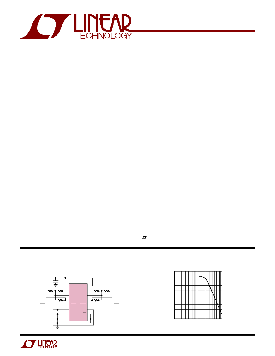
V
+
INVA
SA
OUTA
OUTA
GNDA
NC
V
≠
V
+
INVB
SB
OUTB
OUTB
GNDB
EN
V
≠
1
2
3
4
5
6
7
8
16
15
14
13
12
11
10
9
LT1568
511
0.1
µ
F
0.1
µ
F
511
511
511
511
1568 TA01
V
INA
3V
V
OUTA
V
OUTA
V
INB
THE PROPRIETARY ARCHITECTURE
ALLOWS FOR A SIMPLE RESISTOR
CALCULATION:
V
OUTB
V
OUTB
511
R = 128
∑
;
C
= CUTOFF FREQUENCY
10MHz
C
Amplitude and Phase Matched Dual Butterworth 2.5MHz Lowpass
Filter with Differential Output. Single 3V Supply Operation
FREQUENCY (Hz)
100k
≠27
GAIN (dB)
≠21
≠15
≠9
≠3
1M
10M
1568 TA02
3
≠24
≠18
≠12
≠6
0
Amplitude Response
DESCRIPTIO
U
FEATURES
APPLICATIO S
U
TYPICAL APPLICATIO
U
LT1568
2
1568f
Total Supply Voltage (V
+
to V
≠
) ........................... 11.6V
Input Voltage on INVA, INVB, GNDA and
GNDB Pins ....................................................... V
+
to V
≠
Input Current on INVA, INVB, GNDA and
GNDB Pins (Note 2) ...........................................
±
10mA
Output Short-Circuit Duration on OUTA, OUTB, OUTA
and OUTB Pins ............................................... Indefinite
Maximum Continuous Output Current (Note 3)
DC ...............................................................
±
100mA
Specified Temperature Range (Note 9)
LT1568C ............................................ ≠ 40
∞
C to 85
∞
C
LT1568I ............................................. ≠ 40
∞
C to 85
∞
C
Junction Temperature .......................................... 150
∞
C
Storage Temperature Range ................ ≠ 65
∞
C to 150
∞
C
Lead Temperature (Soldering, 10 sec)................. 300
∞
C
ORDER PART
NUMBER
(Note 1)
ABSOLUTE AXI U RATI GS
W
W
W
U
PACKAGE/ORDER I FOR ATIO
U
U
W
Consult LTC Marketing for parts specified with wider operating temperature ranges.
LT1568CGN
LT1568IGN
T
JMAX
= 150
∞
C,
JA
= 135
∞
C/W
The
q
denotes the specifications which apply over the full operating
temperature range, otherwise specifications and typical values are at T
A
= 25
∞
C. V
S
= single 5V, EN pin to logic "low," R
L
= 400
,
connected to midsupply, R
FIL
= R11 = R21 = R31 = R12 = R22 = R32, unless otherwise noted (see Block Diagram).
SYMBOL
PARAMETER
CONDITIONS
MIN
TYP
MAX
UNITS
V
S
Total Supply Voltage
q
2.7
11
V
I
S
Supply Current
V
S
= 3V
q
24
35
mA
V
S
= 5V
q
26
36
mA
V
S
=
±
5V
q
28
38
mA
Shutdown Supply Current
V
S
= 3V, V
EN
= 2.4V
q
0.3
1.0
mA
V
S
= 5V, V
EN
= 4.4V
q
0.5
1.3
mA
V
S
=
±
5V, V
EN
= 4.4V
q
1.0
2.5
mA
Output Voltage Swing High
V
S
= 3V, R
FIL
= 1.28k, R
L
= 1k
q
2.75
2.85
V
(OUTA, OUTA, OUTB, OUTB Pins)
V
S
= 5V, R
FIL
= 1.28k, R
L
= 1k
q
4.60
4.80
V
V
S
= 5V, R
FIL
= 128
, R
L
= 400
q
4.50
4.65
V
V
S
=
±
5V, R
FIL
= 1.28k, R
L
= 1k
q
4.60
4.75
V
Output Voltage Swing Low
V
S
= 3V, R
FIL
= 1.28k, R
L
= 1k
q
0.05
0.12
V
(OUTA, OUTA, OUTB, OUTB Pins)
V
S
= 5V, R
FIL
= 1.28k, R
L
= 1k
q
0.07
0.15
V
V
S
= 5V, R
FIL
= 128
, R
L
= 400
q
0.20
0.40
V
V
S
=
±
5V, R
FIL
= 1.28k, R
L
= 1k
q
≠4.7
V
I
OUT
Maximum Output Current
±
80
mA
Op Amp Input Offset Voltage
V
S
= 3V
q
≠2.5
≠0.5
1.5
mV
V
S
= 5V
q
≠2.5
0.2
2.5
mV
V
S
=
±
5V
q
≠2.0
1.2
4.5
mV
Inverter Output Offset Voltage
V
S
= 3V
q
≠2
2.5
7.0
mV
V
S
= 5V
q
≠10
0.6
4.5
mV
V
S
=
±
5V
q
≠12
≠4.0
2.0
mV
ELECTRICAL CHARACTERISTICS
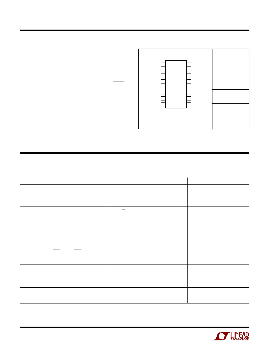
GN PACKAGE
16-LEAD PLASTIC SSOP
1
2
3
4
5
6
7
8
TOP VIEW
16
15
14
13
12
11
10
9
V
+
INVA
SA
OUTA
OUTA
GNDA
NC
V
≠
V
+
INVB
SB
OUTB
OUTB
GNDB
EN
V
≠
GN PART
MARKING
1568
1568I
LT1568
3
1568f
The
q
denotes the specifications which apply over the full operating
temperature range, otherwise specifications and typical values are at T
A
= 25
∞
C. V
S
= single 5V, EN pin to logic "low," R
L
= 400
,
connected to midsupply, R
FIL
= R11 = R21 = R31 = R12 = R22 = R32, unless otherwise noted (see Block Diagram).
SYMBOL
PARAMETER
CONDITIONS
MIN
TYP
MAX
UNITS
I
B
Op Amp Input Bias Current
V
S
= 3V
q
0.5
2
µ
A
V
S
= 5V
q
0.4
2
µ
A
V
S
=
±
5V
q
≠0.2
2
µ
A
Inverter Bandwidth (Note 4)
55
MHz
Inverter Gain (Sections A and B, Note 5)
Frequency = DC
q
≠0.2
0.01
0.2
dB
Frequency = 2MHz
0.01
dB
Frequency = 10MHz
0.27
dB
Inverter Phase Shift (Sections A and B,
Frequency = DC
180
DEG
Note 5)
Frequency = 2MHz
179
DEG
Frequency = 10MHz
176
DEG
SR
Slew Rate (OUTA, OUTB, OUTA,
53
V/
µ
s
OUTB) Pins
V
CM
Common Mode Input Voltage Range
V
S
= 3V
1 to 1.9
V
(GNDA and GNDB Pins, Note 6)
V
S
=
±
5V
≠3.4 to 2.7
V
Single Supply GND Reference Voltage
V
S
= 5V, GNDA Tied to GNDB
2.5
V
V
IL
EN Input Logic Low Level
V
S
= 3V, 5V or
±
5V
q
V
+
≠ 2.1
V
V
IH
EN Input Logic High Level
V
S
= 3V, 5V or
±
5V
q
V
+
≠ 0.6
V
EN Input Pull-Up Resistor
30
40
k
t
DIS
Disable (Shutdown) Time
EN Pin Steps from 0V to V
+
20
µ
s
t
EN
Enable (Start-Up) Time
EN Pin Steps from V
+
to 0V
100
µ
s
ELECTRICAL CHARACTERISTICS
Specifications are for the output (OUTA or OUTB) of a
single 2nd order section (A or B) with respect to V
GND
= V
GNDA
= V
GNDB
,
gain = ≠1, R
FIL
= R11 = R21 = R31 = R12 = R22 = R32, (see Block Diagram). The
q
denotes the specifications which apply over the
full operating temperature range, otherwise specifications and typical values are at T
A
= 25
∞
C. V
S
= single 5V, EN pin to logic "low,"
R
L
= 400
, unless otherwise noted.
SYMBOL
PARAMETER
CONDITIONS
MIN
TYP
MAX
UNITS
ADC
DC Gain
q
≠1.01
≠1
≠0.99
V/V
V
OS(OUT)
DC Offset Voltage
V
S
= 3V, f
C
= 1MHz, R
FIL
= 1.28k
q
≠5
2.6
15
mV
(V
OUTA
≠ V
GNDA
) or (V
OUTB
≠ V
GNDB
)
V
S
= 5V, f
C
= 1MHz, R
FIL
= 1.28k
q
≠10
0.6
10
mV
V
S
=
±
5V, f
C
= 1MHz, R
FIL
= 1.28k
q
≠12
≠4.0
4
mV
V
OS(OUT)
DC Offset Voltage Mismatch
V
S
= 3V, f
C
= 1MHz, R
FIL
= 1.28k
q
≠8
±
4
8
mV
(V
OUTA
≠ V
GNDA
) ≠ (V
OUTB
≠ V
GNDB
)
V
S
= 5V, V
S
=
±
5V, f
C
= 1MHz, R
FIL
= 1.28k
q
≠10
±
4
10
mV
Transfer Function Characteristics for Each Section (A or B) to Single-Ended Output (OUTA or OUTB)
f
C
Cutoff Frequency Range (Note 7)
V
S
= 3V, V
S
= 5V, V
S
=
±
5V
q
0.2
10
MHz
TC
Cutoff Frequency Temperature Coefficient
q
±
1
ppm/
∞
C
FILTER ELECTRICAL CHARACTERISTICS
LT1568
4
1568f
SYMBOL
PARAMETER
CONDITIONS
MIN
TYP
MAX
UNITS
Filter Gain, f
C
= 1MHz,
Test Frequency = 300kHz (0.3 ∑ f
C
)
q
≠0.05
0.05
0.25
dB
V
S
= 5V, R
FIL
= 1.28k
Test Frequency = 750kHz (0.75 ∑ f
C
)
q
≠1.45
≠1.20
≠0.85
dB
(Measured with Respect to DC Gain)
Test Frequency = 1MHz (1 ∑ f
C
)
q
≠3.60
≠3.20
≠2.80
dB
Test Frequency = 2MHz (2 ∑ f
C
)
q
≠13.7
≠13.2
≠12.5
dB
Test Frequency = 4MHz (4 ∑ f
C
)
≠25.0
dB
Filter Gain, f
C
= 10MHz,
Test Frequency = 1MHz (0.1 ∑ f
C
)
q
≠0.1
0.02
0.25
dB
V
S
= 5V, R
FIL
= 128
Test Frequency = 7.5MHz (0.75 ∑ f
C
)
q
≠1.5
≠1.0
≠0.50
dB
(Measured with Respect to DC Gain)
Test Frequency = 10MHz (1 ∑ f
C
)
q
≠3.5
≠3.0
≠2.40
dB
Test Frequency = 20MHz (2 ∑ f
C
)
q
≠14.2
≠13.2
≠12.2
dB
Test Frequency = 40MHz (4 ∑ f
C
)
≠27.5
dB
Filter Gain Mismatch
f
C
= 1MHz, f
IN
= f
C
q
≠0.25
±
0.02
0.25
dB
(
V
OUTA
≠
V
OUTB
)
f
C
= 10MHz, f
IN
= f
C
q
≠0.30
±
0.02
0.30
dB
Wideband Output Noise
f
C
= 1MHz, R
FIL
= 1.28k, BW = 2MHz
18
µ
V
RMS
f
C
= 10MHz, R
FIL
= 128
, BW = 20MHz
34
µ
V
RMS
THD
Total Harmonic Distortion
f
C
= 1MHz, R
FIL
= 1.28k,
≠ 84
dB
f
IN
= 200kHz, V
IN
= 1V
P-P
f
C
= 10MHz, R
FIL
= 128
,
≠ 69
dB
f
IN
= 2MHz, V
IN
= 1V
P-P
Specifications are for the
OUTA or OUTB of a single 2nd order section (A or B) with respect to V
GND
= V
GNDA
= V
GNDB
, gain = 1,
R
FIL
= R11 = R21 = R31 = R12 = R22 = R32, (see Block Diagram) The
q
denotes the specifications which apply over the full
operating temperature range, otherwise specifications and typical values are at T
A
= 25
∞
C. V
S
= single 5V, EN pin to logic "low,"
R
L
= 400
connected to midsupply, unless otherwise noted.
Specifications are for the output
(OUTA or OUTB) of a single 2nd order section (A or B) with respect to V
GND
= V
GNDA
= V
GNDB
,
gain = ≠1, R
FIL
= R11 = R21 = R31 = R12 = R22 = R32, (see Block Diagram). The
q
denotes the specifications which apply over the
full operating temperature range, otherwise specifications and typical values are at T
A
= 25
∞
C. V
S
= single 5V, EN pin to logic "low,"
R
L
= 400
connected to midsupply, unless otherwise noted.
SYMBOL
PARAMETER
CONDITIONS
MIN
TYP
MAX
UNITS
ADC
DC Gain
q
0.99
1
1.01
V/V
V
OS(OUT)
DC Offset Voltage
V
S
= 3V, f
C
= 1MHz, R
FIL
= 1.28k
q
≠9
≠2
5
mV
(V
OUTA
≠ V
GNDA
) or (V
OUTB
≠ V
GNDB
)
V
S
= 5V, V
S
=
±
5V, f
C
= 1MHz, R
FIL
= 1.28k
q
≠10
≠1
10
mV
V
OS(OUT)
DC Offset Voltage Mismatch
V
S
= 3V, f
C
= 1MHz, R
FIL
= 1.28k
q
≠8
±
2
8
mV
(V
OUTA
≠ V
GNDA
) ≠ (V
OUTB
≠ V
GNDB
)
V
S
= 5V, V
S
=
±
5V, f
C
= 1MHz, R
FIL
= 1.28k
q
≠10
±
2
10
mV
Transfer Function Characteristics for Each Section (A or B) to Single-Ended Output (OUTA or OUTB)
f
C
Cutoff Frequency Range (Note 7)
V
S
= 3V, V
S
= 5V, V
S
=
±
5V
q
0.2
10
MHz
TC
Cutoff Frequency Temperature Coefficient
q
±
1
ppm/
∞
C
Filter Gain, f
C
= 1MHz,
Test Frequency = 300kHz (0.3 ∑ f
C
)
q
≠0.10
0.15
0.40
dB
V
S
= 5V, R
FIL
= 1.28k
Test Frequency = 750kHz (0.75 ∑ f
C
)
q
≠1.40
≠1.00
≠0.65
dB
(Measured with Respect to DC Gain)
Test Frequency = 1MHz (1 ∑ f
C
)
q
≠3.50
≠3.10
≠2.60
dB
Test Frequency = 2MHz (2 ∑ f
C
)
q
≠13.7
≠13.0
≠12.5
dB
Test Frequency = 4MHz (4 ∑ f
C
)
≠25.0
dB
FILTER ELECTRICAL CHARACTERISTICS
LT1568
5
1568f
SYMBOL
PARAMETER
CONDITIONS
MIN
TYP
MAX
UNITS
Filter Gain, f
C
= 10MHz,
Test Frequency = 1MHz (0.1 ∑ f
C
)
q
≠0.3
0.15
0.5
dB
V
S
= 5V, R
FIL
= 128
Test Frequency = 7.5MHz (0.75 ∑ f
C
)
q
≠1.2
≠0.50
0.0
dB
(Measured with Respect to DC Gain)
Test Frequency = 10MHz (1 ∑ f
C
)
q
≠3.1
≠2.30
≠1.5
dB
Test Frequency = 20MHz (2 ∑ f
C
)
q
≠12.2
≠11.2
≠10.2
dB
Test Frequency = 40MHz (4 ∑ f
C
)
≠19.1
dB
Filter Gain Mismatch
f
C
= 1MHz, f
IN
= f
C
q
≠0.4
±
0.02
0.4
dB
(
V
OUTA
≠
V
OUTB
)
f
C
= 10MHz, f
IN
= f
C
q
≠0.5
±
0.02
0.5
dB
Wideband Output Noise
f
C
= 1MHz, R
FIL
= 1.28k, BW = 2MHz
22
µ
V
RMS
f
C
= 10MHz, R
FIL
= 128
, BW = 20MHz
60
µ
V
RMS
THD
Total Harmonic Distortion
f
C
= 1MHz, R
FIL
= 1.28k,
≠ 84
dB
f
IN
= 200kHz, V
IN
= 1V
P-P
f
C
= 10MHz, R
FIL
= 128
,
≠ 75
dB
f
IN
= 2MHz, V
IN
= 1V
P-P
Specifications are for the
OUTA or OUTB of a single 2nd order section (A or B) with respect to V
GND
= V
GNDA
= V
GNDB
, gain = 1,
R
FIL
= R11 = R21 = R31 = R12 = R22 = R32, (see Block Diagram) The
q
denotes the specifications which apply over the full
operating temperature range, otherwise specifications and typcial values are at T
A
= 25
∞
C. V
S
= single 5V, EN pin to logic "low,"
R
L
= 400
connected to midsupply, unless otherwise noted.
Specifications are for the
differential output (OUTA ≠ OUTA or OUTB
≠ OUTB) of a single 2nd order section (A or B), gain = ≠2,
R
FIL
= R11 = R21 = R31 = R12 = R22 = R32. All voltages are with respect to V
GND
= V
GNDA
= V
GNDB
. The
q
denotes the specifications
which apply over the full operating temperature range, otherwise specifications and typical values are at T
A
= 25
∞
C.
V
S
= single 5V, EN pin to logic "low," R
LDIFF
= 800
connected at midsupply, unless otherwise noted.
SYMBOL
PARAMETER
CONDITIONS
MIN
TYP
MAX
UNITS
ADC
DC Gain
q
≠2
V/V
V
OS(OUT)
DC Offset Voltage
V
S
= 3V, f
C
= 1MHz, R
FIL
= 1.28k
q
≠4
6
16
mV
(OUTA ≠ OUTA) or (OUTB ≠ OUTB)
V
S
= 5V, f
C
= 1MHz, R
FIL
= 1.28k
q
≠12
2
15
mV
V
S
=
±
5V, f
C
= 1MHz, R
FIL
= 1.28k
q
≠20
≠5
10
mV
V
OS(OUT)
DC Offset Voltage Mismatch
V
S
= 3V, f
C
= 1MHz, R
FIL
= 1.28k
q
≠8
2
8
mV
(OUTA ≠ OUTA) ≠ (OUTB ≠ OUTB)
V
S
= 5V, f
C
= 1MHz, R
FIL
= 1.28k
q
≠12
≠2
12
mV
V
S
=
±
5V, f
C
= 1MHz, R
FIL
= 1.28k
q
≠15
2
15
mV
Transfer Function Characteristics for Each Section (A or B) to Differential Output (OUTA ≠ OUTA or OUTB ≠ OUTB)
f
C
Cutoff Frequency Range (Note 7)
V
S
= 3V, V
S
= 5V, V
S
=
±
5V
q
0.2
10
MHz
TC
Cutoff Frequency Temperature Coefficient
q
±
1
ppm/
∞
C
Filter Gain, f
C
= 1MHz,
Test Frequency = 300kHz (0.3 ∑ f
C
)
q
≠0.05
0.10
0.25
dB
V
S
= 5V, R
FIL
= 1.28k (Note 8)
Test Frequency = 750kHz (0.75 ∑ f
C
)
q
≠1.40
≠1.10
≠0.80
dB
(Measured with Respect to DC Gain)
Test Frequency = 1MHz (1 ∑ f
C
)
q
≠3.60
≠3.20
≠2.70
dB
Test Frequency = 2MHz (2 ∑ f
C
)
q
≠13.7
≠13.1
≠12.5
dB
Test Frequency = 4MHz (4 ∑ f
C
)
≠25.0
dB
Filter Gain, f
C
= 10MHz,
Test Frequency = 1MHz (0.1 ∑ f
C
)
q
≠0.20
0.1
0.30
dB
V
S
= 5V, R
FL
= 128
(Note 8)
Test Frequency = 7.5MHz (0.75 ∑ f
C
)
q
≠1.30
≠0.8
≠0.20
dB
(Measured with Respect to DC Gain)
Test Frequency = 10MHz (1 ∑ f
C
)
q
≠3.30
≠2.6
≠1.90
dB
Test Frequency = 20MHz (2 ∑ f
C
)
q
≠13.1
≠12.1
≠11.1
dB
Test Frequency = 40MHz (4 ∑ f
C
)
≠24.3
dB
FILTER ELECTRICAL CHARACTERISTICS