Äîêóìåíòàöèÿ è îïèñàíèÿ www.docs.chipfind.ru
1
LT1571 Series
Constant-Current/
Constant-Voltage Battery Charger
with Preset Voltage and Termination Flag
April 2000
, LTC and LT are registered trademarks of Linear Technology Corporation.
The LT
®
1571 PWM battery charger is a simple, efficient
solution to fast-charge rechargeable batteries including
lithium-ion (Li-Ion), nickel-metal-hydride (NiMH) and
nickel-cadmium (NiCd) using constant-current and/or
constant-voltage control. The internal switch is capable
of delivering 1.5A DC current (2A peak current). The
onboard current sense resistor (0.1
) allows simple
charge current programming to within 5% accuracy
using a low cost external resistor. The constant-voltage
output can be selected for 4.1V or 4.2V per cell with 0.6%
accuracy.
LT1571 can charge batteries ranging from 1V to 20V. A
saturating switch operating at 200kHz (LT1571-1,
LT1571-2) or 500kHz (LT1571-5) gives high efficiency
and small charger size. A logic output (flag) indicates
Li-Ion near full charge when the charge current drops to
20% of the programmed value. The LT1571-1 and
LT1571-2 are in a 28-pin fused lead narrow SSOP power
package. The LT1571-5 is in a 16-pin fused lead narrow
SSOP power package.
s
Fast Charging of Li-Ion, NiMH and NiCd Batteries
s
Simple Charge Current Programming Requires Only
One Low Cost, 1/32W Resistor
s
High Efficiency Charger with Up to
1.5A Charge Current
s
Precision 0.6% Internal Voltage Reference
s
Preset Battery Voltages: 4.1V, 4.2V, 8.2V, 8.4V
s
500kHz or 200kHz Switching Frequency
Minimizes Charger Size
s
Low Reverse Battery Drain Current: 5
µ
A
s
Flag Indicates Li-Ion Charge Completion
s
5% Typical Charge Current Accuracy
s
Low Shutdown Current
s
LT1571-5: 500kHz, Fixed 4.1V or 4.2V
LT1571-1: 200kHz, Adjustable Voltage
LT1571-2: 200kHz, Fixed 8.2V or 8.4V
s
Cellular Phones, PDAs, Notebook Computers,
Portable Instruments
s
Cradle Chargers for Li-Ion, NiCd, NiMH and
Lead-Acid Rechargeable Batteries
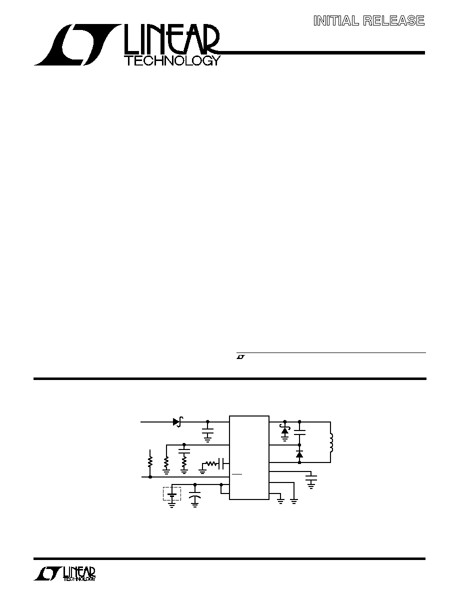
Figure 1. Compact Li-Ion Cellular Phone Charger (0.8A)
SW
V
CC
PROG
6.19k
100k
V
IN
8.2V
TO 20V
CHARGE
COMPLETE
+
1571 F01
C1
0.22
µ
F
C
IN
*
10
µ
F
L1**
10
µ
H
LT1571-5
D1
MBRM120T3
D3
MBRM120T3
V
DD
D2
MMBD914L
SELECT
SENSE
GND
CAP
4.2V
Li-Ion
BATTERY
0.33
µ
F
0.1
µ
F
1k
1
µ
F
TOKIN OR MARCON CERAMIC SURFACE MOUNT
COILTRONICS TP3-100, 10
µ
H, 2.2mm HEIGHT (0.8A CHARGING CURRENT)
COILTRONICS TP1 SERIES, 10
µ
H, 1.8mm HEIGHT (<0.5A CHARGING CURRENT)
PANASONIC EEFCD1B220
*
**
***
BOOST
C
OUT
***
22
µ
F
+
V
C
BAT
BAT2
FLAG
300
Final Electrical Specifications
Information furnished by Linear Technology Corporation is believed to be accurate and reliable.
However, no responsibility is assumed for its use. Linear Technology Corporation makes no represen-
tation that the interconnection of its circuits as described herein will not infringe on existing patent rights.
FEATURES
DESCRIPTIO
U
APPLICATIO S
U
TYPICAL APPLICATIO
U
2
LT1571 Series
Supply Voltage (V
CC
) .............................................. 28V
BOOST Pin Voltage with Respect to V
CC
................. 20V
FLAG Pin Voltage ..................................................... V
CC
I
BAT
(Average) ........................................................ 1.5A
Switch Current (Peak) .............................................. 2A
Storage Temperature Range ................. 65
°
C to 150
°
C
Operating Ambient
Temperature Range (Note 2) .................. 40
°
C to 85
°
C
Operating Junction
Temperature Range .............................. 40
°
C to 125
°
C
Lead Temperature (Soldering, 10 sec).................. 300
°
C
Consult factory for Industrial and Military grade parts.
* V
CC1
AND V
CC2
SHOULD BE CONNECTED
TOGETHER CLOSE TO THE PINS
** FOUR CORNER PINS ARE FUSED TO
INTERNAL DIE ATTACH PADDLE FOR
HEAT SINKING. CONNECT THESE FOUR
PINS TO EXPANDED PC LANDS FOR
PROPER HEAT SINKING
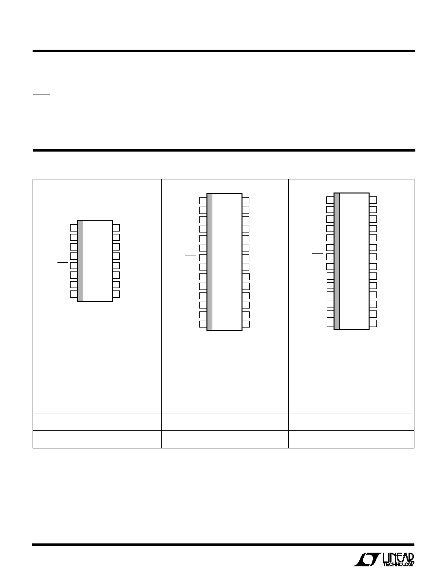
LT1571EGN-1
ORDER PART NUMBER
T
JMAX
= 125
°
C,
JA
= 40
°
C/ W
TOP VIEW
GN PACKAGE
16-LEAD NARROW PLASTIC SSOP
1
2
3
4
5
6
7
8
16
15
14
13
12
11
10
9
**GND
SW
BOOST
BAT2
FLAG
SELECT
SENSE
**GND
GND**
V
CC1
*
V
CC2
*
CAP
PROG
V
C
BAT
GND**
1
2
3
4
5
6
7
8
9
10
11
12
13
14
TOP VIEW
GN PACKAGE
28-LEAD NARROW PLASTIC SSOP
28
27
26
25
24
23
22
21
20
19
18
17
16
15
**GND
**GND
**GND
SW
BOOST
BAT2
FLAG
NC
SELECT
SENSE
**GND
**GND
**GND
**GND
GND**
GND**
GND**
GND**
V
CC1
*
V
CC2
*
CAP
PROG
V
C
BAT
GND**
GND**
GND**
GND**
1
2
3
4
5
6
7
8
9
10
11
12
13
14
TOP VIEW
GN PACKAGE
28-LEAD NARROW PLASTIC SSOP
28
27
26
25
24
23
22
21
20
19
18
17
16
15
**GND
**GND
**GND
SW
BOOST
NC
FLAG
NC
V
FB
SENSE
**GND
**GND
**GND
**GND
GND**
GND**
GND**
GND**
V
CC1
*
V
CC2
*
CAP
PROG
V
C
BAT
GND**
GND**
GND**
GND**
* V
CC1
AND V
CC2
SHOULD BE CONNECTED TOGETHER
CLOSE TO THE PINS
** ALL GND PINS ARE FUSED TO INTERNAL DIE ATTACH
PADDLE FOR HEAT SINKING. CONNECT THESE PINS TO
EXPANDED PC LANDS FOR PROPER HEAT SINKING
40
°
C/W THERMAL RESISTANCE ASSUMES AN INTERNAL
GROUND PLANE DOUBLING AS A HEAT SPREADER
T
JMAX
= 125
°
C,
JA
= 40
°
C/ W
* V
CC1
AND V
CC2
SHOULD BE CONNECTED TOGETHER
CLOSE TO THE PINS
** ALL GND PINS ARE FUSED TO INTERNAL DIE ATTACH
PADDLE FOR HEAT SINKING. CONNECT THESE PINS TO
EXPANDED PC LANDS FOR PROPER HEAT SINKING
40
°
C/W THERMAL RESISTANCE ASSUMES AN INTERNAL
GROUND PLANE DOUBLING AS A HEAT SPREADER
ORDER PART NUMBER
ORDER PART NUMBER
T
JMAX
= 125
°
C,
JA
= 75
°
C/ W
LT1571EGN-2
LT1571EGN-5
(Note 1)
ABSOLUTE AXI U RATI GS
W
W
W
U
PACKAGE/ORDER I FOR ATIO
U
U
W
3
LT1571 Series
The
q
denotes specifications which apply over the full operating temperature range, otherwise specifications are TA = 25
°
C.
V
CC
= 16V (LT1571-1, LT1571-2), V
CC
= 10V (LT1571-5), V
BAT
= 8V (LT1571-1,LT1571-2), V
BAT
= 4V (LT1571-5), maximum operating
V
CC
= V
MAX
= 26V, no load on any outputs unless otherwise noted. (Note 6)
ELECTRICAL CHARACTERISTICS
PARAMETER
CONDITIONS
MIN
TYP
MAX
UNITS
Overall
Supply Current
V
PROG
= 2.7V
q
5.2
7
mA
DC Battery Charging Current, I
BAT
8V
V
CC
26V, 0V
V
BAT
20V (LT1571-1)
R
PROG
= 4.93k
q
0.93
1.0
1.07
A
R
PROG
= 4.93k, T
J
< 0
°
C
q
0.91
1.09
A
R
PROG
= 3.28k
q
1.35
1.5
1.65
A
R
PROG
= 49.3k
75
100
125
mA
R
PROG
= 49.3k, T
J
< 0
°
C
70
130
mA
V
CC
= 26V, V
BAT
= 20V (LT1571-1)
R
PROG
= 4.93k
q
0.93
1.0
1.07
A
Shutdown
Auto Shutdown, Reverse Current from Battery
V
BAT
20V, 0
°
C
T
J
70
°
C (LT1571-1)
q
5
15
µ
A
(When Adapter in Figure 1 Circuit is Removed)
Shutdown Threshold at V
C
Pin
40
80
mV
When V
CC
is Connected
Shutdown Supply Current
V
C
40mV
0.15
0.3
mA
Reference
Reference Voltage (LT1571-1)
R
PROG
= 4.93k. Measured at V
FB
, with VA
Supplying I
PROG
and Switch Off
8V
V
CC
26V, 0
°
C
T
J
70
°
C
q
2.446
2.465
2.480
V
8V
V
CC
26V, 0
°
C
T
J
125
°
C
q
2.441
2.465
2.489
V
8V
V
CC
26V, T
J
< 0
°
C (Note 5)
q
2.430
2.465
2.480
V
Preset Battery Voltage
LT1571-2: 8.2V/8.4V
R
PROG
= 4.93k. Measured at BAT2 Pin
LT1571-5: 4.1V/4.2V
T
J
= 25
°
C
0.5
%
8V
V
CC
26V, 0
°
C
T
J
125
°
C
q
1
1
%
Voltage Setting Resistors Tolerance (R4, R5)
Absolute Value, Not Matching
40
40
%
BAT2 Pin Input Current (LT1571-2, LT1571-5)
V
BAT2
= V
PRESET
1V
q
6
µ
A
Charge Completion Flag (Comparator E6)
Charge Completion Threshold (Note 8)
R
PROG
= 4.93k
0.14
0.20
0.28
A
R
PROG
= 4.93k, R
CAP
= 65.6k
0.05
0.085
0.13
A
Threshold on CAP Pin
Low-to-High Threshold
4
4.5
V
High-to-Low Threshold
0.6
V
FLAG (Open Collector) Output Low
V
CAP
= 4.5V, I
FLAG
1mA
q
0.3
V
FLAG Pin Leakage Current
V
CAP
= 0.6V, V
CC
= 26V
q
3
µ
A
Voltage Amplifier VA
Transconductance
Output Current from 100
µ
A to 500
µ
A
0.3
0.6
2.5
mho
Output Source Current
V
PROG
= V
REF
, V
FB
= V
REF
+ 10mV
1.3
mA
V
FB
Input Bias Current (LT1571-1)
At 0.75mA Output Current
q
±
3
±
15
nA
Overall
Minimum Input Operating Voltage
Undervoltage Lockout
q
6.2
7
7.8
V
Boost Pin Current
V
CC
V
BOOST
20V
q
0.10
20
µ
A
20V < V
CC
V
BOOST
26V
q
0.25
30
µ
A
2V
V
BOOST
V
CC
8V (Switch ON)
q
6
11
mA
8V < V
BOOST
V
CC
20V (Switch ON) (LT1571-1)
q
8
14
mA
4
LT1571 Series
Note 1: Absolute Maximum Ratings are those values beyond which the life
of a device may be impaired.
Note 2: The LT1571 is guaranteed to meet performance specifications
from 0
°
C to 70
°
C. Specifications over the 40
°
C to 85
°
C operating
temperature range are assured by design, characterization and correlation
with statistical process controls.
Note 3: Sense resistor R
S1
and package bond wires.
Note 4: Current (
700
µ
A) flows into the pins during normal operation and
also when an external shutdown signal on the V
C
pin is greater than 0.3V.
Current decreases to
200
µ
A and flows out of the pins when external
shutdown holds the V
C
pin below 0.3V but above shutdown threshold.
Current drops to near zero when input voltage collapses. See External
Shutdown in Applications Information section.
The
q
denotes specifications which apply over the full operating temperature range, otherwise specifications are TA = 25
°
C.
V
CC
= 16V (LT1571-1, LT1571-2), V
CC
= 10V (LT1571-5), V
BAT
= 8V (LT1571-1,LT1571-2), V
BAT
= 4V (LT1571-5), maximum operating
V
CC
= V
MAX
= 26V, no load on any outputs unless otherwise noted. (Note 6)
Note 5: A linear interpolation can be used for reference voltage
specification between 0
°
C and 40
°
C.
Note 6: Maximum allowable ambient temperature may be limited by power
dissipation. Parts may not necessarily be operated simultaneously at
maximum power dissipation and maximum ambient temperature.
Temperature rise calculations must be done as shown in the Applications
Information section to ensure that maximum junction temperature does
not exceed the 125
°
C limit. With high power dissipation, maximum
ambient temperature may be less than 70
°
C.
Note 7: 91% maximum duty cycle is guaranteed by design if V
BAT
or V
X
(see Figure 7 in Application Information) is kept between 3V and 5V.
Note 8: See "Lithium-Ion Charging Completion" in the Applications
Information section.
ELECTRICAL CHARACTERISTICS
PARAMETER
CONDITIONS
MIN
TYP
MAX
UNITS
Switch
Switch ON Resistance
I
SW
= 1.5A, V
BOOST
V
SW
2V
q
0.3
0.5
I
SW
= 1A, V
BOOST
V
SW
< 2V (Unboosted)
q
2.0
I
BOOST
/
I
SW
During Switch ON
V
BOOST
= (V
CC
+ 8V), I
SW
1A
20
35
mA/A
Switch OFF Leakage Current
V
SW
= 0V, V
CC
20V
2
100
µ
A
V
SW
= 0V, 20V < V
CC
26V
4
200
µ
A
Maximum V
BAT
with Switch ON
q
V
CC
2
V
Minimum I
PROG
for Switch ON
1
4
27
µ
A
Minimum I
PROG
for Switch OFF
q
1
2.4
mA
Current Sense Amplifier Inputs (SENSE, BAT)
Sense Resistance (R
S1
)
0.08
0.12
Total Resistance from SENSE to BAT (Note 3)
0.2
0.25
BAT Bias Current (Note 4)
V
C
< 0.3V
200
375
µ
A
V
C
> 0.6V
q
700
1300
µ
A
V
C
< 40mV
5
µ
A
Oscillator
Switching Frequency
LT1571-1, LT1571-2
180
200
220
kHz
LT1571-5
440
500
550
kHz
Switching Frequency Tolerance
All Conditions of V
CC
, Temperature,
LT1571-1, LT1571-2
q
170
200
230
kHz
LT1571-1, LT1571-2, T
J
< 0
°
C
q
160
230
kHz
LT1571-5
q
425
500
575
kHz
LT1571-5, T
J
< 0
°
C
q
400
575
kHz
Maximum Duty Cycle
LT1571-1, LT1571-2
q
87
%
LT1571-1, LT1571-2, T
A
= 25
°
C (Note 7)
90
93
%
LT1571-5
q
77
81
%
Current Amplifier (CA2)
Transconductance
V
C
= 1V, I
VC
=
±
1
µ
A
125
210
550
µ
mho
Maximum V
C
for Switch OFF
q
0.6
V
I
VC
Current (Out of Pin)
V
C
0.6V
100
µ
A
0.2V < V
C
< 0.45V
3
mA
V
C
< 40mV (Shutdown)
300
µ
A

5
LT1571 Series
GND: Ground Pin.
SW: NPN Power Switch Emitter. The Schottky catch diode
must be placed with very short lead length in close
proximity to SW pin and GND.
V
CC1,
V
CC2
: Input Supply. For good bypass, a low ESR
capacitor of 10
µ
F or higher is required, with the lead length
kept to a minimum. V
CC
should be between 8V and 26V
and at least 2V higher than V
BAT
for V
BAT
less than 10V, and
2.5V higher than V
BAT
for V
BAT
greater than 10V. Under-
voltage lockout starts and switching stops when V
CC
goes
below 7V (typical). Note that there is an internal parasitic
diode from SW pin to V
CC
pin. Do not force V
CC
below SW
by more than 0.7V with battery present. All V
CC
pins
should be shorted together close to the pins.
BOOST: This pin is used to bootstrap and drive the NPN
switch to a low on-voltage for low power dissipation. V
BOOST
= V
CC
+ V
BAT
when switch is on. For less power dissipation
use V
BOOST
= 3V to 6V (see Applications Information).
SENSE: Current Amplifier CA1 Input. Sensing can be at
either terminal of the battery. Note that current sense
resistor R
S1
(0.08
) is between SENSE and BAT pins.
BAT: Current Amplifier CA1 Input.
BAT2 (LT1571-2, LT1571-5): This pin is used to connect
the battery to the internal preset voltage setting resistor.
An internal switch disconnects the internal divider from
the battery when the device is in shutdown or when input
power is disconnected. This disconnect function
eliminates current drain due to the resistor divider. This
pin should be connected to the positive node of the
battery if the internal preset divider is used. Otherwise
this pin should be grounded. Maximum voltage on this
pin is 20V.
PROG: This pin is for programming the charge current
and for system loop compensation. Charge current is
regulated to 2000
×
the current drawn from the PROG
pin. During normal operation, V
PROG
stays close to
2.465V. If it is shorted to GND, switching will stop. When
a microprocessor-controlled DAC is used to program
charge current, it must be capable of sinking current at a
compliance up to 2.465V.
V
C
: This is the inner loop control signal of the current mode
PWM. Switching starts at 0.9V. In normal operation, a
higher V
C
corresponds to a higher charge current. A
capacitor of at least 0.1
µ
F to GND filters out noise and
controls the rate of soft-start. To shut down switching, pull
this pin below 0.6V. Typical current out of this pin is 60
µ
A.
When V
C
is pulled below 40mV, LT1571 supply current
drops to typical 150
µ
A.
SELECT (LT1571-2, LT1571-5): This pin is used to select
the preset battery voltage. For the LT1571-2, leave this pin
open for 8.2V and ground it for 8.4V. For the LT1571-5,
leave this pin open for 4.1V and ground it for 4.2V. For
other battery voltages, use the adjustable LT1571-1.
V
FB
(LT1571-1): This is the input to the amplifier VA (see
Block Diagram) with a threshold of 2.465V. Typical input
current is about 3nA. When charging batteries, VA moni-
tors the battery voltage and reduces charging current
when battery voltage reaches the preset value. If it is not
used (constant-current only mode), the V
FB
pin should be
grounded.
CAP: A 0.1
µ
F capacitor from CAP to ground is needed to
filter the sampled charge current signal. This filtered
signal is used to set the FLAG pin when the charge current
drops to 20% of the programmed maximum charge cur-
rent. This threshold level can be set as low as 7.5% of the
programmed maximum charge current by adding a resis-
tor on the CAP pin.
FLAG: This pin is an open-collector output that is used to
indicate end of charge. The FLAG pin is driven low when
the charge current drops below a certain percentage of the
programmed charge current as explained in the CAP pin
function. A pull-up resistor is required if this function is
used. This pin is capable of sinking at least 1mA. Maxi-
mum voltage on this pin is V
CC
.
U
U
U
PI FU CTIO S