1573fa.pm6
1
LT1573
Low Dropout
PNP Regulator Driver
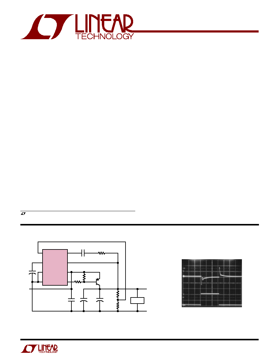
Figure 1. 3.3V, 5A Microprocessor Supply
s
Low Cost Solution for High Current, Low Dropout
Regulators
s
Fast Transient Response Needs Much Less
Bulk Capacitance
s
Latching Overload Protection Minimizes
Heat Sink Size
s
Precision Output Voltage (1%)
s
Single Supply Operation: V
IN
= 2.8V to 10V
s
Small Surface Mount Package
s
Capable of Very Low Dropout Voltage (<0.2V)
s
Fixed or Adjustable Outputs
s
Shutdown
s
3.3V to 2.5V Regulators
s
Microprocessor Power Sources
s
Post Regulator for Switching Supplies
s
High Efficiency Linear Regulators
s
Ultralow Dropout Regulators
s
Low Voltage Linear Regulators
The LT
�
1573 is a regulator driver IC designed to provide
a low cost solution for applications requiring high current,
low dropout and fast transient response. When combined
with an external PNP power transistor, this device pro-
vides load current up to 5A with dropout voltages as low
as 0.35V. The LT1573 circuitry is designed for extremely
fast transient response. This greatly reduces bulk storage
capacitance when the regulator is used in applications
with fast, high current load transients.
To keep cost and complexity low, the LT1573 uses a new
time-delayed latching overcurrent protection technique
that requires no external current sense resistor. Base drive
is limited for instantaneous protection, and a time-delayed
latch protects the regulator from continuous short
circuits.
The LT1573 is available as an adjustable regulator with an
output range of 1.27V to 6.8V and with fixed output
voltages of 2.5V, 2.8V and 3.3V. Output accuracy is better
than 1% to meet the critical regulation requirement of fast
microprocessors. A special 8-pin, fused-lead surface mount
package is used to minimize regulator footprint and pro-
vide adequate heat sinking.
, LTC and LT are registered trademarks of Linear Technology Corporation.
COMP
V
OUT
V
IN
DRIVE
FB
LATCH
SHDN
GND
LT1573
+
C
TIME
C
OUT2
220
�
F
TANT
C
OUT1
1
�
F
CER
�
24
C
C
100pF
V
IN
5V
R
C
1k
R
D
24
V
OUT
3.3V
GND
1573 F01
R
B
50
R1
1.6k
R2
1k
LOAD
+
+
Q
OUT
MOTOROLA
D45H11
V
OUT
= 1.265V (1 + R1/R2)
FOR T < 45
�
C, C
OUT1
= 24
�
1
�
F Y5V CERAMIC SURFACE MOUNT CAPACITORS.
FOR T > 45
�
C, C
OUT1
= 24
�
1
�
F X7R CERAMIC SURFACE MOUNT CAPACITORS.
PLACE C
OUT1
IN THE MICROPROCESSOR SOCKET CAVITY
C
IN
100
�
F
TANT
Transient Response for
0.2A to 5A Output Load Step
10
�
s/DIV
1573 F01a
50mV/DIV
2.5A/DIV
FEATURES
DESCRIPTIO
U
APPLICATIO S
U
TYPICAL APPLICATIO
U
2
LT1573
ORDER PART
NUMBER
S8 PART MARKING
157333
1573I
1573
157325
157328
Consult factory for Military grade parts.
The
q
denotes specifications that apply over the full operating temperature
range, otherwise specifications are at T
A
= 25
�
C. V
IN
= 5V, V
DRIVE
= 3V, unless otherwise noted.
(Note 1)
Input Pin Voltage (V
IN
to GND) ............................... 10V
Drive Pin Voltage (V
DRIVE
to GND) .......................... 10V
Output Pin Voltage (V
OUT
to GND) .......................... 10V
Shutdown Pin Voltage (V
SHDN
to GND) .................. 10V
Operating Junction Temperature Range
LT1573C ............................................... 0
�
C to 125
�
C
LT1573I ............................................ �40
�
C to 125
�
C
Storage Temperature Range ................ � 65
�
C to 150
�
C
Lead Temperature (Soldering, 10 sec.)................ 300
�
C
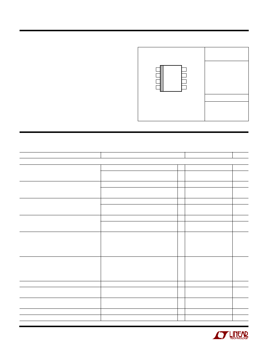
TOP VIEW
COMP
V
OUT
V
IN
DRIVE
FB
LATCH
SHDN
GND
S8 PACKAGE
8-LEAD PLASTIC SO
1
2
3
4
8
7
6
5
T
JMAX
= 125
�
C,
JA
= 85
�
C/ W
LT1573CS8
LT1573CS8-2.5
LT1573CS8-2.8
LT1573CS8-3.3
LT1573IS8
PARAMETER
CONDITIONS
MIN
TYP
MAX
UNITS
DC Characteristics
LT1573 Reference Voltage (Adjustable)(Note 2)
I
DRIVE
= 20mA, T
J
= 25
�
C
1.252
1.265
1.278
V
5mA < I
DRIVE
< 250mA, 3V < V
IN
< 7V,
q
1.225
1.265
1.305
V
1.5V < V
DRIVE
< 7V
LT1573-3.3 Output Voltage (Note 2)
I
DRIVE
= 20mA. T
J
= 25
�
C
3.267
3.3
3.333
V
5mA < I
DRIVE
< 250mA, 3.5V < V
IN
< 7V,
q
3.234
3.3
3.366
V
1.5V < V
DRIVE
< 7V
LT1573-2.8 Output Voltage (Note 2)
I
DRIVE
= 20mA, T
J
= 25
�
C
2.772
2.8
2.828
V
5mA < I
DRIVE
< 250mA, 3V < V
IN
< 7V,
q
2.744
2.8
2.856
V
1.5V < V
DRIVE
< 7V
LT1573-2.5 Output Voltage (Note 2)
I
DRIVE
= 20mA, T
J
= 25
�
C
2.475
2.5
2.525
V
5mA < I
DRIVE
< 250mA, 3V < V
IN
< 7V,
q
2.450
2.5
2.550
V
1.5V < V
DRIVE
< 7V
Line Regulation
LT1573 (V
FB
)
I
DRIVE
= 20mA, 3V < V
IN
< 7V
q
0.17
2
mV
LT1573-3.3 (V
OUT
)
I
DRIVE
= 20mA, 3.5V < V
IN
< 7V
q
0.34
5
mV
LT1573-2.8 (V
OUT
)
I
DRIVE
= 20mA, 3V < V
IN
< 7V
q
0.34
4
mV
LT1573-2.5 (V
OUT
)
I
DRIVE
= 20mA, 3V < V
IN
< 7V
q
0.25
4
mV
Load Regulation
LT1573 (V
FB
)
I
DRIVE
= 20mA to 250mA
q
7
30
mV
LT1573-3.3 (V
OUT
)
I
DRIVE
= 20mA to 250mA
q
18
40
mV
LT1573-2.8 (V
OUT
)
I
DRIVE
= 20mA to 250mA
q
15
34
mV
LT1573-2.5 (V
OUT
)
I
DRIVE
= 20mA to 250mA
q
13
30
mV
FB
Pin Bias Current (Adjustable Only)
V
FB
= 1.265V
q
0.8
5
�
A
DRIVE Pin Current
V
FB
= 1.35V, V
DRIVE
= 7V
q
2
mA
V
FB
= 1.15V, V
DRIVE
= 1.5V
q
250
440
mA
DRIVE Pin Saturation Voltage
I
DRIVE
= 20mA, V
FB
= 1.15V
q
0.12
0.3
V
I
DRIVE
= 250mA, V
FB
= 1.15V
q
0.73
1.4
V
SHDN Pin Threshold Voltage
q
1.0
1.33
1.6
V
SHDN Pin Current
V
SHDN
= 5V
200
�
A
ABSOLUTE AXI U RATI GS
W
W
W
U
PACKAGE/ORDER I FOR ATIO
U
U
W
ELECTRICAL CHARACTERISTICS
3
LT1573
PARAMETER
CONDITIONS
MIN
TYP
MAX
UNITS
LATCH Pin Latch-Off Threshold Voltage
q
0.8
1.4
2.2
V
LATCH Pin Charging Current
7
�
A
LATCH Pin Latching Current
0.65
mA
V
IN
� V
OUT
Differential Threshold for Latch Disable
q
0.4
0.7
1.0
V
Input Quiescent Current
V
IN
= 7V
q
1.7
3.5
mA
Minimum Input Voltage for Bias Operation
q
2.8
V
Note 1: Absolute Maximum Ratings are those values beyond which the life
of the device may be impaired.
Note 2: Operating conditions are limited by maximum junction
temperature. The regulated feedback or output voltage specification will
not apply for all possible combinations of input voltage, drive voltage and
drive current. When operating at maximum drive current, the drive voltage
range must be limited. When operating at maximum input and drive
voltage, the drive current must be limited.
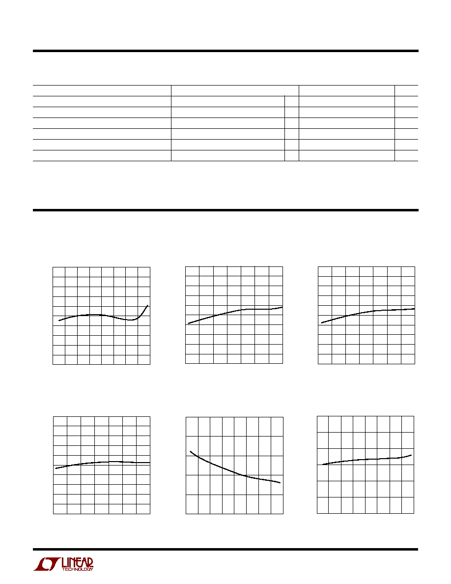
TEMPERATURE (
�
C)
�50
FEEDBACK PIN VOLTAGE (V)
1.290
1.285
1.280
1.275
1.270
1.265
1.260
1.255
1.250
1.245
1.240
0
50
75
1573 G01
�25
25
100 125
150
LT1573 Feedback Pin Voltage
vs Temperature
TEMPERATURE (
�
C)
�50
OUTPUT VOLTAGE (V)
3.40
3.38
3.36
3.34
3.32
3.30
3.28
3.26
3.24
3.22
3.20
0
50
75
1573 G02
�25
25
100
125
LT1573-3.3V Output Voltage
vs Temperature
TEMPERATURE (
�
C)
�50
OUTPUT VOLTAGE (V)
2.90
2.88
2.86
2.84
2.82
2.80
2.78
2.76
2.74
2.72
2.70
0
50
75
1573 G03
�25
25
100
125
LT1573-2.8V Output Voltage
vs Temperature
TEMPERATURE (
�
C)
QUIESCENT CURRENT (mA)
1573 G06
3.0
2.5
2.0
1.5
1.0
0.5
0
�50
0
50
75
�25
25
100 125
150
LT1573-2.5V Output Voltage
vs Temperature
TEMPERATURE (
�
C)
�50
OUTPUT VOLTAGE (V)
2.60
2.58
2.56
2.54
2.52
2.50
2.48
2.46
2.44
2.42
2.40
0
50
75
1573 G04
�25
25
100
125
Feedback Pin Bias Current
vs Temperature
Quiescent Current
vs Temperature
TEMPERATURE (
�
C)
�50
FEEDBACK PIN CURRENT (
�
A)
2.5
2.0
1.5
1.0
0.5
0
0
50
75
1573 G05
�25
25
100 125
150
The
q
denotes specifications that apply over the full operating temperature
range, otherwise specifications are at T
A
= 25
�
C. V
IN
= 5V, V
DRIVE
= 3V, unless otherwise noted.
ELECTRICAL CHARACTERISTICS
TYPICAL PERFOR A CE CHARACTERISTICS
U
W
4
LT1573
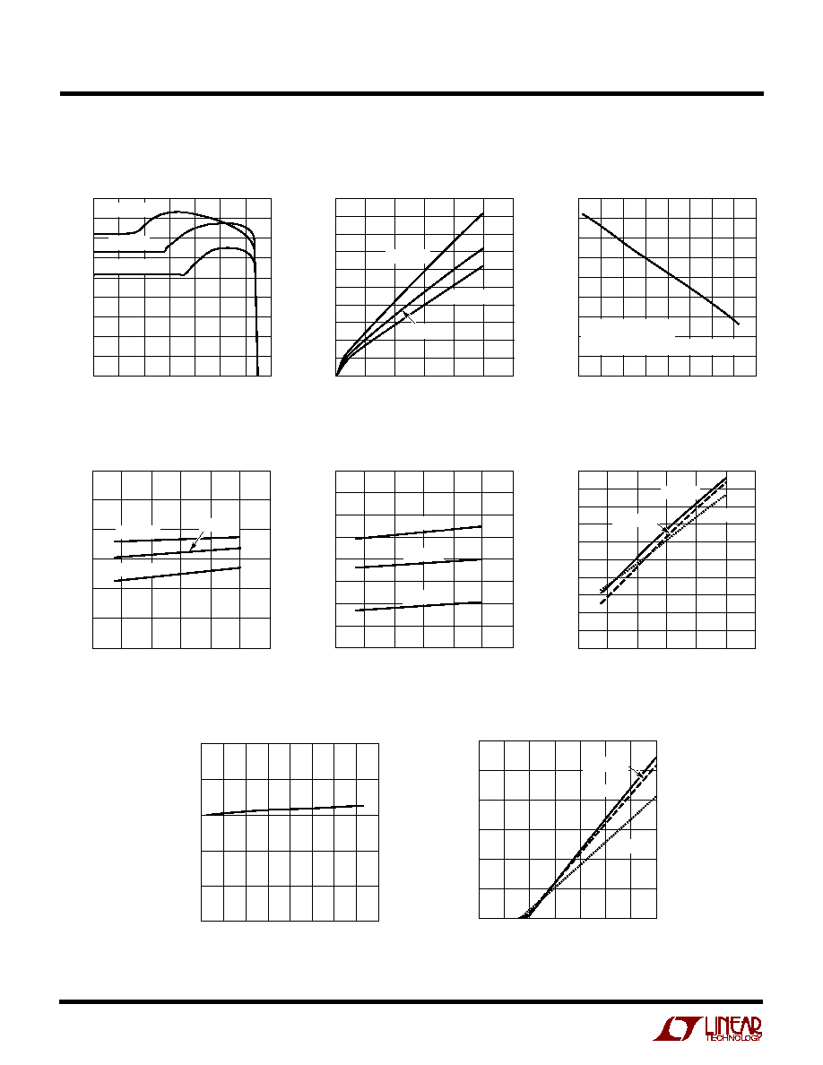
FEEDBACK PIN VOLTAGE (V)
0
DRIVE PIN CURRENT (mA)
1.0
1.2
450
400
350
300
250
200
150
100
50
0
1573 G07
0.4
0.6
0.8
0.2
1.4
T
J
= 130
�
C
T
J
= 25
�
C
T
J
= �45
�
C
Drive Pin Current vs
Feedback Pin Voltage
TEMPERATURE (
�
C)
�50
V
IN
� V
OUT
(V)
150
1573 G09
�25
0
25
50
75
125
100
0.85
0.80
0.75
0.70
0.65
0.60
0.55
0.50
0.45
0.40
V
IN
= 5V
LATCH DISABLED FOR
(V
IN
� V
OUT
) < LATCH DISABLE THRESHOLD
DRIVE PIN CURRENT (mA)
0
DRIVE PIN VOLTAGE (V)
50
100
150
200
1573 G08
250
1.0
0.9
0.8
0.7
0.6
0.5
0.4
0.3
0.2
0.1
0
300
T
J
= 130
�
C
T
J
= �45
�
C
T
J
= 25
�
C
Latch-Disable Threshold
(V
IN
� V
OUT
) vs Temperature
INPUT VOLTAGE (V)
2
3
LATCH PIN LATCH-OFF THRESHOLD (V)
3.0
2.5
2.0
1.5
1.0
0.5
0
4
5
7
6
1573 G10
8
T
J
= 125
�
C
T
J
= �45
�
C
T
J
= 25
�
C
Latch Charging Current vs
Input Voltage
Latch Pin Latch-Off Threshold vs
Input Voltage
INPUT VOLTAGE (V)
2
LATCHING CURRENT (mA)
1.0
0.9
0.8
0.7
0.6
0.5
0.4
0.3
0.2
0.1
0
4
5
7
3
6
1573 G12
8
T
J
= 25
�
C
T
J
= �45
�
C
T
J
= 125
�
C
Latching Current vs Input Voltage
INPUT VOLTAGE (V)
2
3
5
7
LATCH CHARGING CURRENT (
�
A)
16
14
12
10
8
6
4
2
0
4
6
1573 G11
8
T
J
= 125
�
C
T
J
= 25
�
C
T
J
= �45
�
C
SHUTDOWN PIN VOLTAGE (V)
0
SHUTDOWN PIN CURRENT (
�
A)
300
250
200
150
100
50
0
2
3
5
7
1
4
6
1573 G14
T
J
= 125
�
C
T
J
= 25
�
C
T
J
= �45
�
C
TEMPERATURE (
�
C)
SHUTDOWN THRESHOLD (V)
1.5
1.4
1.3
1.2
1.1
1.0
1573 G13
�50
150
�25
0
25
50
75
125
100
Shutdown Pin Current vs
Shutdown Pin Voltage
Shutdown Voltage Threshold vs
Temperature
Drive Pin Saturation Voltage vs
Drive Pin Current
TYPICAL PERFOR A CE CHARACTERISTICS
U
W

5
LT1573
activated by applying a voltage > 1.3V to the SHDN pin. The
output voltage will restart as soon as the SHDN pin is
pulled below the shutdown threshold. If the shutdown/
reset function is not used, the pin should be grounded. The
voltage applied to the SHDN pin can be higher than the
input voltage. When the SHDN pin voltage is higher than
2V, the SHDN pin current increases and is limited by an
internal 20k resistor.
GND (Pin 4): Circuit Ground.
DRIVE (Pin 5): The DRIVE pin is connected to the collector
of the main drive transistor of the LT1573. This drive
transistor sinks the base current of the external PNP
output transistor. A resistor is normally inserted between
the base of the external PNP output transistor and the
DRIVE pin. This resistor is sized to allow the LT1573 to
sink the appropriate amount of base current for a given
application and to activate the overcurrent latch in a fault
condition.
V
IN
(Pin 6): This pin provides power to all internal circuitry
of the LT1573 including bias, start-up, thermal limit, error
amplifier and all overcurrent latch circuitry.
V
OUT
(Pin 7): The V
OUT
pin is the input to comparator C1
shown in Block Diagram. This pin is normally connected
to the output. The comparator C1 is used to disable the
overcurrent latch during start-up when the output transis-
tor is saturated. For fixed voltage devices the top of the
internal resistor divider that sets the output voltage is
connected to this pin.
COMP (Pin 8): A compensation network is inserted
between the V
OUT
and COMP pins to obtain optimal
transient response. Under normal condition, the DC volt-
age of the COMP pin sits at one V
BE
above ground.
FB
(Pin 1): The feedback pin is the inverting input of the
error amplifier. The noninverting input of the error ampli-
fier is internally connected to a 1.265V reference. The error
amplifier will servo the drive to the output transistor, Q
OUT
in Figure 1, to force the voltage at the feedback pin to be
1.265V. Output voltage is set by a resistor divider as
shown in Figure 1. For adjustable devices an external
resistor divider is used to set the output voltage. For fixed
voltage devices the resistor divider is internal and the top
of the resistor divider is connected to the V
OUT
pin.
LATCH (Pin 2): The LT1573 provides overcurrent protec-
tion with a timed latch-off circuit. The latch-off time out is
triggered when the DRIVE pin is pulled below the satura-
tion voltage of the drive transistor. The saturation voltage
is a function of the drive current and is equal to approxi-
mately 130mV at 20mA rising to 780mV at 250mA (see
typical performance curves). The time out is set by the
latch charging current and the value of a capacitor con-
nected between the LATCH pin and ground. If the
overcurrent condition persists at the end of the timing
cycle the regulator will latch off until either the latch is reset
or power is cycled off and back on. The latch can be reset
by either pulling the SHDN pin high, pulling current out of
the LATCH pin greater than latching current or grounding
the LATCH pin. Exceeding the thermal limit temperature
will trigger the latch with no timing delay. Under normal
condition, the DC voltage at the LATCH pin is zero. When
the system is latched off, the DC voltage at theLATCH pin
is two V
BE
above ground.
SHDN (Pin 3): The SHDN pin has two functions. It can be
used to turn off the output voltage by disabling the drive to
the output transistor. It can also be used to reset the
current limit latch. The shutdown/reset functions are
U
U
U
PI FU CTIO S