
1
LT1575/LT1577
Ultrafast Transient Response,
Low Dropout Regulators
Adjustable and Fixed
TYPICAL APPLICATIO
N
U
1
2
3
4
8
7
6
5
SHDN
V
IN
GND
OUT
IPOS
INEG
GATE
COMP
C2
1
µ
F
C5
220
µ
F
5V
GND
1575/77 TA01
V
OUT
3.3V
5A
R2
5
R1
7.5k
12V
LT1575-3.3
C4
1000pF
FOR T > 45
∞
C:
C6 = 24
◊
1
µ
F X7R
CERAMIC SURFACE
MOUNT CAPACITORS.
PLACE C6 IN THE
MICROPROCESSOR
SOCKET CAVITY
FOR T < 45
∞
C:
C6 = 24
◊
1
µ
F Y5V
CERAMIC SURFACE
MOUNT CAPACITORS.
*
Q1
IRFZ24
+
C3
10pF
C6*
24
µ
F
Ultrafast Transient Response 5V to 3.3V Low Dropout Regulator
(For Schematic Including Current Limit, See Typical Applications)
50mV/DIV
2A/DIV
100
µ
s/DIV
1575/77 TA02
Transient Response for
0.2A to 5A Output Load Step
s
Pentium
Æ
Processor Supplies
s
PowerPC
TM
Supplies
s
5V to 3.XXV or 3.3V to 2.XXV Microprocessor Supplies
s
GTL Termination
s
Low Voltage Logic Supplies
LT1575CN8/LT1575CS8
Adjustable
LT1575CN8-1.5/LT1575CS8-1.5
1.5V Fixed
LT1575CN8-2.8/LT1575CS8-2.8
2.8V Fixed
LT1575CN8-3.3/LT1575CS8-3.3
3.3V Fixed
LT1575CN8-3.5/LT1575CS8-3.5
3.5V Fixed
LT1575CN8-5/LT1575CS8-5
5V Fixed
LT1577CS-ADJ/ADJ
Adjustable, Adjustable
LT1577CS-3.3/ADJ
3.3V Fixed, Adjustable
LT1577CS-3.3/2.8
3.3V Fixed, 2.8V Fixed
Consult factory for additional output voltage combinations available
in the LT1577.
APPLICATIO
N
S
U
DESCRIPTIO
N
U
s
UltraFast
TM
Transient Response
Eliminates
Tantalum and Electrolytic Output Capacitors
s
FET R
DS(ON)
Defines Dropout Voltage
s
1% Reference/Output Voltage Tolerance Over
Temperature
s
Typical Load Regulation: 1mV
s
High Side Sense Current Limit
s
Multifunction Shutdown Pin with Latchoff
FEATURES
The LT
Æ
1575/LT1577 are single/dual controller ICs that
drive low cost external N-channel MOSFETs as source
followers to produce ultrafast transient response, low
dropout voltage regulators.
The LT1575/LT1577 achieve unprecedented transient-
load performance by eliminating expensive tantalum or
bulk electrolytic output capacitors in the most demanding
modern microprocessor applications. Precision-trimmed
adjustable and fixed output voltage versions accommo-
date any required microprocessor power supply voltage.
Selection of the N-channel MOSFET R
DS(ON)
allows very
low dropout voltages to be achieved.
Unique protection features include a high side current
limit amplifier that activates a fault protection timer
circuit. A multifunction Shutdown pin provides either
current limit time-out with latchoff, overvoltage protec-
tion, thermal shutdown or a combination of these func-
tions. The LT1575 is available in 8-pin SO or PDIP and the
LT1577 is available in 16-pin narrow body SO.
UltraFast is a trademark of Linear Technology Corporation.
Pentium is a registered trademark of Intel Corporation.
PowerPC is a trademark of IBM Corporation.
, LTC and LT are registered trademarks of Linear Technology Corporation.
2
LT1575/LT1577
A
U
G
W
A
W
U
W
A
R
BSOLUTE
XI
TI
S
(Note 1)
V
IN
, IPOS, INEG ...................................................... 22V
SHDN ....................................................................... V
IN
Operating Ambient Temperature Range ..... 0
∞
C to 70
∞
C
Junction Temperature (Note 2) ................ 0
∞
C to 100
∞
C
Storage Temperature Range ................ ≠ 65
∞
C to 150
∞
C
Lead Temperature (Soldering, 10 sec) ................. 300
∞
C
W
U
U
PACKAGE/ORDER I FOR ATIO
1
2
3
4
8
7
6
5
TOP VIEW
SHDN
V
IN
GND
OUT
IPOS
INEG
GATE
COMP
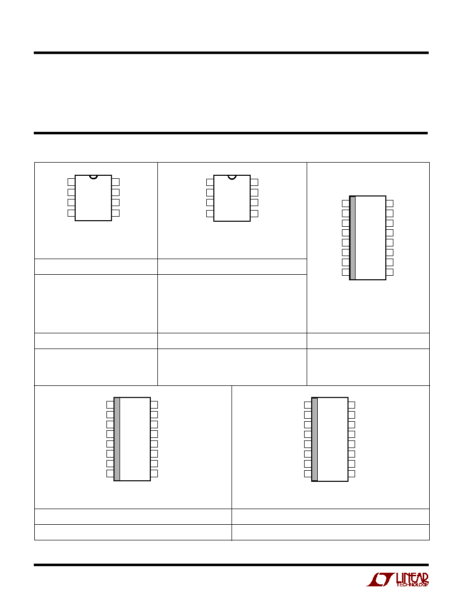
S8 PACKAGE
8-LEAD PLASTIC SO
N8 PACKAGE
8-LEAD PDIP
T
JMAX
= 100
∞
C,
JA
= 100
∞
C/ W (N8)
T
JMAX
= 100
∞
C,
JA
= 130
∞
C/ W (S8)
LT1575CN8-1.5
LT1575CS8-1.5
LT1575CN8-2.8
LT1575CS8-2.8
LT1575CN8-3.3
ORDER PART NUMBER
ORDER PART NUMBER
LT1575CS8-3.3
LT1575CN8-3.5
LT1575CS8-3.5
LT1575CN8-5
LT1575CS8-5
157535
15755
157515
157528
157533
ORDER PART NUMBER
LT1577CS-ADJ/ADJ
T
JMAX
= 100
∞
C,
JA
= 100
∞
C/ W
TOP VIEW
S PACKAGE
16-LEAD PLASTIC NARROW SO
1
2
3
4
5
6
7
8
16
15
14
13
12
11
10
9
SHDN1
V
IN1
GND1
FB1
SHDN2
V
IN2
GND2
FB2
IPOS1
INEG1
GATE1
COMP1
IPOS2
INEG2
GATE2
COMP2
1
2
3
4
8
7
6
5
TOP VIEW
SHDN
V
IN
GND
FB
IPOS
INEG
GATE
COMP
S8 PACKAGE
8-LEAD PLASTIC SO
N8 PACKAGE
8-LEAD PDIP
T
JMAX
= 100
∞
C,
JA
= 100
∞
C/ W (N8)
T
JMAX
= 100
∞
C,
JA
= 130
∞
C/ W (S8)
LT1575CN8
LT1575CS8
1575
S8 PART MARKING
S8 PART MARKING
Consult factory for Industrial and Military grade parts.
ORDER PART NUMBER
LT1577CS-3.3/ADJ
T
JMAX
= 100
∞
C,
JA
= 100
∞
C/ W
TOP VIEW
S PACKAGE
16-LEAD PLASTIC NARROW SO
1
2
3
4
5
6
7
8
16
15
14
13
12
11
10
9
SHDN1
V
IN1
GND1
OUT-3.3
SHDN2
V
IN2
GND2
FB
IPOS1
INEG1
GATE1
COMP1
IPOS2
INEG2
GATE2
COMP2
ORDER PART NUMBER
LT1577CS-3.3/2.8
T
JMAX
= 100
∞
C,
JA
= 100
∞
C/ W
TOP VIEW
S PACKAGE
16-LEAD PLASTIC NARROW SO
1
2
3
4
5
6
7
8
16
15
14
13
12
11
10
9
SHDN1
V
IN1
GND1
OUT-3.3
SHDN2
V
IN2
GND2
OUT-2.8
IPOS1
INEG1
GATE1
COMP1
IPOS2
INEG2
GATE2
COMP2
3
LT1575/LT1577
ELECTRICAL CHARACTERISTICS
T
A
= 25
∞
C, V
IN
= 12V, GATE = 6V, IPOS = INEG = 5V, SHDN = 0.75V unless otherwise noted.
SYMBOL
PARAMETER
CONDITIONS
MIN
TYP
MAX
UNITS
I
Q
Supply Current
q
5
12
19
mA
V
FB
LT1575 Reference Voltage
≠ 0.6
1.210
0.6
%
q
≠ 1.0
1.210
1.0
%
V
OUT
LT1575-1.5 Output Voltage
≠ 0.6
1.500
0.6
%
q
≠ 1.0
1.500
1.0
%
LT1575-2.8 Output Voltage
≠ 0.6
2.800
0.6
%
q
≠ 1.0
2.800
1.0
%
LT1575-3.3 Output Voltage
≠ 0.6
3.300
0.6
%
q
≠ 1.0
3.300
1.0
%
LT1575-3.5 Output Voltage
≠ 0.6
3.500
0.6
%
q
≠ 1.0
3.500
1.0
%
LT1575-5 Output Voltage
≠ 0.6
5.000
0.6
%
q
≠ 1.0
5.000
1.0
%
Line Regulation
10V
V
IN
20V
q
0.01
0.03
%/V
I
FB
FB Input Bias Current
FB = V
FB
q
≠ 0.6
≠ 4.0
µ
A
I
OUT
OUT Divider Current
OUT = V
OUT
q
0.5
1.0
1.5
mA
A
VOL
LT1575 Large-Signal Voltage Gain
V
GATE
= 3V to 10V
q
69
84
dB
LT1575-1.5 Large-Signal Voltage Gain
V
GATE
= 3V to 10V
q
67
82
dB
LT1575-2.8 Large-Signal Voltage Gain
V
GATE
= 3V to 10V
q
60
76
dB
LT1575-3.3 Large-Signal Voltage Gain
V
GATE
= 3V to 10V
q
60
75
dB
LT1575-3.5 Large-Signal Voltage Gain
V
GATE
= 3V to 10V
q
60
74
dB
LT1575-5 Large-Signal Voltage Gain
V
GATE
= 3V to 10V
q
56
71
dB
V
OL
GATE Output Swing Low (Note 3)
I
GATE
= 0mA
q
2.5
3.0
V
V
OH
GATE Output Swing High
I
GATE
= 0mA
q
V
IN
≠ 1.6
V
IN
≠ 1
V
IPOS + INEG Supply Current
3V
IPOS
20V
q
0.3
0.625
1.0
mA
Current Limit Threshold Voltage
42
50
58
mV
q
37
50
63
mV
Current Limit Threshold Voltage
3V
IPOS
20V
q
≠ 0.20
≠ 0.50
%/V
Line Regulation
SHDN Sink Current
Current Flows Into Pin
q
2.5
5.0
8.0
µ
A
SHDN Source Current
Current Flows Out of Pin
q
≠ 8
≠ 15
≠ 23
µ
A
SHDN Low Clamp Voltage
q
0.1
0.25
V
SHDN High Clamp Voltage
q
1.50
1.85
2.20
V
SHDN Threshold Voltage
q
1.18
1.21
1.240
V
SHDN Threshold Hysteresis
q
50
100
150
mV
The
q
denotes specifications which apply over the full operating
temperature range.
Note 1: Absolute Maximum Ratings are those values beyond which the life
of the device may be impaired.
Note 2: T
J
is calculated from the ambient temperature T
A
and power
dissipation P
D
according to the following formulas:
LT1575CN8: T
J
= T
A
+ (P
D
∑ 100
∞
CW)
LT1575CS8: T
J
= T
A
+ (P
D
∑ 130
∞
CW)
LT1577CS: T
J
= T
A
+ (P
D
∑ 100
∞
CW)
Because the LT1577 consists of two regulators in the package, the total
LT1577 power dissipation must be used for its junction temperature
calculation. The total LT1577 P
D
= P
D
(Regulator 1) + P
D
(Regulator 2).
Note 3: The V
GS(th)
of the external MOSFET must be greater than
3V ≠ V
OUT
.
4
LT1575/LT1577
TYPICAL PERFOR
M
A
N
CE CHARACTERISTICS
U
W
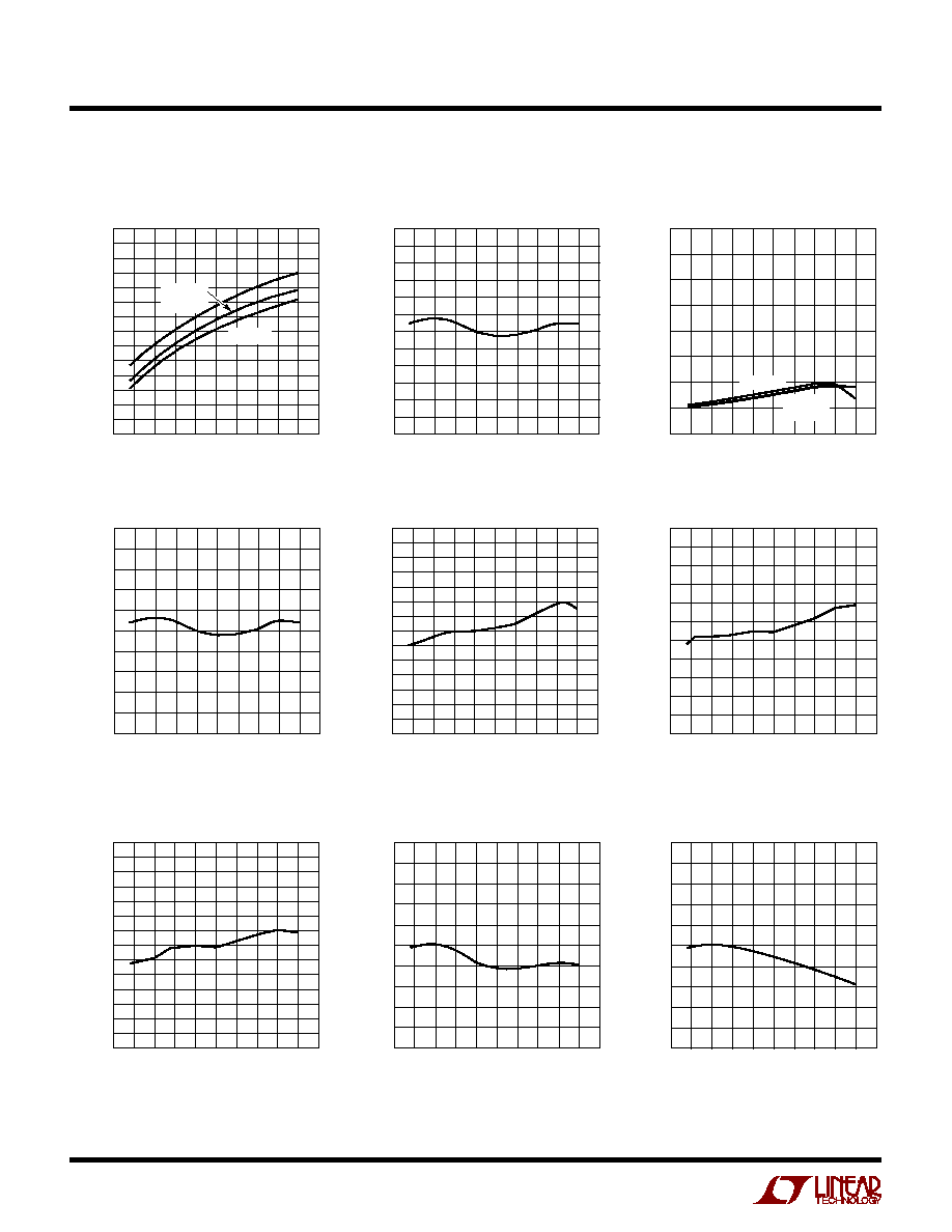
Quiescent Current vs Temperature
FB Input Bias Current
vs Temperature
Adjustable LT1575 V
REF
vs Temperature
TEMPERATURE (
∞
C)
≠75
5
QUIESCENT CURRENT (mA)
7
9
11
19
15
≠25
25 50
150
17
13
6
8
10
18
14
16
12
≠50
0
75 100 125
175
1575/77 G01
V
IN
= 8V
V
IN
= 12V
V
IN
= 20V
TEMPERATURE (
∞
C)
≠75
REFERENCE VOLTAGE (V)
1.210
1.214
1.218
1.222
125
1575/77 G02
1.206
1.202
1.208
1.212
1.216
1.220
1.204
1.200
1.198
≠25
25
75
≠50
150
0
50
100
175
TEMPERATURE (
∞
C)
≠75
FB INPUT BIAS CURRENT (
µ
A)
3.0
4.0
125
1575/77 G03
2.0
1.0
2.5
3.5
1.5
0.5
0
≠25
25
75
≠ 50
150
0
50
100
175
V
IN
= 20V
V
IN
= 12V
V
IN
= 8V
LT1575-3.5 V
OUT
vs Temperature
LT1575-1.5 V
OUT
vs Temperature
LT1575-2.8 V
OUT
vs Temperature
LT1575-3.3 V
OUT
vs Temperature
TEMPERATURE (
∞
C)
≠75
OUTPUT VOLTAGE (V)
3.303
3.315
3.327
3.333
125
1575/77 G06
3.291
3.279
3.297
3.309
3.321
3.285
3.273
3.267
≠25
25
75
≠50
150
0
50
100
175
TEMPERATURE (
∞
C)
≠75
OUT DIVIDER CURRENT (mA)
1.1
1.3
1.5
125
1575/77 G09
0.9
0.7
1.0
1.2
1.4
0.8
0.6
0.5
≠25
25
75
≠ 50
150
0
50
100
175
OUT Divider Current
vs Temperature
TEMPERATURE (
∞
C)
≠75
REFERENCE VOLTAGE (V)
1.503
1.509
1.515
125
1575/77 G04
1.500
1.497
1.494
1.491
1.488
1.485
1.506
1.512
≠25
25
75
≠50
150
0
50
100
175
TEMPERATURE (
∞
C)
≠75
OUTPUT VOLTAGE (V)
2.828
≠25
25 50
150
2.824
2.800
2.816
2.812
2.808
2.804
2.800
2.796
2.792
2.788
2.784
2.780
2.776
2.772
≠50
0
75 100 125
175
1575/77 G05
TEMPERATURE (
∞
C)
≠75
OUTPUT VOLTAGE (V)
3.535
≠25
25 50
150
3.530
3.525
3.520
3.515
3.510
3.505
3.500
3.495
3.490
3.485
3.480
3.475
3.470
3.465
≠50
0
75 100 125
175
1575/77 G07
LT1575-5 V
OUT
vs Temperature
TEMPERATURE (
∞
C)
≠75
OUTPUT VOLTAGE (V)
5.010
5.030
5.050
125
1575/77 G08
4.990
4.970
5.000
5.020
5.040
4.980
4.960
4.950
≠25
25
75
≠50
150
0
50
100
175
5
LT1575/LT1577
TYPICAL PERFOR
M
A
N
CE CHARACTERISTICS
U
W
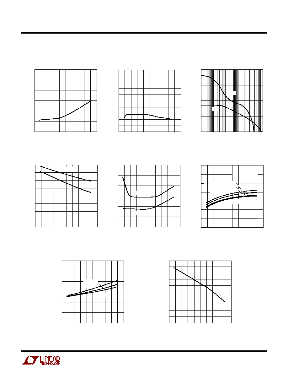
Error Amplifier Large-Signal
Voltage Gain vs Temperature
Gain and Phase vs Frequency
TEMPERATURE (
∞
C)
0
LINE REGULATION (%/
V)
0.010
0.020
0.030
0.005
0.015
0.025
≠25
25
75
125
1575/77 G10
175
≠ 50
≠75
0
50
100
150
V
REF
/V
OUT
Line Regulation
vs Temperature
TEMPERATURE (
∞
C)
≠75
LARGE-SIGNAL VOLTAGE GAIN (dB)
105
115
125
1575/77 G11
95
85
100
110
120
90
80
75
70
≠25
25
75
≠ 50
150
0
50
100
175
Gate Output Swing High
vs Temperature
IPOS + INEG Supply Current
vs Temperature
TEMPERATURE (
∞
C)
≠75
GATE OUTPUT SWING LOW (V)
2.50
3.00
125
1575/77 G13
2.00
1.50
2.25
2.75
1.75
1.25
1.00
≠25
25
75
≠ 50
150
0
50
100
175
I
LOAD
= 50mA
NO LOAD
Gate Output Swing Low
vs Temperature
TEMPERATURE (
∞
C)
0
GATE OUTPUT SWING HIGH (V)
1.0
2.0
3.0
0.5
1.5
2.5
≠25
25
75
125
1575/77 G14
175
≠ 50
≠75
0
50
100
150
NO LOAD
I
LOAD
= 50mA
TEMPERATURE (
∞
C)
≠75
300
I
POS
+ I
NEG
SUPPLY CURRENT (
µ
A)
400
600
700
800
1000
≠ 50
50
100
1575/77 G15
500
900
25
150 175
≠25 0
75
125
IPOS = INEG = 3V
IPOS = INEG = 5V
IPOS = INEG = 12V
IPOS = INEG = 20V
FREQUENCY (Hz)
50
100
ERROR AMPLIFIER GAIN AND PHASE
150
200
1k
100k
1M
100M
1575/77 G12
0
10k
10M
PHASE
GAIN
Current Limit Threshold Voltage
vs Temperature
TEMPERATURE (
∞
C)
35
CURRENT LIMIT THRESHOLD VOLTAGE (mV)
45
55
65
40
50
60
≠25
25
75
125
1575/77 G16
175
≠ 50
≠75
0
50
100
150
IPOS = 5V
IPOS = 3V
IPOS = 20V
Current Limit Threshold Voltage
Line Regulation vs Temperature
TEMPERATURE (
∞
C)
≠75
CURRENT LIMIT THRESHOLD
VOLTAGE LINE REGULATION (%/V)
≠ 0.2
≠ 0.1
0
125
1575/77 G17
≠ 0.3
≠ 0.4
≠ 0.5
≠25
25
75
≠ 50
150
0
50
100
175