
1
LT1575/LT1577
Ultrafast Transient Response,
Low Dropout Regulators
Adjustable and Fixed
TYPICAL APPLICATIO
N
U
1
2
3
4
8
7
6
5
SHDN
V
IN
GND
OUT
IPOS
INEG
GATE
COMP
C2
1
�
F
C5
220
�
F
5V
GND
1575/77 TA01
V
OUT
3.3V
5A
R2
5
R1
7.5k
12V
LT1575-3.3
C4
1000pF
FOR T > 45
�
C:
C6 = 24
�
1
�
F X7R
CERAMIC SURFACE
MOUNT CAPACITORS.
PLACE C6 IN THE
MICROPROCESSOR
SOCKET CAVITY
FOR T < 45
�
C:
C6 = 24
�
1
�
F Y5V
CERAMIC SURFACE
MOUNT CAPACITORS.
*
Q1
IRFZ24
+
C3
10pF
C6*
24
�
F
Ultrafast Transient Response 5V to 3.3V Low Dropout Regulator
(For Schematic Including Current Limit, See Typical Applications)
50mV/DIV
2A/DIV
100
�
s/DIV
1575/77 TA02
Transient Response for
0.2A to 5A Output Load Step
s
Pentium
�
Processor Supplies
s
PowerPC
TM
Supplies
s
5V to 3.XXV or 3.3V to 2.XXV Microprocessor Supplies
s
GTL Termination
s
Low Voltage Logic Supplies
LT1575CN8/LT1575CS8
Adjustable
LT1575CN8-1.5/LT1575CS8-1.5
1.5V Fixed
LT1575CN8-2.8/LT1575CS8-2.8
2.8V Fixed
LT1575CN8-3.3/LT1575CS8-3.3
3.3V Fixed
LT1575CN8-3.5/LT1575CS8-3.5
3.5V Fixed
LT1575CN8-5/LT1575CS8-5
5V Fixed
LT1577CS-ADJ/ADJ
Adjustable, Adjustable
LT1577CS-3.3/ADJ
3.3V Fixed, Adjustable
LT1577CS-3.3/2.8
3.3V Fixed, 2.8V Fixed
Consult factory for additional output voltage combinations available
in the LT1577.
APPLICATIO
N
S
U
DESCRIPTIO
N
U
s
UltraFast
TM
Transient Response
Eliminates
Tantalum and Electrolytic Output Capacitors
s
FET R
DS(ON)
Defines Dropout Voltage
s
1% Reference/Output Voltage Tolerance Over
Temperature
s
Typical Load Regulation: 1mV
s
High Side Sense Current Limit
s
Multifunction Shutdown Pin with Latchoff
FEATURES
The LT
�
1575/LT1577 are single/dual controller ICs that
drive low cost external N-channel MOSFETs as source
followers to produce ultrafast transient response, low
dropout voltage regulators.
The LT1575/LT1577 achieve unprecedented transient-
load performance by eliminating expensive tantalum or
bulk electrolytic output capacitors in the most demanding
modern microprocessor applications. Precision-trimmed
adjustable and fixed output voltage versions accommo-
date any required microprocessor power supply voltage.
Selection of the N-channel MOSFET R
DS(ON)
allows very
low dropout voltages to be achieved.
Unique protection features include a high side current
limit amplifier that activates a fault protection timer
circuit. A multifunction Shutdown pin provides either
current limit time-out with latchoff, overvoltage protec-
tion, thermal shutdown or a combination of these func-
tions. The LT1575 is available in 8-pin SO or PDIP and the
LT1577 is available in 16-pin narrow body SO.
UltraFast is a trademark of Linear Technology Corporation.
Pentium is a registered trademark of Intel Corporation.
PowerPC is a trademark of IBM Corporation.
, LTC and LT are registered trademarks of Linear Technology Corporation.
2
LT1575/LT1577
A
U
G
W
A
W
U
W
A
R
BSOLUTE
XI
TI
S
(Note 1)
V
IN
, IPOS, INEG ...................................................... 22V
SHDN ....................................................................... V
IN
Operating Ambient Temperature Range ..... 0
�
C to 70
�
C
Junction Temperature (Note 2) ................ 0
�
C to 100
�
C
Storage Temperature Range ................ � 65
�
C to 150
�
C
Lead Temperature (Soldering, 10 sec) ................. 300
�
C
W
U
U
PACKAGE/ORDER I FOR ATIO
1
2
3
4
8
7
6
5
TOP VIEW
SHDN
V
IN
GND
OUT
IPOS
INEG
GATE
COMP
S8 PACKAGE
8-LEAD PLASTIC SO
N8 PACKAGE
8-LEAD PDIP
T
JMAX
= 100
�
C,
JA
= 100
�
C/ W (N8)
T
JMAX
= 100
�
C,
JA
= 130
�
C/ W (S8)
LT1575CN8-1.5
LT1575CS8-1.5
LT1575CN8-2.8
LT1575CS8-2.8
LT1575CN8-3.3
ORDER PART NUMBER
ORDER PART NUMBER
LT1575CS8-3.3
LT1575CN8-3.5
LT1575CS8-3.5
LT1575CN8-5
LT1575CS8-5
157535
15755
157515
157528
157533
ORDER PART NUMBER
LT1577CS-ADJ/ADJ
T
JMAX
= 100
�
C,
JA
= 100
�
C/ W
TOP VIEW
S PACKAGE
16-LEAD PLASTIC NARROW SO
1
2
3
4
5
6
7
8
16
15
14
13
12
11
10
9
SHDN1
V
IN1
GND1
FB1
SHDN2
V
IN2
GND2
FB2
IPOS1
INEG1
GATE1
COMP1
IPOS2
INEG2
GATE2
COMP2
1
2
3
4
8
7
6
5
TOP VIEW
SHDN
V
IN
GND
FB
IPOS
INEG
GATE
COMP
S8 PACKAGE
8-LEAD PLASTIC SO
N8 PACKAGE
8-LEAD PDIP
T
JMAX
= 100
�
C,
JA
= 100
�
C/ W (N8)
T
JMAX
= 100
�
C,
JA
= 130
�
C/ W (S8)
LT1575CN8
LT1575CS8
1575
S8 PART MARKING
S8 PART MARKING
Consult factory for Industrial and Military grade parts.
ORDER PART NUMBER
LT1577CS-3.3/ADJ
T
JMAX
= 100
�
C,
JA
= 100
�
C/ W
TOP VIEW
S PACKAGE
16-LEAD PLASTIC NARROW SO
1
2
3
4
5
6
7
8
16
15
14
13
12
11
10
9
SHDN1
V
IN1
GND1
OUT-3.3
SHDN2
V
IN2
GND2
FB
IPOS1
INEG1
GATE1
COMP1
IPOS2
INEG2
GATE2
COMP2
ORDER PART NUMBER
LT1577CS-3.3/2.8
T
JMAX
= 100
�
C,
JA
= 100
�
C/ W
TOP VIEW
S PACKAGE
16-LEAD PLASTIC NARROW SO
1
2
3
4
5
6
7
8
16
15
14
13
12
11
10
9
SHDN1
V
IN1
GND1
OUT-3.3
SHDN2
V
IN2
GND2
OUT-2.8
IPOS1
INEG1
GATE1
COMP1
IPOS2
INEG2
GATE2
COMP2
3
LT1575/LT1577
ELECTRICAL CHARACTERISTICS
T
A
= 25
�
C, V
IN
= 12V, GATE = 6V, IPOS = INEG = 5V, SHDN = 0.75V unless otherwise noted.
SYMBOL
PARAMETER
CONDITIONS
MIN
TYP
MAX
UNITS
I
Q
Supply Current
q
5
12
19
mA
V
FB
LT1575 Reference Voltage
� 0.6
1.210
0.6
%
q
� 1.0
1.210
1.0
%
V
OUT
LT1575-1.5 Output Voltage
� 0.6
1.500
0.6
%
q
� 1.0
1.500
1.0
%
LT1575-2.8 Output Voltage
� 0.6
2.800
0.6
%
q
� 1.0
2.800
1.0
%
LT1575-3.3 Output Voltage
� 0.6
3.300
0.6
%
q
� 1.0
3.300
1.0
%
LT1575-3.5 Output Voltage
� 0.6
3.500
0.6
%
q
� 1.0
3.500
1.0
%
LT1575-5 Output Voltage
� 0.6
5.000
0.6
%
q
� 1.0
5.000
1.0
%
Line Regulation
10V
V
IN
20V
q
0.01
0.03
%/V
I
FB
FB Input Bias Current
FB = V
FB
q
� 0.6
� 4.0
�
A
I
OUT
OUT Divider Current
OUT = V
OUT
q
0.5
1.0
1.5
mA
A
VOL
LT1575 Large-Signal Voltage Gain
V
GATE
= 3V to 10V
q
69
84
dB
LT1575-1.5 Large-Signal Voltage Gain
V
GATE
= 3V to 10V
q
67
82
dB
LT1575-2.8 Large-Signal Voltage Gain
V
GATE
= 3V to 10V
q
60
76
dB
LT1575-3.3 Large-Signal Voltage Gain
V
GATE
= 3V to 10V
q
60
75
dB
LT1575-3.5 Large-Signal Voltage Gain
V
GATE
= 3V to 10V
q
60
74
dB
LT1575-5 Large-Signal Voltage Gain
V
GATE
= 3V to 10V
q
56
71
dB
V
OL
GATE Output Swing Low (Note 3)
I
GATE
= 0mA
q
2.5
3.0
V
V
OH
GATE Output Swing High
I
GATE
= 0mA
q
V
IN
� 1.6
V
IN
� 1
V
IPOS + INEG Supply Current
3V
IPOS
20V
q
0.3
0.625
1.0
mA
Current Limit Threshold Voltage
42
50
58
mV
q
37
50
63
mV
Current Limit Threshold Voltage
3V
IPOS
20V
q
� 0.20
� 0.50
%/V
Line Regulation
SHDN Sink Current
Current Flows Into Pin
q
2.5
5.0
8.0
�
A
SHDN Source Current
Current Flows Out of Pin
q
� 8
� 15
� 23
�
A
SHDN Low Clamp Voltage
q
0.1
0.25
V
SHDN High Clamp Voltage
q
1.50
1.85
2.20
V
SHDN Threshold Voltage
q
1.18
1.21
1.240
V
SHDN Threshold Hysteresis
q
50
100
150
mV
The
q
denotes specifications which apply over the full operating
temperature range.
Note 1: Absolute Maximum Ratings are those values beyond which the life
of the device may be impaired.
Note 2: T
J
is calculated from the ambient temperature T
A
and power
dissipation P
D
according to the following formulas:
LT1575CN8: T
J
= T
A
+ (P
D
� 100
�
CW)
LT1575CS8: T
J
= T
A
+ (P
D
� 130
�
CW)
LT1577CS: T
J
= T
A
+ (P
D
� 100
�
CW)
Because the LT1577 consists of two regulators in the package, the total
LT1577 power dissipation must be used for its junction temperature
calculation. The total LT1577 P
D
= P
D
(Regulator 1) + P
D
(Regulator 2).
Note 3: The V
GS(th)
of the external MOSFET must be greater than
3V � V
OUT
.
4
LT1575/LT1577
TYPICAL PERFOR
M
A
N
CE CHARACTERISTICS
U
W
Quiescent Current vs Temperature
FB Input Bias Current
vs Temperature
Adjustable LT1575 V
REF
vs Temperature
TEMPERATURE (
�
C)
�75
5
QUIESCENT CURRENT (mA)
7
9
11
19
15
�25
25 50
150
17
13
6
8
10
18
14
16
12
�50
0
75 100 125
175
1575/77 G01
V
IN
= 8V
V
IN
= 12V
V
IN
= 20V
TEMPERATURE (
�
C)
�75
REFERENCE VOLTAGE (V)
1.210
1.214
1.218
1.222
125
1575/77 G02
1.206
1.202
1.208
1.212
1.216
1.220
1.204
1.200
1.198
�25
25
75
�50
150
0
50
100
175
TEMPERATURE (
�
C)
�75
FB INPUT BIAS CURRENT (
�
A)
3.0
4.0
125
1575/77 G03
2.0
1.0
2.5
3.5
1.5
0.5
0
�25
25
75
� 50
150
0
50
100
175
V
IN
= 20V
V
IN
= 12V
V
IN
= 8V
LT1575-3.5 V
OUT
vs Temperature
LT1575-1.5 V
OUT
vs Temperature
LT1575-2.8 V
OUT
vs Temperature
LT1575-3.3 V
OUT
vs Temperature
TEMPERATURE (
�
C)
�75
OUTPUT VOLTAGE (V)
3.303
3.315
3.327
3.333
125
1575/77 G06
3.291
3.279
3.297
3.309
3.321
3.285
3.273
3.267
�25
25
75
�50
150
0
50
100
175
TEMPERATURE (
�
C)
�75
OUT DIVIDER CURRENT (mA)
1.1
1.3
1.5
125
1575/77 G09
0.9
0.7
1.0
1.2
1.4
0.8
0.6
0.5
�25
25
75
� 50
150
0
50
100
175
OUT Divider Current
vs Temperature
TEMPERATURE (
�
C)
�75
REFERENCE VOLTAGE (V)
1.503
1.509
1.515
125
1575/77 G04
1.500
1.497
1.494
1.491
1.488
1.485
1.506
1.512
�25
25
75
�50
150
0
50
100
175
TEMPERATURE (
�
C)
�75
OUTPUT VOLTAGE (V)
2.828
�25
25 50
150
2.824
2.800
2.816
2.812
2.808
2.804
2.800
2.796
2.792
2.788
2.784
2.780
2.776
2.772
�50
0
75 100 125
175
1575/77 G05
TEMPERATURE (
�
C)
�75
OUTPUT VOLTAGE (V)
3.535
�25
25 50
150
3.530
3.525
3.520
3.515
3.510
3.505
3.500
3.495
3.490
3.485
3.480
3.475
3.470
3.465
�50
0
75 100 125
175
1575/77 G07
LT1575-5 V
OUT
vs Temperature
TEMPERATURE (
�
C)
�75
OUTPUT VOLTAGE (V)
5.010
5.030
5.050
125
1575/77 G08
4.990
4.970
5.000
5.020
5.040
4.980
4.960
4.950
�25
25
75
�50
150
0
50
100
175
5
LT1575/LT1577
TYPICAL PERFOR
M
A
N
CE CHARACTERISTICS
U
W
Error Amplifier Large-Signal
Voltage Gain vs Temperature
Gain and Phase vs Frequency
TEMPERATURE (
�
C)
0
LINE REGULATION (%/
V)
0.010
0.020
0.030
0.005
0.015
0.025
�25
25
75
125
1575/77 G10
175
� 50
�75
0
50
100
150
V
REF
/V
OUT
Line Regulation
vs Temperature
TEMPERATURE (
�
C)
�75
LARGE-SIGNAL VOLTAGE GAIN (dB)
105
115
125
1575/77 G11
95
85
100
110
120
90
80
75
70
�25
25
75
� 50
150
0
50
100
175
Gate Output Swing High
vs Temperature
IPOS + INEG Supply Current
vs Temperature
TEMPERATURE (
�
C)
�75
GATE OUTPUT SWING LOW (V)
2.50
3.00
125
1575/77 G13
2.00
1.50
2.25
2.75
1.75
1.25
1.00
�25
25
75
� 50
150
0
50
100
175
I
LOAD
= 50mA
NO LOAD
Gate Output Swing Low
vs Temperature
TEMPERATURE (
�
C)
0
GATE OUTPUT SWING HIGH (V)
1.0
2.0
3.0
0.5
1.5
2.5
�25
25
75
125
1575/77 G14
175
� 50
�75
0
50
100
150
NO LOAD
I
LOAD
= 50mA
TEMPERATURE (
�
C)
�75
300
I
POS
+ I
NEG
SUPPLY CURRENT (
�
A)
400
600
700
800
1000
� 50
50
100
1575/77 G15
500
900
25
150 175
�25 0
75
125
IPOS = INEG = 3V
IPOS = INEG = 5V
IPOS = INEG = 12V
IPOS = INEG = 20V
FREQUENCY (Hz)
50
100
ERROR AMPLIFIER GAIN AND PHASE
150
200
1k
100k
1M
100M
1575/77 G12
0
10k
10M
PHASE
GAIN
Current Limit Threshold Voltage
vs Temperature
TEMPERATURE (
�
C)
35
CURRENT LIMIT THRESHOLD VOLTAGE (mV)
45
55
65
40
50
60
�25
25
75
125
1575/77 G16
175
� 50
�75
0
50
100
150
IPOS = 5V
IPOS = 3V
IPOS = 20V
Current Limit Threshold Voltage
Line Regulation vs Temperature
TEMPERATURE (
�
C)
�75
CURRENT LIMIT THRESHOLD
VOLTAGE LINE REGULATION (%/V)
� 0.2
� 0.1
0
125
1575/77 G17
� 0.3
� 0.4
� 0.5
�25
25
75
� 50
150
0
50
100
175

6
LT1575/LT1577
TYPICAL PERFOR
M
A
N
CE CHARACTERISTICS
U
W
SHDN Sink Current
vs Temperature
TEMPERATURE (
�
C)
�75
SHDN SINK CURRENT (
�
A)
5.5
6.5
7.5
125
1575/77 G18
4.5
3.5
5.0
6.0
7.0
4.0
3.0
2.5
�25
25
75
� 50
150
0
50
100
175
SHDN Low Clamp Voltage
vs Temperature
TEMPERATURE (
�
C)
� 75
SHDN LOW CLAMP VOLTAGE (V)
0.15
0.20
0.25
125
1575/77 G20
0.10
0.05
0
� 25
25
75
� 50
150
0
50
100
175
SHDN Source Current
vs Temperature
TEMPERATURE (
�
C)
�75
SHDN SOURCE CURRENT (
�
A)
� 15
� 13
� 11
125
1575/77 G19
� 17
� 19
� 16
� 14
� 12
� 18
� 20
�10
�25
25
75
� 50
150
0
50
100
175
SHDN Hysteresis vs Temperature
TEMPERATURE (
�
C)
�75
SHDN HYSTERESIS (mV)
110
130
150
125
1575/77 G22
90
70
100
120
140
80
60
50
�25
25
75
� 50
150
0
50
100
175
SHDN High Clamp Voltage
vs Temperature
TEMPERATURE (
�
C)
1.5
SHDN HIGH CLAMP VOLTAGE (V)
1.7
1.9
2.1
1.6
1.8
2.0
�25
25
75
125
1575/77 G21
175
� 50
�75
0
50
100
150

7
LT1575/LT1577
PI
N
FU
N
CTIO
N
S
U
U
U
SHDN (Pin 1): This is a multifunction shutdown pin that
provides GATE drive latchoff capability. A 15
�
A current
source, that turns on when current limit is activated,
charges a capacitor placed in series with SHDN to GND
and performs a current limit time-out function. The pin is
also the input to a comparator referenced to V
REF
(1.21V).
When the pin pulls above V
REF
, the comparator latches the
gate drive to the external MOSFET off. The comparator
typically has 100mV of hysteresis and the Shutdown pin
can be pulled low to reset the latchoff function. This pin
provides overvoltage protection or thermal shutdown
protection when driven from various resistor divider
schemes.
V
IN
(Pin 2): This is the input supply for the IC that powers
the majority of internal circuitry and provides sufficient
gate drive compliance for the external N-channel MOSFET.
The typical supply voltage is 12V with 12.5mA of quiescent
current. The maximum operating V
IN
is 20V and the
minimum operating V
IN
is set by V
OUT
+ V
GS
of the
MOSFET at max. I
OUT
+ 1.6V (worst-case V
IN
to GATE
output swing).
GND (Pin 3): Analog Ground. This pin is also the negative
sense terminal for the internal 1.21V reference. Connect
external feedback divider networks that terminate to GND
and frequency compensation components that terminate
to GND directly to this pin for best regulation and perfor-
mance.
FB (Pin 4): This is the inverting input of the error amplifier
for the adjustable voltage LT1575. The noninverting input
is tied to the internal 1.21V reference. Input bias current
for this pin is typically 0.6
�
A flowing out of the pin. This pin
is normally tied to a resistor divider network to set output
voltage. Tie the top of the external resistor divider directly
to the output voltage for best regulation performance.
OUT (Pin 4): This is the inverting input of the error
amplifier for the fixed voltage LT1575. The fixed voltage
parts contain a precision resistor divider network to set
output voltage. The typical resistor divider current is 1mA
into the pin. Tie this pin directly to the output voltage for
best regulation performance.
COMP (Pin 5): This is the high impedance gain node of the
error amplifier and is used for external frequency compen-
sation. The transconductance of the error amplifier is 15
millimhos and open-loop voltage gain is typically 84dB.
Frequency compensation is generally performed with a
series RC network to ground.
GATE (Pin 6): This is the output of the error amplifier that
drives N-channel MOSFETs with up to 5000pF of "effec-
tive" gate capacitance. The typical open-loop output
impedance is 2
. When using low input capacitance
MOSFETs (< 1500pF), a small gate resistor of 2
to 10
dampens high frequency ringing created by an LC reso-
nance that is created by the MOSFET gate's lead induc-
tance and input capacitance. The GATE pin delivers up to
50mA for a few hundred nanoseconds when slewing the
gate of the N-channel MOSFET in response to output load
current transients.
INEG (Pin 7): This is the negative sense terminal of the
current limit amplifier. A small sense resistor is connected
in series with the drain of the external MOSFET and is
connected between the IPOS and INEG pins. A 50mV
threshold voltage in conjunction with the sense resistor
value sets the current limit level. The current sense resis-
tor can be a low value shunt or can be made from a piece
of PC board trace. If the current limit amplifier is not used,
tie the INEG pin to IPOS to defeat current limit. An
alternative is to ground the INEG pin. This action disables
the current limit amplifier and additional internal circuitry
activates the timer circuit on the SHDN pin if the GATE pin
swings to the V
IN
rail. This option provides the user with
a "sense-less" current limit function.
IPOS (Pin 8): This is the positive sense terminal of the
current limit amplifier. Tie this pin directly to the main
input voltage from which the output voltage is regulated.
The typical input voltage is a 5V logic supply. This pin is
also the input to a comparator on the fixed voltage ver-
sions that monitors the input/output differential voltage of
the external MOSFET. If this differential voltage is less than
0.5V, then the SHDN timer is not allowed to start even if the
GATE is at the V
IN
rail. This allows the regulator to start up
normally as the input voltage is ramping up, even with very
slow ramp rates.
8
LT1575/LT1577
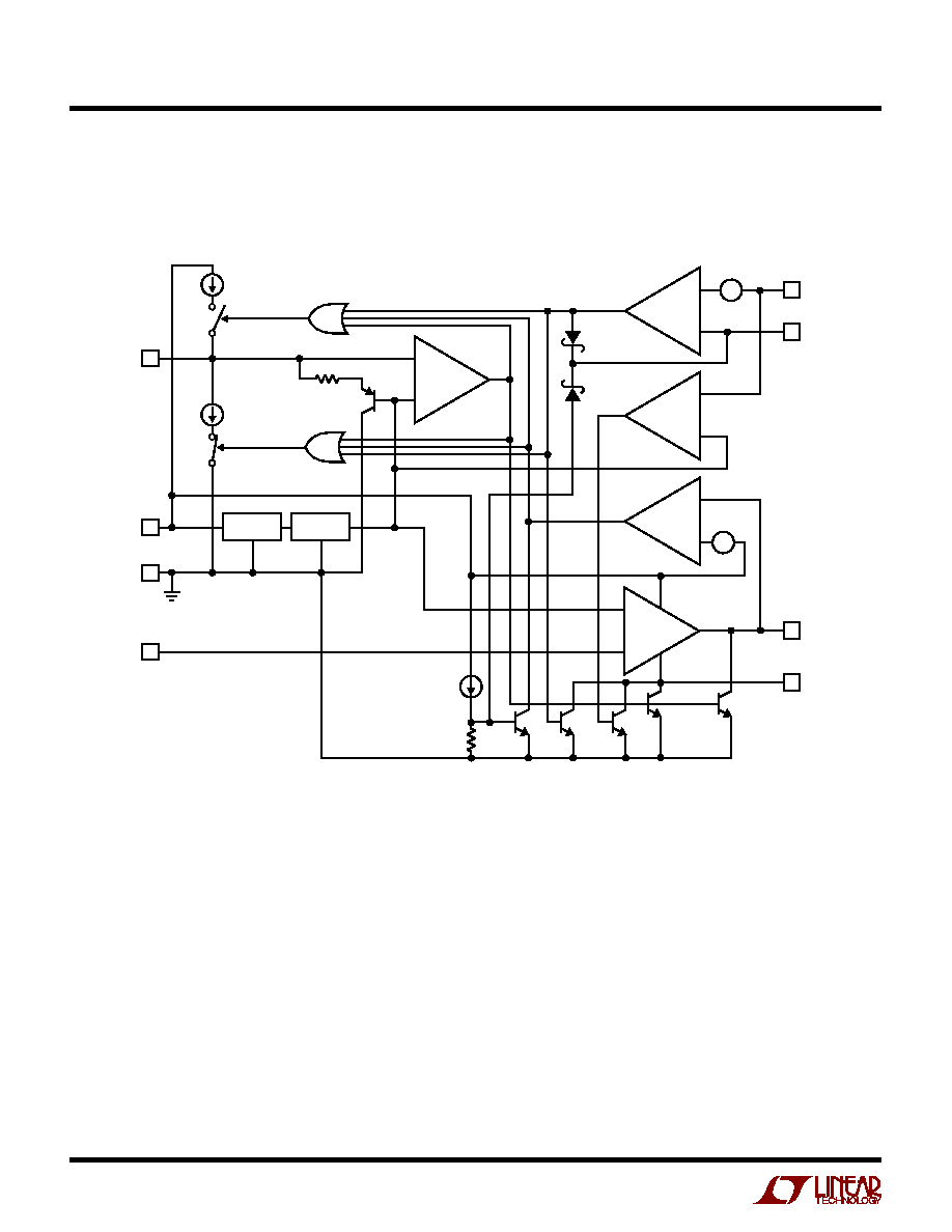
BLOCK DIAGRA
M
W
LT1575 Adjustable Voltage
SW2
NORMALLY
CLOSED
I2
5
�
A
�
+
ERROR AMP
COMP
1575/77 BD1
�
+
COMP1
Q6
SHDN
V
IN
GND
FB
R2
5k
SW1
NORMALLY
OPEN
100mV
HYSTERESIS
I1
15
�
A
I3
100
�
A
�
+
I
LIM
AMP
V
TH1
50mV
+
�
V
TH2
1V
+
�
D1
IPOS
INEG
GATE
D2
�
+
COMP2
�
+
COMP3
OR2
START-UP
V
REF
1.21V
R1
50k
OR1
Q4
Q3
Q2
Q1
Q5

9
LT1575/LT1577
BLOCK DIAGRA
M
W
LT1575 Fixed Voltage
SW2
NORMALLY
CLOSED
I2
5
�
A
�
+
ERROR AMP
COMP
1575/77 BD2
�
+
COMP1
Q6
SHDN
V
IN
GND
OUT
R2
5k
SW1
NORMALLY
OPEN
100mV
HYSTERESIS
I1
15
�
A
I3
100
�
A
�
+
I
LIM
AMP
V
TH1
50mV
+
�
V
TH3
500mV
+
�
V
TH2
1V
+
�
D1
IPOS
INEG
GATE
D2
�
+
�
+
COMP2
COMP4
�
+
COMP3
OR2
START-UP
V
REF
1.21V
R1
50k
OR1
Q4
Q3
Q2
Q1
Q5
R3*
*V
OUT
= (1 + R3/R4)V
REF
R4*
Q7

10
LT1575/LT1577
APPLICATIO
N
S I
N
FOR
M
ATIO
N
W
U
U
U
Introduction
The current generation of microprocessors place strin-
gent demands on the power supply that powers the
processor core. These microprocessors cycle load cur-
rent from near zero to amps in tens of nanoseconds.
Output voltage tolerances as low as
�
100mV include
transient response as part of the specification. Some
microprocessors require only a single output voltage from
which the core and I/O circuitry operate. Other higher
performance processors require a separate power supply
voltage for the processor core and the I/O circuitry. These
requirements mandate the need for very accurate, very
high speed regulator circuits.
Previously employed solutions included monolithic
3-terminal linear regulators, PNP transistors driven by low
cost control circuits and simple buck converter switching
regulators. The 3-terminal regulator achieves a high level
of integration, the PNP driven regulator achieves very low
dropout performance and the switching regulator achieves
high electrical efficiency.
However, the common trait manifested by these solutions
is that transient response is measured in many microsec-
onds. This fact translates to a regulator output decoupling
capacitor scheme that requires several hundred microfar-
ads of very low ESR bulk capacitance using multiple
capacitors surrounding the CPU. This required bulk ca-
pacitance is in addition to the ceramic decoupling capaci-
tor network that handles the transient load response
during the first few hundred nanoseconds as well as
providing microprocessor clock frequency noise immu-
nity. The combined cost of all capacitors is a significant
percentage of the total power supply cost.
The LT1575/LT1577 family of single/dual controller ICs
are unique, easy to use devices that drive external
N-channel MOSFETs as source followers and permit a user
to realize an extremely low dropout, ultrafast transient
response regulator. These circuits achieve superior regu-
lator bandwidth and transient load performance by com-
pletely eliminating expensive tantalum or bulk electrolytic
capacitors in the most modern and demanding micropro-
cessor applications. For example, a 200MHz Pentium
processor can operate with only the recommended 24 1
�
F
ceramic capacitors. Users benefit directly by saving sig-
nificant cost as all additional bulk capacitance is removed.
The additional savings of insertion cost, purchasing/in-
ventory cost and board space are readily apparent.
Precision-trimmed adjustable and fixed output voltage
versions accommodate any required microprocessor
power supply voltage. Proper selection of the N-channel
MOSFET R
DS(ON)
allows user-settable dropout voltage
performance. The only output capacitors required are the
high frequency ceramic decoupling capacitors. This regu-
lator design provides ample bandwidth and responds to
transient load changes in a few hundred nanoseconds
versus regulators that respond in many microseconds.
The ceramic capacitor network generally consists of 10 to
24 1uF capacitors for individual microprocessor require-
ments. The LT1575/LT1577 family also incorporates cur-
rent limiting for no additional system cost, provides on/off
control and overvoltage protection or thermal shutdown
with simple external components.
Therefore, the unique design of these new ICs combines
the benefits of low dropout voltage, high functional inte-
gration, precision performance and ultrafast transient
response, as well as providing significant cost savings on
the output capacitance needed in fast load transient appli-
cations. As lower input/output differential voltage applica-
tions become increasingly prevalent, an LT1575-based
solution achieves comparable efficiency performance with
a switching regulator at an appreciable cost savings.
The new LT1575/LT1577 family of low dropout regulator
controller ICs step to the next level of performance re-
quired by system designers for the latest generation
motherboards and microprocessors. The simple versatil-
ity and benefits derived from these circuits allow the
power supply needs of today's high performance micro-
processors to be met with ease.
Block Diagram Operation
The primary block diagram elements consist of a simple
feedback control loop and the secondary block diagram
elements consist of multiple protection functions. Exam-
ining the block diagram for the LT1575, a start-up circuit
provides controlled start-up for the IC, including the
precision-trimmed bandgap reference, and establishes all
internal current and voltage biasing.

11
LT1575/LT1577
APPLICATIO
N
S I
N
FOR
M
ATIO
N
W
U
U
U
Because the MOSFET pass transistor is connected as a
source follower, the power path gain is much more pre-
dictable than designs that employ a discrete PNP transis-
tor as the pass device. This is due to the significant
production variations encountered with PNP Beta.
MOSFETs are also very high speed devices which enhance
the ability to produce a stable wide bandwidth control
loop. An additional advantage of the follower topology is
inherently good line rejection. Input supply disturbances
do not propagate through to the output. The feedback loop
for a regulator circuit is completed by providing an error
signal to the FB pin in the adjustable voltage version and
the OUT pin in the fixed voltage version. In both cases, a
resistor divider network senses the output voltage and
sets the regulated DC bias point. In general, the LT1575
regulator feedback loop permits a loop crossover fre-
quency on the order of 1MHz while maintaining good
phase and gain margins. This unity-gain frequency is a
factor of 20 to 30 times the bandwidth of currently
implemented regulator solutions for microprocessor power
supplies. This significant performance benefit is what
permits the elimination of all bulk output capacitance.
Several other unique features are included in the design
that increase its functionality and robustness. These func-
tions comprise the remainder of the block diagram.
A high side sense, current limit amplifier provides active
current limiting for the regulator. The current limit ampli-
fier uses an external low value shunt resistor connected in
series with the external MOSFET's drain. This resistor can
be a discrete shunt resistor or can be manufactured from
a Kelvin-sensed section of "free" PC board trace. All load
current flows through the MOSFET drain and thus, through
the sense resistor. The advantage of using high side
current sensing in this topology is that the MOSFET's gain
and the main feedback loop's gain remain unaffected. The
sense resistor develops a voltage equal to I
OUT
(R
SENSE
).
The current limit amplifier's 50mV threshold voltage is a
good compromise between power dissipation in the sense
resistor, dropout voltage impact and noise immunity.
Current limit activates when the sense resistor voltage
equals the 50mV threshold.
Two events occur when current limit activates: the first is
that the current limit amplifier drives Q2 in the block
Reference voltage accuracy for the adjustable version and
output voltage accuracy for the fixed voltage versions are
specified as
�
0.6% at room temperature and as
�
1% over
the full operating temperature range. This places the
LT1575/LT1577 family among a select group of regulators
with a very tightly specified output voltage tolerance. The
accurate 1.21V reference is tied to the noninverting input
of the main error amplifier in the feedback control loop.
The error amplifier consists of a single high gain g
m
stage
with a transconductance equal to 15 millimhos. The
inverting terminal is brought out as the FB pin in the
adjustable voltage version and as the OUT pin in fixed
voltage versions. The g
m
stage provides differential-to-
single ended conversion at the COMP pin. The output
impedance of the g
m
stage is about 1M
and thus, 84dB
of typical DC error amplifier open-loop gain is realized
along with a typical 75MHz uncompensated unity-gain
crossover frequency. Note that the overall feedback
loop's DC gain decreases from the gain provided by the
error amplifier by the attenuation factor in the resistor
divider network which sets the DC output voltage. These
attenuation factors are already built into the Open-Loop
Voltage Gain specifications for the LT1575 fixed voltage
versions in the Electrical Characteristics table to simplify
user calculations. External access to the high impedance
gain node of the error amplifier permits typical loop
compensation to be accomplished with a series RC
network to ground.
A high speed, high current output stage buffers the COMP
node and drives up to 5000pF of "effective" MOSFET gate
capacitance with almost no change in load transient per-
formance. The output stage delivers up to 50mA peak
when slewing the MOSFET gate in response to load
current transients. The typical output impedance of the
GATE pin is typically 2
. This pushes the pole due to the
error amplifier output impedance and the MOSFET input
capacitance well beyond the loop crossover frequency. If
the capacitance of the MOSFET used is less than 1500pF,
it may be necessary to add a small value series gate
resistor of 2
to 10
. This gate resistor helps damp the
LC resonance created by the MOSFET gate's lead induc-
tance and input capacitance. In addition, the pole formed
by this resistance and the MOSFET input capacitance can
be fine tuned.

12
LT1575/LT1577
APPLICATIO
N
S I
N
FOR
M
ATIO
N
W
U
U
U
diagram and clamps the positive swing of the COMP node
in the main error amplifier to a voltage that provides an
output load current of 50mV/R
SENSE
. This action contin-
ues as long as the output current overload persists. The
second event is that a timer circuit activates at the SHDN
pin. This pin is normally held low by a 5
�
A active pull-down
that limits to
100mV above ground. When current limit
activates, the 5
�
A pull-down turns off and a 15
�
A pull-up
current source turns on. Placing a capacitor in series with
the SHDN pin to ground generates a programmable time
ramp voltage.
The SHDN pin is also the positive input of COMP1. The
negative input is tied to the internal 1.21V reference. When
the SHDN pin ramps above V
REF
, the comparator drives
Q4 and Q5. This action pulls the COMP and GATE pins low
and latches the external MOSFET drive off. This condition
reduces the MOSFET power dissipation to zero. The time
period until the latched-off condition occurs is typically
equal to C
SHUT
(1.11V)/15
�
A. For example, a 1
�
F capacitor
on the SHDN pin yields a 74ms ramp time. In short, this
unique circuit block performs a current limit time-out
function that latches off the regulator drive after a pre-
defined time period. The time-out period selected is a
function of system requirements including start-up and
safe operating area. The SHDN pin is internally clamped to
typically 1.85V by Q6 and R2. The comparator tied to the
SHDN pin has 100mV of typical hysteresis to provide
noise immunity. The hysteresis is especially useful when
using the SHDN pin for thermal shutdown.
Restoring normal operation after the load current fault is
cleared is accomplished in two ways. One option is to
recycle the nominal 12V LT1575 supply voltage as long as
an external bleed path for the Shutdown pin capacitor is
provided. The second option is to provide an active reset
circuit that pulls the SHDN pin below V
REF
. Pulling the
SHDN pin below V
REF
turns off the 15
�
A pull-up current
source and reactivates the 5
�
A pull-down. If the SHDN pin
is held below V
REF
during a fault condition, the regulator
continues to operate in current limit into a short. This
action requires being able to sink 15
�
A from the SHDN pin
at less than 1V. The 5
�
A pull-down current source and the
15
�
A pull-up current source are designed low enough in
value so that an external resistor divider network can drive
the SHDN pin to provide overvoltage protection or to
provide thermal shutdown with the use of a thermistor in
the divider network. Diode-ORing these functions to-
gether is simple to accomplish and provides multiple
functionality for one pin.
If the current limit amplifier is not used, two choices
present themselves. The simplest choice is to tie the INEG
pin directly to the IPOS pin. This action defeats current
limit and provides the simplest, no frills circuit. An appli-
cation in which the current limit amplifier is not used is
where an extremely low dropout voltage must be achieved
and the 50mV threshold voltage cannot be tolerated.
However, a second available choice permits a user to
provide short-circuit protection with no external sensing.
This technique is activated by grounding the INEG pin.
This action disables the current limit amplifier because
Schottky diode D1 clamps the amplifier's output and
prevents Q2 from pulling down the COMP node. In addi-
tion, Schottky diode D2 turns off pull-down transistor Q1.
Q1 is normally on and holds internal comparator COMP3's
output low. This comparator circuit, now enabled, moni-
tors the GATE pin and detects saturation at the positive rail.
When a saturated condition is detected, COMP3 activates
the shutdown timer. Once the time-out period occurs, the
output is shut down and latched off. The operation of
resetting the latch remains the same. Note that this tech-
nique does not limit the FET current during the time-out
period. The output current is only limited by the input
power supply and the input/output impedance. Setting the
timer to a short period in this mode of operation keeps the
external MOSFET within its SOA (safe operating area)
boundary and keeps the MOSFET's temperature rise under
control.
Unique circuit design incorporated into the LT1575 allevi-
ates all concerns about power supply sequencing. The
issue of power supply sequencing is an important topic as
the typical LT1575 application has inputs from two sepa-
rate power supply voltages. If the typical 12V V
IN
supply
voltage is slow in ramping up, insufficient MOSFET gate
drive is present and therefore, the output voltage does
not come up. If the V
IN
supply voltage is present, but the
typical 5V supply voltage tied to the IPOS pin has not
started yet, then the feedback loop wants to drive the
GATE pin to the positive V
IN
rail. This would result in a
13
LT1575/LT1577
APPLICATIO
N
S I
N
FOR
M
ATIO
N
W
U
U
U
very large current spike as soon as the 5V supply started
to ramp up. However, undervoltage lockout circuit COMP2,
which monitors the IPOS supply voltage, holds Q3 on and
pulls the COMP pin low until the IPOS voltage increases
to greater than the internal 1.21 reference voltage. The
undervoltage lockout circuit then smoothly releases the
COMP pin and allows the output voltage to come up in
dropout from the input supply voltage. An additional
benefit derived from the speed of the LT1575 feedback
loop is that turn-on overshoot is virtually nonexistent in
a properly compensated system.
An additional circuit feature is built-in to the LT1575 fixed
voltage versions. When the regulator circuit starts up, it
must charge up the output capacitors. The output voltage
typically tracks the input voltage supply as it ramps up with
the difference in input/output voltage defined by the drop-
out voltage. Until the feedback loop comes into regulation,
the circuit operation results in the GATE pin being at the
positive V
IN
rail, which starts the timer at the SHDN pin if
the current limit amplifier is disabled. However, internal
comparator COMP4 monitors the input/output voltage
differential. This comparator does not permit the shut-
down timer to start until the differential voltage is greater
than 500mV. This permits normal start-up to occur.
One final benefit is derived in using an LT1575 fixed
voltage version. Today's highest performance micropro-
cessors dictate that precision resistors must be used with
currently available adjustable voltage regulators to meet
the initial set point tolerance. The LT1575 fixed voltage
versions incorporate the precision resistor divider into the
IC and still maintain a 1% output voltage tolerance over
temperature. Thus, the LT1575 fixed voltage versions
completely eliminate the requirement for precision resis-
tors and this results in additional system cost savings.
Applications Support
Linear Technology invests an enormous amount of time,
resources and technical expertise in understanding, de-
signing and evaluating microprocessor power supply so-
lutions for system designers. As processor speeds and
power increase, the power supply challenges presented to
the motherboard designer increase as well. Application
Note 69, "Using the LT1575 Linear Regulator Controller,"
has been written and serves as an extremely useful guide
for this new family of ICs. This Application Note covers
topics including PC board layout for the LT1575/LT1577
family, MOSFET selection criteria, external component
selection (capacitors) and loop compensation. Linear
Technology welcomes the opportunity to discuss, design,
evaluate and optimize a microprocessor power supply
solution with a customer. For additional information,
consult the factory.
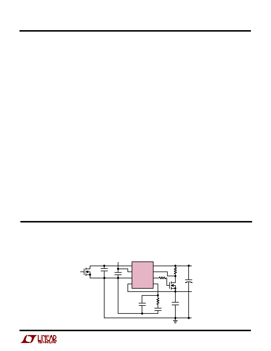
UltraFast Transient Response 5V to 3.5V Low Dropout Regulator
with Current Limit and Timer Latchoff
1
2
3
4
8
7
6
5
SHDN
V
IN
GND
OUT
IPOS
INEG
GATE
COMP
C2
1
�
F
C5
220
�
F
5V
GND
1575/77 TA11
V
OUT
3.5V
5A
R2
5
R3*
0.007
R1
7.5k
12V
LT1575-3.5
C4
1000pF
C1
1
�
F
RESET
R3 IS MADE FROM
"FREE" PC BOARD
TRACE
C6 = 24
�
1
�
F X7R
CERAMIC SURFACE
MOUNT CAPACITORS.
PLACE C6 IN THE
MICROPROCESSOR
SOCKET CAVITY
*
**
Q2
VN2222L
Q1
IRFZ24
+
C3
10pF
C6**
24
�
F
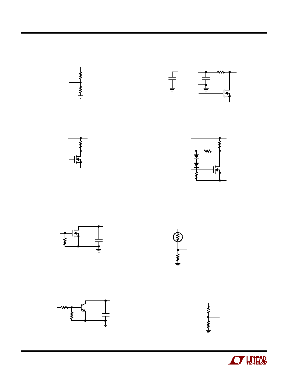
TYPICAL APPLICATIO
N
S
N
U
14
LT1575/LT1577
TYPICAL APPLICATIO
N
S
N
U
Setting Output Voltage with the Adjustable LT1575
FB
1575 TA03
R2
V
OUT
= 1.21V(1 + R2/R1)
V
OUT
R1
Using "Sense-Less" Current Limit
C1
10
�
F
C
T
R3
10
IPOS
SHDN
V
CC
1575 TA04
V
OUT
Q1
INEG
GATE
Shutdown Time-Out with Reset
Overvoltage Protection
R3
100k
R2
100k
C2*
1575 TA09
*C2 = 15
�
A(t)/1.11V
t = SHUTDOWN LATCH-OFF TIME
SHDN
Q2
2N3904
RESET
0V TO 5V
SHDN
1575 TA10
V
OUT
R5
R6
V
OUT(uth)
= 1.21(R6/R5) + 5
�
A(R6)
V
OUT(lth)
= 1.11(R6/R5) � 15
�
A(R6)
Shutdown Time-Out with Reset
Basic Thermal Shutdown
R1
100k
C1*
1575 TA07
*C1 = 15
�
A(t)/1.11V
t = SHUTDOWN LATCHOFF TIME
SHDN
Q1
VN2222L
RESET
0V TO 5V
SHDN
1575 TA08
RT1
10k
NTC
5V
R4
549
RT1 = DALE NTHS-1206N02
THERMALLY MOUNT RT1
IN CLOSE PROXIMITY
TO THE EXTERNAL
N-CHANNEL MOSFET
Setting Current Limit
IPOS
V
CC
R
SENSE
*
*I
LIM
= 50mV/R
SENSE
R
SENSE
= DISCRETE SHUNT RESISTOR OR
R
SENSE
= KELVIN-SENSED PC BOARD TRACE
ACTIVATING CURRENT LIMIT ALSO ACTIVATES
THE SHDN PIN TIMER
1575 TA05
V
OUT
Q2
INEG
GATE
Setting Current Limit with Foldback Limiting
IPOS
V
CC
R4
D1
1N4148
D2
1N4148
R5
10
1575 TA06
V
OUT
Q3
INEG
GATE
R6
1.2k

15
LT1575/LT1577
TYPICAL APPLICATIO
N
S
N
U
1
2
3
4
8
7
6
5
+
LT1575-1.5
R2
3.9
R1
0.005
R5
150
R4
75
R8
100
R9
100
V
TT
1.5V
R10
100
R6
75
R7
150
R3
4.99k
C5
1000pF
C8 TO C23
1
�
F
CERAMIC
0805
CASE
C6
0.1
�
F
C7
0.1
�
F
V
REF
V
REF
Q1
IRFZ24
C3
1
�
F
C4
10pF
C2
0.22
�
F
RESET
12V
V
IN
3.3V
C1
220
�
F
6.3V
SHDN
V
IN
GND
OUT
IPOS
INEG
GATE
COMP
RX
TX
�
�
�
RX
TX
RX
TX
RX
TX
Q4
Q2
Q3
Q5
1575/77 TA12
142 TOTAL SIGNAL LINES
NOTE: LTC RECOMMENDS CENTRALLY
LOCATING THE LT1575-1.5 OUTPUT
TO MINIMIZE V
TT
DISTRIBUTION
DROPS AND USING SEPARATE V
REF
GENERATORS AT EACH BUS END
R11
100
Pentium
�
II Processor GTL+ Power Supply
Generating 12V Gate Drive from a 5V Power Supply
1
2
3
4
8
7
6
5
LT1262
C1
0.22
�
F
C3
4.7
�
F
C8
390pF
R1
2k
74HC14
D6
BAT85
D3
BAT85
C9
0.22
�
F
C7
100
�
F
10V
1575/77 TA13
C6
10
�
F
25V
C5
100
�
F
10V
D1
1N5818
L1
33
�
H
C4
4.7
�
F
12V
25mA
12V
25mA
12V
25mA
V
CC
4.75V TO 5.5V
V
CC
4.75V TO 5.5V
V
CC
4.75V TO 5.5V
C1
�
C1
+
C2
�
C2
+
SHDN
GND
V
OUT
V
CC
+
+
+
+
C11
0.22
�
F
C12
0.22
�
F
C10
0.22
�
F
C2
0.22
�
F
SW
2
1
3
LT1109CZ-12
V
OUT
GND
+
D2
BAT85
D4
BAT85
D5
BAT85
�
5
Pentium is a registered trademark of Intel Corporation.
16
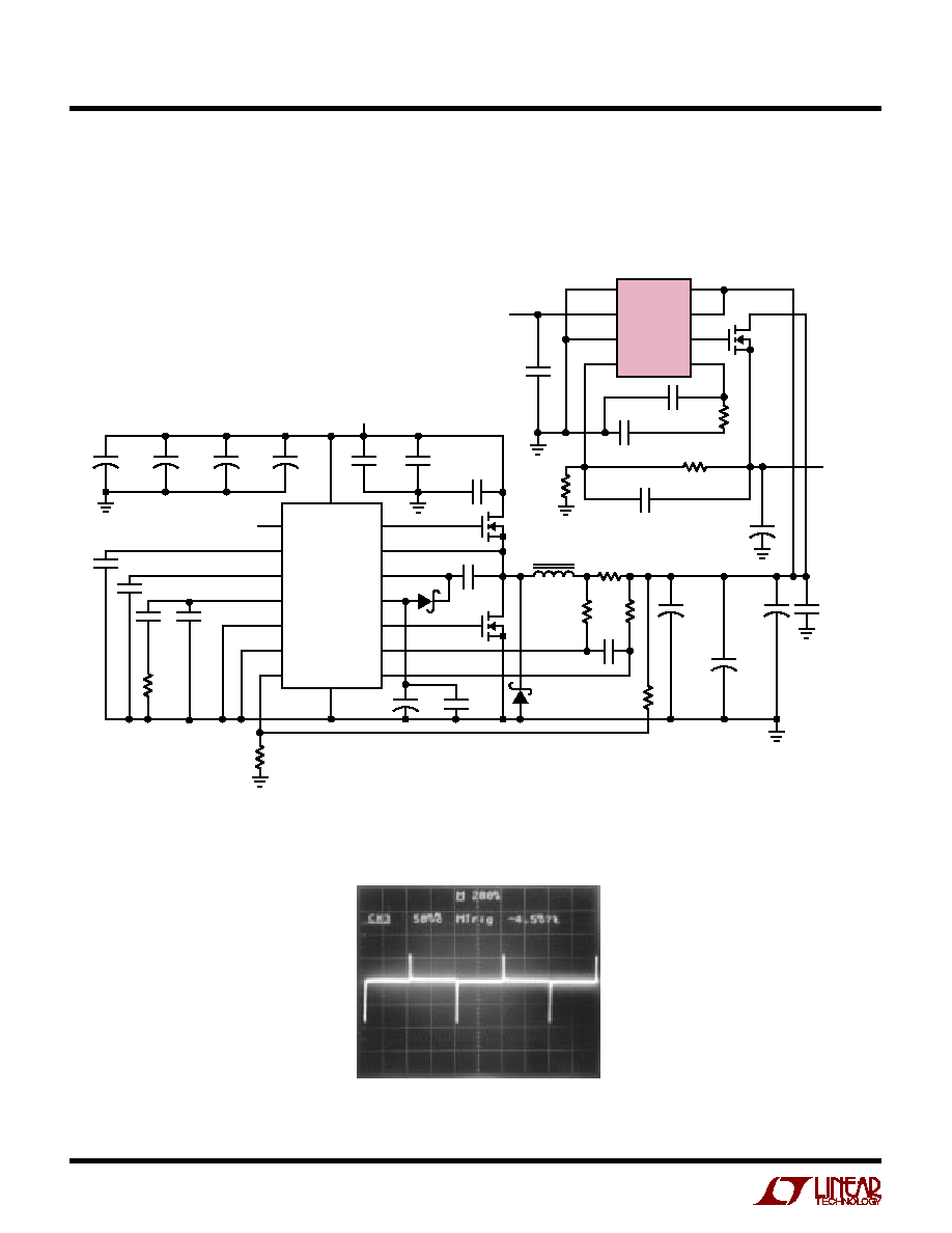
LT1575/LT1577
TYPICAL APPLICATIO
N
S
N
U
12V to 3.3V/9A (14A Peak) Hybrid Regulator
Transient Response to a 10A Load Step
50mV/DIV
200
�
s/DIV
1575/77 TA17
+
+
+
+
+
1575/77 TA16
TG
SW
BOOST
INTV
CC
BG
S
+
S
�
EXTV
CC
C
OSC
RUN/SS
I
TH
SFB
SGND
V
OS
9
1
2
3
4
5
6
16
14
15
12
11
8
7
13
10
C4, 4.7
�
F
C5
0.1
�
F
D2
MBRS330T3
R8
15K
R3
100
R4
100
C18
1000
�
F
10V
C20
1000
�
F
10V
C19
1000
�
F
10V
R6
0.0075
L1
4
�
H
C2, 1000pF
V
IN
LTC1435
C21, 10pF
C22, 1000pF
R2
1.21k
1%
C1, 470pF
R9
2k
Q1
IRLZ44
R1
2.1k, 1%
V
CORE
3.3V
1
2
3
4
8
7
6
5
PGND
D1, CMDSH-3
Q3
Q2
C16
1
�
F
C14
150
�
F
16V
C15
1
�
F
C17
1
�
F
12V
C11
150
�
F
16V
C12
150
�
F
16V
C13
150
�
F
16V
C3, 0.1
�
F
C9
1500pF
R5
16.5k
C10, 1000pF
C8, 68pF
C7, 0.1
�
F
R7
35.7k
+
C23
1
�
F
C6
0.1
�
F
12V
1
�
F
X7R
CERAMIC
0805 CASE
�
40
+
+
L1 =COILTRONICS CTX02-13199
Q2, Q3 =SILICONIX SUD50N03-10
LT1575
SHDN
V
IN
GND
OUT
IPOS
INEG
GATE
COMP

17
LT1575/LT1577
TYPICAL APPLICATIO
N
S
N
U
3.3V to 2.8V
�
100mV at 5.7A with Sense-Less Current Limit and Timer Latchoff
+
+
1
2
3
4
8
7
6
5
C2
330
�
F
6.3V
C3
680pF
C7
10
�
F
C4
1000pF
R1
4.7k
R2
10
C8 TO C31*
1
�
F
Q1
IRL3303
V
CORE
2.8V
C5
22pF
1575/77 TA14
FAULT RESET
C6
0.1
�
F
12V
C1
330
�
F
6.3V
INPUT
3.3V
RTN
+
*X7R CERAMIC 0805 CASE
LT1575-2.8
SHDN
V
IN
GND
OUT
IPOS
INEG
GATE
COMP
N8 1197
0.100
�
0.010
(2.540
�
0.254)
0.065
(1.651)
TYP
0.045 � 0.065
(1.143 � 1.651)
0.130
�
0.005
(3.302
�
0.127)
0.020
(0.508)
MIN
0.018
�
0.003
(0.457
�
0.076)
0.125
(3.175)
MIN
1
2
3
4
8
7
6
5
0.255
�
0.015*
(6.477
�
0.381)
0.400*
(10.160)
MAX
0.009 � 0.015
(0.229 � 0.381)
0.300 � 0.325
(7.620 � 8.255)
0.325
+0.035
�0.015
+0.889
�0.381
8.255
(
)
*THESE DIMENSIONS DO NOT INCLUDE MOLD FLASH OR PROTRUSIONS.
MOLD FLASH OR PROTRUSIONS SHALL NOT EXCEED 0.010 INCH (0.254mm)
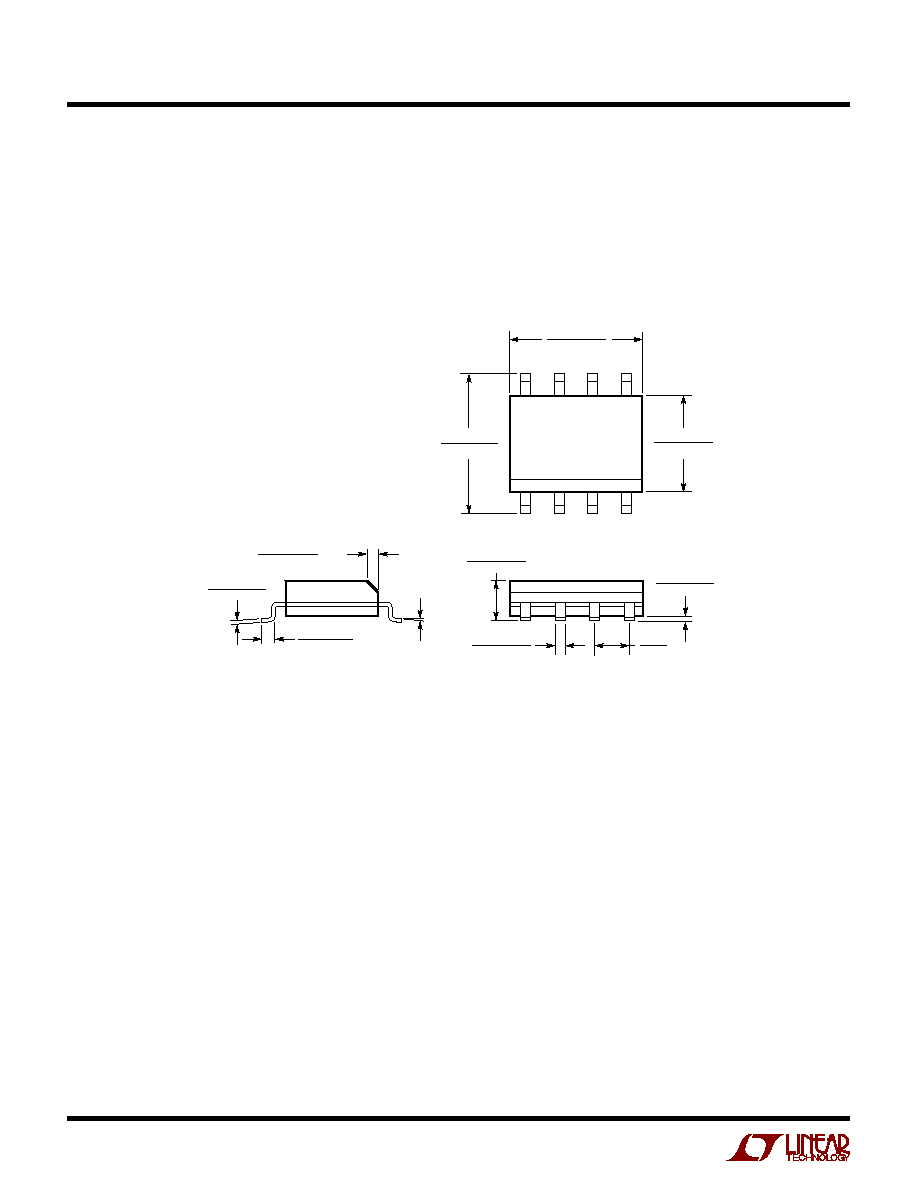
N8 Package
8-Lead PDIP (Narrow 0.300)
(LTC DWG # 05-08-1510)
Dimensions in inches (millimeters) unless otherwise noted.
PACKAGE DESCRIPTIO
N
U
18
LT1575/LT1577
PACKAGE DESCRIPTIO
N
U
Dimensions in inches (millimeters) unless otherwise noted.
S8 Package
8-Lead Plastic Small Outline (Narrow 0.150)
(LTC DWG # 05-08-1610)
1
2
3
4
0.150 � 0.157**
(3.810 � 3.988)
8
7
6
5
0.189 � 0.197*
(4.801 � 5.004)
0.228 � 0.244
(5.791 � 6.197)
0.016 � 0.050
0.406 � 1.270
0.010 � 0.020
(0.254 � 0.508)
�
45
�
0
�
� 8
�
TYP
0.008 � 0.010
(0.203 � 0.254)
SO8 0996
0.053 � 0.069
(1.346 � 1.752)
0.014 � 0.019
(0.355 � 0.483)
0.004 � 0.010
(0.101 � 0.254)
0.050
(1.270)
TYP
DIMENSION DOES NOT INCLUDE MOLD FLASH. MOLD FLASH
SHALL NOT EXCEED 0.006" (0.152mm) PER SIDE
DIMENSION DOES NOT INCLUDE INTERLEAD FLASH. INTERLEAD
FLASH SHALL NOT EXCEED 0.010" (0.254mm) PER SIDE
*
**
19
LT1575/LT1577
PACKAGE DESCRIPTIO
N
U
Dimensions in inches (millimeters) unless otherwise noted.
Information furnished by Linear Technology Corporation is believed to be accurate and reliable.
However, no responsibility is assumed for its use. Linear Technology Corporation makes no represen-
tation that the interconnection of its circuits as described herein will not infringe on existing patent rights.
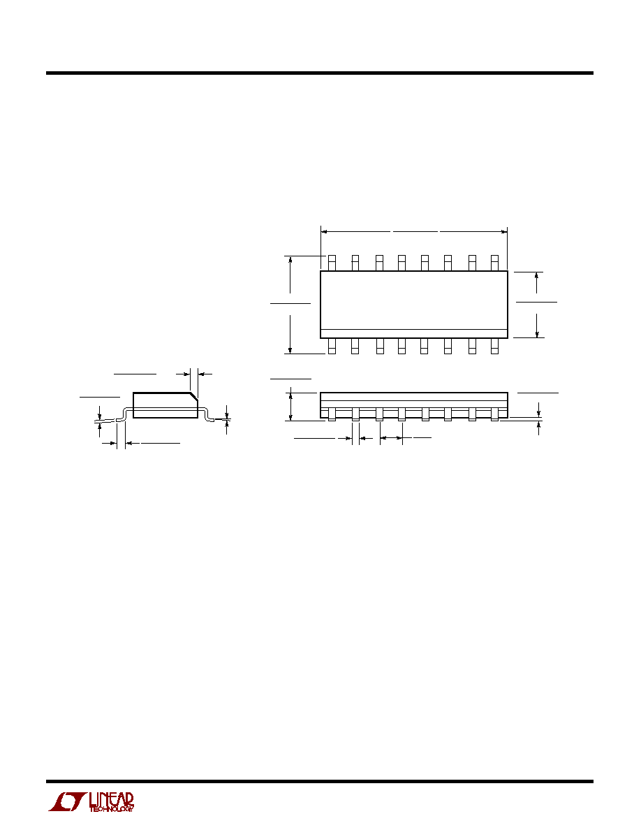
S Package
16-Lead Plastic Small Outline (Narrow 0.150)
(LTC DWG # 05-08-1610)
0.016 � 0.050
0.406 � 1.270
0.010 � 0.020
(0.254 � 0.508)
�
45
�
0
�
� 8
�
TYP
0.008 � 0.010
(0.203 � 0.254)
1
2
3
4
5
6
7
8
0.150 � 0.157**
(3.810 � 3.988)
16
15
14
13
0.386 � 0.394*
(9.804 � 10.008)
0.228 � 0.244
(5.791 � 6.197)
12
11
10
9
S16 0695
0.053 � 0.069
(1.346 � 1.752)
0.014 � 0.019
(0.355 � 0.483)
0.004 � 0.010
(0.101 � 0.254)
0.050
(1.270)
TYP
DIMENSION DOES NOT INCLUDE MOLD FLASH. MOLD FLASH
SHALL NOT EXCEED 0.006" (0.152mm) PER SIDE
DIMENSION DOES NOT INCLUDE INTERLEAD FLASH. INTERLEAD
FLASH SHALL NOT EXCEED 0.010" (0.254mm) PER SIDE
*
**
20
LT1575/LT1577
�
LINEAR TECHNOLOGY CORPORATION 1996
15757f LT/TP 0598 4K � PRINTED IN THE USA
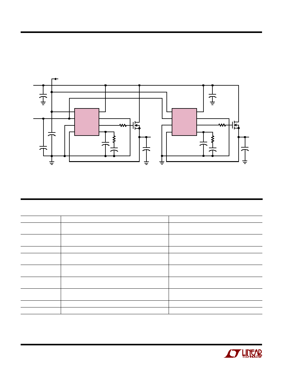
LT1577 Split Plane System
TYPICAL APPLICATIO
N
U
+
C2
330
�
F
6.3V
C3
0.33
�
F
C6
1500pF
R2
3.9k
R1
3.9
R5
3.9
C9 TO
C20*
1
�
F
Q1
IRFZ24
V
I/O
3.3V
C5
10pF
C8
1000pF
R6
7.5k
C7
10pF
1575/77 TA15
FAULT RESET
C4
1
�
F
12V
C1
330
�
F
6.3V
INPUT
5V
+
Q2
IRFZ24
*X7R CERAMIC 0805 CASE
C21 TO
C44*
1
�
F
V
CORE
2.8V
1
2
3
4
16
15
14
13
IPOS1
INEG1
GATE1
COMP1
SHDN1
V
IN1
GND1
OUT-3.3
1/2 LT1577
5
6
7
8
12
11
10
9
IPOS2
INEG2
GATE2
COMP2
SHDN2
V
IN2
GND2
OUT-2.8
1/2 LT1577
Linear Technology Corporation
1630 McCarthy Blvd., Milpitas, CA 95035-7417
(408) 432-1900
q
FAX: (408) 434-0507
q
www.linear-tech.com
RELATED PARTS
PART NUMBER
DESCRIPTION
COMMENTS
LTC1266
Current Mode, Step-Up/Down Switching Regulator Controller
Synchronous N- or P-Channel FETs, Comparator/Low
Battery Detector
LTC1392
Micropower Temperature, Power Supply and Differential
Temperature to Bits Control
Voltage Monitor
LTC1430
High Power Step-Down Switching Regulator Controller
Voltage Mode, 5V to 3.xxV at >10A
LTC1435
High Efficiency, Low Noise Synchronous Step-Down
Current Mode with Wide Input Voltage Range
Switching Regulator
LTC1553
Digitally Controlled Synchronous Switching Regulator Controller
Controller for Pentium II Processor, Buck Conversion
from 5V or 12V Main Power
LTC1553L
Digitally Controlled Synchronous Switching Regulator Controller
Controller for Pentium II Processor, Buck Conversion
from 5V Main Power
LT1573
Low Dropout Regulator Driver
Drives Low Cost PNP Transistor for High Power,
Low Dropout Applications
LT1580
7A, Very Low Dropout Linear Regulator
0.54V Dropout at 7A, Fixed 2.5V
OUT
and Adjustable
LT1585-1.5
Fixed 1.5V, 5A Low Dropout Fast Response Regulator
GTL+ Regulator