 | ÐлекÑÑоннÑй компоненÑ: LT1576I | СкаÑаÑÑ:  PDF PDF  ZIP ZIP |
Äîêóìåíòàöèÿ è îïèñàíèÿ www.docs.chipfind.ru
1
LT1576/LT1576-5
1.5A, 200kHz Step-Down
Switching Regulator
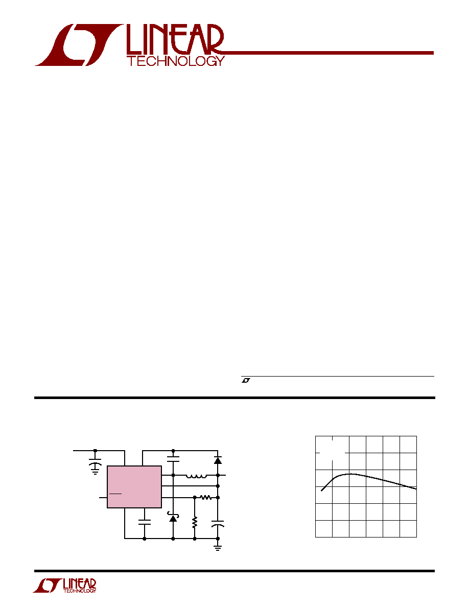
BOOST
LT1576
V
IN
SHDN
OUTPUT**
5V, 1.25A
* RIPPLE CURRENT RATING
I
OUT
/2
** INCREASE L1 TO 30
µ
H FOR LOAD
CURRENTS ABOVE 0.6A AND TO
60
µ
H ABOVE 1A
SEE APPLICATIONS INFORMATION
INPUT
6V TO 25V
1576 TA01
C2
0.33
µ
F
C
C
100pF
D1
1N5818
C1
100
µ
F, 10V
SOLID
TANTALUM
C3*
10
µ
F TO
50
µ
F
OPEN = ON
D2
1N914
L1**
15
µ
H
V
SW
FB
BIAS
GND
V
C
+
+
R2
4.99k
R1
15.8k
5V Buck Converter
Efficiency vs Load Current
s
Constant 200kHz Switching Frequency
s
1.21V Reference Voltage
s
Fixed 5V Output Option
s
Easily Synchronizable
s
Uses All Surface Mount Components
s
Inductor Size Reduced to 15
µ
H
s
Saturating Switch Design: 0.2
s
Effective Supply Current: 1.16mA
s
Shutdown Current: 20
µ
A
s
Cycle-by-Cycle Current Limiting
s
Fused Lead SO-8 Package
The LT
®
1576 is a 200kHz monolithic buck mode switching
regulator. A 1.5A switch is included on the die along with
all the necessary oscillator, control and logic circuitry. The
topology is current mode for fast transient response and
good loop stability. The LT1576 is a modified version of the
industry standard LT1376 optimized for noise sensitive
applications.
In addition, the reference voltage has been lowered to
allow the device to produce output voltages down to 1.2V.
Quiescent current has been reduced by a factor of two.
Switch on resistance has been reduced by 30%. Switch tran-
sition times have been slowed to reduce EMI generation.
The oscillator frequency has been reduced to 200kHz to
maintain high efficiency over a wide output current range.
The pinout has been changed to improve PC layout by
allowing the high current high frequency switching cir-
cuitry to be easily isolated from low current noise sensitive
control circuitry. The new SO-8 package includes a fused
ground lead which significantly reduces the thermal resis-
tance of the device to extend the ambient operating tem-
perature range. There is an optional function of shutdown
or synchronization. Standard surface mount external parts
can be used including the inductor and capacitors.
s
Portable Computers
s
Battery-Powered Systems
s
Battery Charger
s
Distributed Power
, LTC and LT are registered trademarks of Linear Technology Corporation.
LOAD CURRENT (A)
0
EFFICIENCY (%)
100
95
90
85
80
75
70
0.25
0.50
0.75
1.00
1576 TA02
1.25
1.50
V
OUT
= 5V
V
IN
= 10V
L = 33
µ
H
FEATURES
DESCRIPTIO
U
APPLICATIO S
U
TYPICAL APPLICATIO
N
U
2
LT1576/LT1576-5
ABSOLUTE
M
AXI
M
U
M
RATINGS
W
W
W
U
PACKAGE/ORDER I
N
FOR
M
ATIO
N
W
U
U
(Note 1)
Input Voltage .......................................................... 25V
BOOST Pin Above Input Voltage ............................. 10V
SHDN Pin Voltage ..................................................... 7V
BIAS Pin Voltage ...................................................... 7V
FB Pin Voltage (Adjustable Part) ............................ 3.5V
FB Pin Current (Adjustable Part) ............................ 1mA
SYNC Pin Voltage ..................................................... 7V
Operating Junction Temperature Range
LT1576C ............................................... 0
°
C to 125
°
C
LT1576I ........................................... 40
°
C to 125
°
C
Storage Temperature Range ................ 65
°
C to 150
°
C
Lead Temperature (Soldering, 10 sec)................. 300
°
C
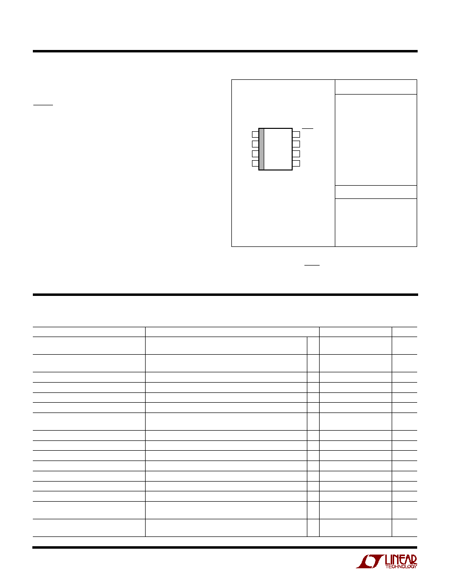
ORDER PART NUMBER
LT1576CS8
LT1576CS8-SYNC
LT1576IS8
LT1576IS8-SYNC
LT1576CS8-5
LT1576CS8-5 SYNC
LT1576IS8-5
LT1576IS8-5 SYNC
S8 PART MARKING
1576
1576SN
1576I
576ISN
*Default is the adjustable output voltage device with FB pin and shutdown
function. Option -5 replaces FB with SENSE pin for fixed 5V output
applications. -SYNC replaces SHDN with SYNC pin for applications
requiring synchronization. Consult factory for Military grade parts.
1
2
3
4
8
7
6
5
TOP VIEW
S8 PACKAGE
8-LEAD PLASTIC SO
V
SW
V
IN
BOOST
GND
FB OR SENSE*
V
C
BIAS
SHDN OR
SYNC*
JA
= 80
°
C/ W WITH FUSED GROUND PIN
CONNECTED TO GROUND PLANE OR
LARGE LANDS
PARAMETER
CONDITIONS
MIN
TYP
MAX
UNITS
Feedback Voltage
1.195
1.21
1.225
V
All Conditions
q
1.18
1.24
V
Sense Voltage (Fixed 5V)
4.94
5.0
5.06
V
All Conditions
q
4.90
5.10
V
SENSE Pin Resistance
13
18.5
26
k
Reference Voltage Line Regulation
5V
V
IN
25V
0.01
0.03
%/V
Feedback Input Bias Current
q
0.5
2
µ
A
Error Amplifier Voltage Gain
(Notes 2, 8)
200
400
Error Amplifier Transconductance
I (V
C
) =
±
10
µ
A (Note 8)
800
1050
1300
µ
Mho
q
400
1700
µ
Mho
V
C
Pin to Switch Current Transconductance
1.5
A/ V
Error Amplifier Source Current
V
FB
= 1.1V
q
40
110
190
µ
A
Error Amplifier Sink Current
V
FB
= 1.4V
q
50
130
200
µ
A
V
C
Pin Switching Threshold
Duty Cycle = 0
0.8
V
V
C
Pin High Clamp
2.1
V
Switch Current Limit
V
C
Open, V
FB
= 1.1V, DC
50%
q
1.5
2
3.50
A
Slope Compensation (Note 9)
DC = 80%
0.3
A
Switch On Resistance (Note 7)
I
SW
= 1.5A
0.2
0.35
q
0.45
Maximum Switch Duty Cycle
V
FB
= 1.1V
90
94
%
q
86
94
%
ELECTRICAL CHARACTERISTICS
The
q
denotes specifications which apply over the full operating temperature
range, otherwise specifications are T
A
, T
J
= 25
°
C, V
IN
= 15V, V
C
= 1.5V, Boost = V
IN
+ 5V, switch open, unless otherwise noted.
15765
5765SN
1576I5
76I5SN
3
LT1576/LT1576-5
PARAMETER
CONDITIONS
MIN
TYP
MAX
UNITS
Minimum Switch Duty Cycle (Note 10)
8
%
Switch Frequency
V
C
Set to Give 50% Duty Cycle
180
200
220
kHz
q
160
240
kHz
Switch Frequency Line Regulation
5V
V
IN
25V
q
0
0.15
%/ V
Frequency Shifting Threshold on FB Pin
f = 10kHz
q
0.4
0.74
1.0
V
Minimum Input Voltage (Note 3)
q
5.0
5.5
V
Minimum Boost Voltage (Note 4)
I
SW
1.5A
q
2.3
3.0
V
Boost Current (Note 5)
I
SW
= 0.5A
q
9
18
mA
I
SW
= 1.5A
q
27
50
mA
V
IN
Supply Current (Note 6)
V
BIAS
= 5V
q
0.55
0.8
mA
BIAS Supply Current (Note 6)
V
BIAS
= 5V
q
1.6
2.2
mA
Shutdown Supply Current
V
SHDN
= 0V, V
IN
25V, V
SW
= 0V, V
C
Open
20
50
µ
A
q
75
µ
A
Lockout Threshold
V
C
Open
q
2.34
2.42
2.50
V
Shutdown Thresholds
V
C
Open Device Shutting Down
q
0.13
0.37
0.60
V
Device Starting Up
q
0.25
0.45
0.7
V
Synchronization Threshold
1.5
2.2
V
Synchronizing Range
250
400
kHz
SYNC Pin Input Resistance
40
k
Note 1: Absolute Maximum Ratings are those values beyond which the life
of a device may be impaired.
Note 2: Gain is measured with a V
C
swing equal to 200mV above the
switching threshold level to 200mV below the upper clamp level.
Note 3: Minimum input voltage is not measured directly, but is guaranteed
by other tests. It is defined as the voltage where internal bias lines are still
regulated so that the reference voltage and oscillator frequency remain
constant. Actual minimum input voltage to maintain a regulated output will
depend on output voltage and load current. See Applications Information.
Note 4: This is the minimum voltage across the boost capacitor needed to
guarantee full saturation of the internal power switch.
Note 5: Boost current is the current flowing into the boost pin with the pin
held 5V above input voltage. It flows only during switch on time.
Note 6: V
IN
supply current is the current drawn when the BIAS pin is held
at 5V and switching is disabled. Total input referred supply current is
calculated by summing input supply current (I
SI
) with a fraction of BIAS
supply current (I
SB
)
I
TOT
= I
SI
+ (I
SB
)(V
BIAS
/V
IN
)(1.15)
with V
IN
= 15V, V
BIAS
= 5V, I
SI
= 0.55mA, I
SB
= 1.6mA and I
TOT
= 1.16mA.
If the BIAS pin is unavailable or open circuit, the sum of V
IN
and BIAS
supply currents will be drawn by the V
IN
pin.
Note 7: Switch on resistance is calculated by dividing V
IN
to V
SW
voltage
by the forced current (1.5A). See Typical Performance Characteristics for
the graph of switch voltage at other currents.
Note 8: Transconductance and voltage gain refer to the internal amplifier
exclusive of the voltage divider. To calculate gain and transconductance,
refer to the SENSE pin on the fixed voltage parts. Divide values shown by
the ratio V
OUT
/1.21.
Note 9: Slope compensation is the current subtracted from the switch
current limit at 80% duty cycle. See Maximum Output Load Current in the
Applications Information section for further details.
Note 10: Minimum on-time is 400ns typical. For a 200kHz operating
frequency this means the minimum duty cycle is 8%. In frequency
foldback mode, the effective duty cycle will be less than 8%.
ELECTRICAL CHARACTERISTICS
The
q
denotes specifications which apply over the full operating temperature
range, otherwise specifications are T
A
, T
J
= 25
°
C, V
IN
= 15V, V
C
= 1.5V, Boost = V
IN
+ 5V, switch open, unless otherwise noted.
4
LT1576/LT1576-5
TYPICAL PERFOR
M
A
N
CE CHARACTERISTICS
U
W
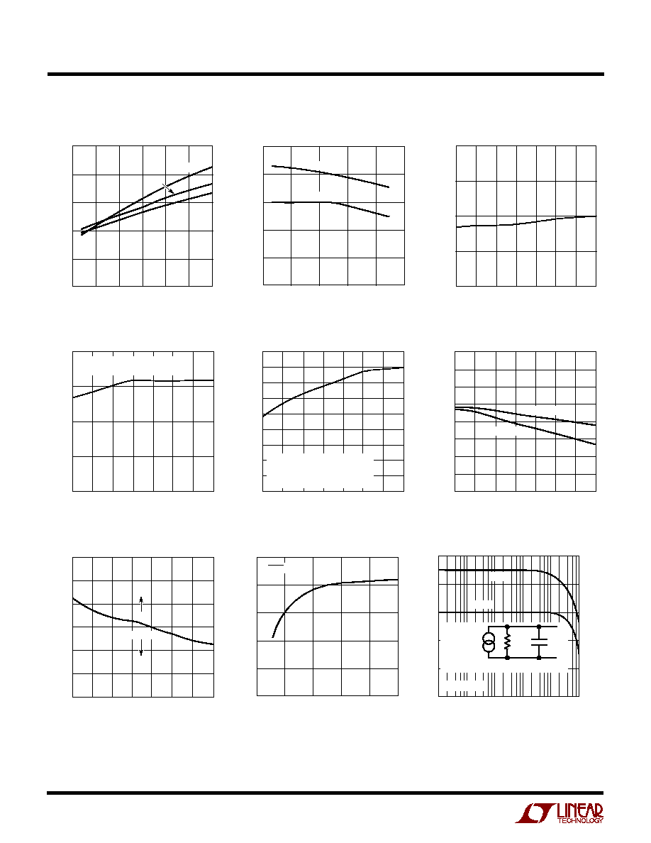
JUNCTION TEMPERATURE (
°
C)
50
4
3
2
1
0
100
1576 G04
25
0
25
50
75
125
CURRENT (
µ
A)
AT 2.44V STANDBY THRESHOLD
(CURRENT FLOWS OUT OF PIN)
Shutdown Pin Bias Current
JUNCTION TEMPERATURE (
°
C)
50
180
160
140
120
100
80
60
40
20
0
100
1576 G05
25
0
25
50
75
125
CURRENT (
µ
A)
CURRENT REQUIRED TO FORCE
SHUTDOWN (FLOWS OUT OF PIN).
AFTER SHUTDOWN, CURRENT
DROPS TO A FEW
µ
A
Shutdown Pin Bias Current
JUNCTION TEMPERATURE (
°
C)
50
SHUTDOWN PIN VOLTAGE (V)
100
1576 G06
0
50
0.8
0.7
0.6
0.5
0.4
0.3
0.2
0.1
0
25
25
75
125
START-UP
SHUTDOWN
Shutdown Supply Current
INPUT VOLTAGE (V)
0
INPUT SUPPLY CURRENT (
µ
A)
25
20
15
10
5
0
20
1576 G08
5
10
15
25
V
SHDN
= 0V
FREQUENCY (Hz)
GAIN (
µ
Mho)
PHASE (DEG)
2000
1500
1000
500
0
500
200
150
100
50
0
50
10
1k
10k
1M
1576 G09
100
100k
GAIN
PHASE
ERROR AMPLIFIER EQUIVALENT CIRCUIT
R
OUT
570k
C
OUT
2.4pF
V
C
R
LOAD
= 50
V
FB
1
×
10
3
)
(
Error Amplifier Transconductance
JUNCTION TEMPERATURE (
°
C)
50
SHUTDOWN PIN VOLTAGE (V)
2.46
2.45
2.44
2.43
2.42
2.41
2.40
25
75
1576 G07
25
0
50
100
125
ON
STANDBY
Shutdown Thresholds
Standby Thresholds
Switch Drop
JUNCTION TEMPERATURE (
°
C)
50
1.23
1.22
1.21
1.20
1.19
100
1576 G03
25
0
25
50
75
125
FEEDBACK VOLTAGE (V)
SWITCH CURRENT (A)
0
SWITCH VOLTAGE (V)
0.5
0.4
0.3
0.2
0.1
0
0.25
0.50
0.75
1.00
1576 G01
1.25
1.50
125
°
C
20
°
C
25
°
C
Feedback Pin Voltage
Switch Peak Current Limit
DUTY CYCLE (%)
0
SWITCH PEAK CURRENT (A)
2.5
2.0
1.5
1.0
0.5
0
80
1576 G02
20
40
60
100
TYPICAL
MINIMUM
5
LT1576/LT1576-5
TYPICAL PERFOR
M
A
N
CE CHARACTERISTICS
U
W
Kool M
µ
is a registered trademark of Magnetics, Inc.
JUNCTION TEMPERATURE (
°
C)
50
240
220
200
180
160
100
1576 G13
25
0
25
50
75
125
FREQUENCY (kHz)
Switching Frequency
INPUT VOLTAGE (V)
0
CURRENT (A)
1.50
1.25
1.00
0.75
0.50
0.25
0
5
10
15
20
1576 G15
25
V
OUT
= 10V
L = 60
µ
H
L = 30
µ
H
L = 15
µ
H
Maximum Load Current
at V
OUT
= 10V
LOAD CURRENT (mA)
1
INPUT VOLTAGE (V)
7
6
5
10
V
OUT
= 5V
100
1000
1576 G14
MINIMUM
STARTING VOLTAGE
MINIMUM
RUNNING VOLTAGE
Minimum Input Voltage
at V
OUT
= 5V
INPUT VOLTAGE (V)
0
CURRENT (A)
1.50
1.25
1.00
0.75
0.50
0.25
0
5
10
15
20
1576 G16
25
V
OUT
= 5V
L = 60
µ
H
L = 30
µ
H
L = 15
µ
H
Maximum Load Current
at V
OUT
= 5V
INDUCTANCE (
µ
H)
0
5
CORE LOSS (W)
CORE LOSS (% OF 5W LOAD)
1.0
0.1
0.01
0.001
10
15
20
20
12
8
4
2
1.2
0.8
0.4
0.2
0.12
0.08
0.04
0.02
25
1576 G18
TYPE 52
POWDERED IRON
Kool M
µ
®
PERMALLOY
µ
= 125
V
OUT
= 5V, V
IN
= 10V, I
OUT
= 1A
CORE LOSS IS
INDEPENDENT OF LOAD
CURRENT UNTIL LOAD CURRENT FALLS
LOW ENOUGH FOR CIRCUIT TO GO INTO
DISCONTINUOUS MODE
Inductor Core Loss
INPUT VOLTAGE (V)
0
CURRENT (A)
1.50
1.25
1.00
0.75
0.50
0.25
0
5
10
15
20
1576 G17
25
V
OUT
= 3.3V
L = 30
µ
H
L = 15
µ
H
L = 60
µ
H
Maximum Load Current
at V
OUT
= 3.3V
FEEDBACK VOLTAGE (V)
0
SWITCHING FREQUENCY (kHz)
OR CURRENT (
µ
A)
2.0
1576 G12
0.5
1.0
1.5
250
200
150
100
50
0
FEEDBACK PIN CURRENT
SWITCHING FREQUENCY
Shutdown Supply Current
JUNCTION TEMPERATURE (
°
C)
50
TRANSCONDUCTANCE (
µ
Mho)
100
1576 G11
0
50
1600
1400
1200
1000
800
600
400
200
0
25
25
75
125
Error Amplifier Transconductance
Frequency Foldback
SHUTDOWN VOLTAGE (V)
0
INPUT SUPPLY CURRENT (
µ
A)
0.4
1576 G10
0.1
0.2
0.3
100
75
50
25
0
V
IN
= 25V
V
IN
= 10V