/home/web/doc/html/liner/177582
1
LT1579
300mA Dual Input Smart
Battery Backup Regulator
Daisy-Chained Control Outputs
FEATURES
The LT
®
1579 is a dual input, single output, low dropout
regulator. This device is designed to provide an
uninterruptible output voltage from two independent input
voltage sources on a priority basis. All of the circuitry
needed to switch smoothly and automatically between
inputs is incorporated.
The LT1579 can supply 300mA of output current from
either input at a dropout voltage of 0.4V. Quiescent current
is 50
µ
A, dropping to 7
µ
A in shutdown. Two comparators
are included to monitor input voltage status. Two addi-
tional status flags indicate which input is supplying power
and provide an early warning against loss of output
regulation when both inputs are low. A secondary select
pin is provided so that the user can force the device to
switch from the primary input to the secondary input.
Internal protection circuitry includes reverse-battery pro-
tection, current limiting, thermal limiting and reverse-
current protection.
The device is available in fixed output voltages of 3V, 3.3V
and 5V, and as an adjustable device with a 1.5V reference
voltage. The LT1579 regulators are available in narrow
16-lead SO and 16-lead SSOP packages with all features,
and in SO-8 with limited features.
DESCRIPTIO
N
U
s
Maintains Output Regulation with Dual Inputs
s
Dropout Voltage: 0.4V
s
Output Current: 300mA
s
50
µ
A Quiescent Current
s
No Protection Diodes Needed
s
Two Low-Battery Comparators
s
Status Flags Aid Power Management
s
Adjustable Output from 1.5V to 20V
s
Fixed Output Voltages: 3V, 3.3V and 5V
s
7
µ
A Quiescent Current in Shutdown
s
Reverse-Battery Protection
s
Reverse Current Protection
s
Remove, Recharge and Replace Batteries Without
Loss of Regulation
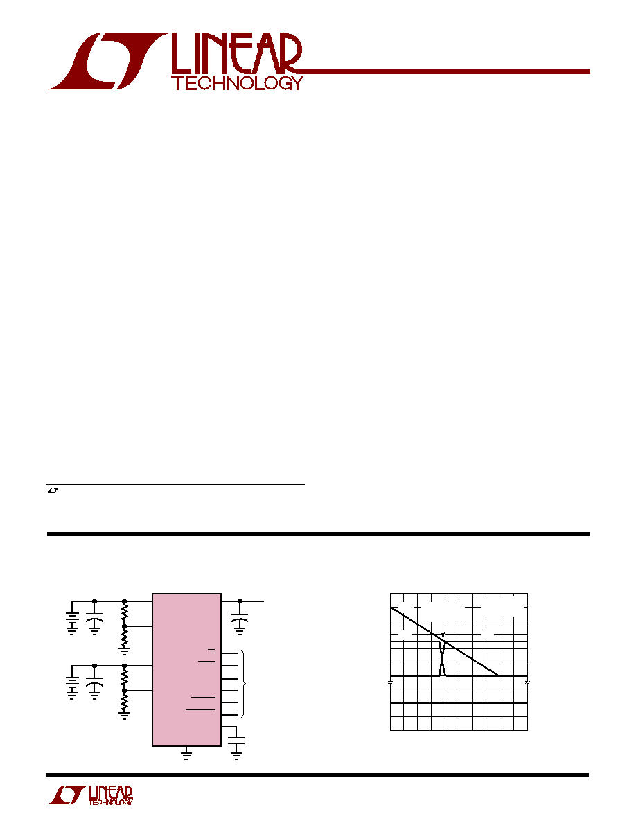
5V Dual Battery Supply
Automatic Input Switching
2.7M
1M
2.7M
1M
+
1
µ
F
+
1
µ
F
+
4.7
µ
F
5V
300mA
TO
POWER
MANAGEMENT
0.01
µ
F
IN1
OUT
SS
SHDN
LBO1
LB02
BACKUP
DROPOUT
BIASCOMP
LBI1
IN2
LBI2
GND
LT1579-5
1579 TA01
TIME (ms)
0
INPUT VOLTAGE (V)
OUTPUT VOLTAGE (V)
4
8
12
16
1578 TA02
0
5.00
2
6
INPUT CURRENT (mA)
40
80
0
20
60
10
5.05
4.95
4
8
12
2
18
6
10
14
20
V
IN2
= 10V
I
LOAD
= 50mA
SWITCHOVER
POINT
V
IN1
I
IN1
I
IN2
APPLICATIO
N
S
U
s
Dual Battery Systems
s
Battery Backup Systems
s
Automatic Power Management for
Battery-Operated Systems
TYPICAL APPLICATIO
N
U
, LTC and LT are registered trademarks of Linear Technology Corporation.
2
LT1579
T
JMAX
= 125
°
C,
JA
= 90
°
C/W
ABSOLUTE
M
AXI
M
U
M
RATINGS
W
W
W
U
Power Input Pin Voltage ......................................
±
20V*
Output Pin Voltage
Fixed Devices............................................. 6.5V, 6V
Adjustable Device ............................................
±
20V*
Output Pin Reverse Current .................................... 5mA
ADJ Pin Voltage .............................................. 2V, 0.6V
ADJ Pin Current ...................................................... 5mA
Control Input Pin Voltage ............................ 6.5V, 0.6V
Control Input Pin Current ....................................... 5mA
W
U
U
PACKAGE/ORDER I FOR ATIO
BIASCOMP Pin Voltage ............................... 6.5V, 0.6V
BIASCOMP Pin Current .......................................... 5mA
Logic Flag Output Voltage ............................ 6.5V, 0.6V
Logic Flag Input Current ......................................... 5mA
Output Short-Circuit Duration .......................... Indefinite
Storage Temperature Range ................. 65
°
C to 150
°
C
Operating Junction Temperature Range .... 0
°
C to 125
°
C
Lead Temperature (Soldering, 10 sec) .................. 300
°
C
*For applications requiring input voltage ratings greater than 20V,
consult factory.
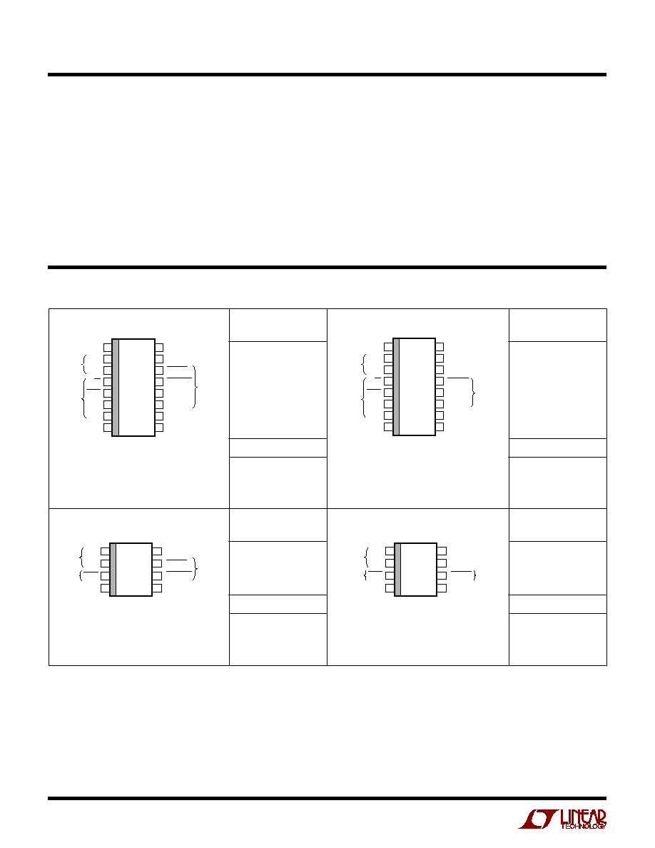
ORDER PART
NUMBER
ORDER PART
NUMBER
Consult factory for Industrial and Military grade parts.
SEE APPLICATION INFORMATION SECTION
T
JMAX
= 125
°
C,
JA
= 90
°
C/W
SEE APPLICATION INFORMATION SECTION
LT1579CS8
S8 PART MARKING
15793
157933
15795
LT1579CS8-3
LT1579CS8-3.3
LT1579CS8-5
ORDER PART
NUMBER
S8 PART MARKING
1579
ORDER PART
NUMBER
SEE APPLICATION INFORMATION SECTION
TOP VIEW
1
2
3
4
5
6
7
8
16
15
14
13
12
11
10
9
GND
VIN1
VIN2
SS
SHDN
LBI1
LBI2
GND
GND
OUT
BACKUP
DROPOUT
LBO1
LBO2
BIASCOMP
GND
POWER
INPUTS
CONTROL
INPUTS
LOGIC
OUTPUTS
GN PACKAGE
16-LEAD PLASTIC SSOP
S PACKAGE
16-LEAD PLASTIC SO
T
JMAX
= 125
°
C,
JA
= 95
°
C/W (GN)
T
JMAX
= 125
°
C,
JA
= 68
°
C/W (S)
T
JMAX
= 125
°
C,
JA
= 95
°
C/W (GN)
T
JMAX
= 125
°
C,
JA
= 68
°
C/W (S)
SEE APPLICATION INFORMATION SECTION
TOP VIEW
GN PACKAGE
16-LEAD PLASTIC SSOP
S PACKAGE
16-LEAD PLASTIC SO
1
2
3
4
5
6
7
8
16
15
14
13
12
11
10
9
GND
VIN1
VIN2
SS
SHDN
LBI1
LBI2
GND
GND
OUT
ADJ
BACKUP
LBO1
LBO2
BIASCOMP
GND
POWER
INPUTS
CONTROL
INPUTS
LOGIC
OUTPUTS
1
2
3
4
8
7
6
5
TOP VIEW
OUT
BACKUP
DROPOUT
BIASCOMP
V
IN1
V
IN2
SHDN
GND
S8 PACKAGE
8-LEAD PLASTIC SO
POWER
INPUTS
CONTROL
INPUT
LOGIC
OUTPUTS
1
2
3
4
8
7
6
5
TOP VIEW
OUT
ADJ
BACKUP
BIASCOMP
V
IN1
V
IN2
SHDN
GND
S8 PACKAGE
8-LEAD PLASTIC SO
POWER
INPUTS
CONTROL
INPUT
LOGIC
OUTPUT
LT1579CGN-3
LT1579CGN-3.3
LT1579CGN-5
LT1579CS-3
LT1579CS-3.3
LT1579CS-5
LT1579CGN
LT1579CS
GN PART MARKING
15793
157933
15795
GN PART MARKING
1579
3
LT1579
ELECTRICAL CHARACTERISTICS
PARAMETER
CONDITIONS
MIN
TYP
MAX
UNITS
Regulated Output
LT1579-3
V
IN1
= V
IN2
= 3.5V, I
LOAD
= 1mA, T
J
= 25
°
C
2.950
3.000
3.050
V
Voltage (Note 1)
4V < V
IN1
< 20V, 4V < V
IN2
< 20V, 1mA < I
LOAD
< 300mA
q
2.900
3.000
3.100
V
LT1579-3.3 V
IN1
= V
IN2
= 3.8V, I
LOAD
= 1mA, T
J
= 25
°
C
3.250
3.300
3.350
V
4.3V < V
IN1
< 20V, 4.3V < V
IN2
< 20V, 1mA < I
LOAD
< 300mA
q
3.200
3.300
3.400
V
LT1579-5
V
IN1
= V
IN2
= 5.5V, I
LOAD
= 1mA, T
J
= 25
°
C
4.925
5.000
5.075
V
6V < V
IN1
< 20V, 6V < V
IN2
< 20V, 1mA < I
LOAD
< 300mA
q
4.850
5.000
5.150
V
Adjust Pin Voltage
LT1579
V
IN1
= V
IN2
= 3.2V, I
LOAD
= 1mA, T
J
= 25
°
C (Note 2)
1.475
1.500
1.525
V
3.7V < V
IN1
< 20V, 3.7V < V
IN2
< 20V, 1mA < I
LOAD
< 300mA
q
1.450
1.500
1.550
V
Line Regulation
LT1579-3
V
IN1
= 3.5V to 20V,
V
IN2
= 3.5V to 20V, I
LOAD
= 1mA
q
1.5
10
mV
LT1579-3.3
V
IN1
= 3.8V to 20V,
V
IN2
= 3.8V to 20V, I
LOAD
= 1mA
q
1.5
10
mV
LT1579-5
V
IN1
= 5.5V to 20V,
V
IN2
= 5.5V to 20V, I
LOAD
= 1mA
q
1.5
10
mV
LT1579
V
IN1
= 3.2V to 20V,
V
IN2
= 3.2V to 20V, I
LOAD
= 1mA (Note 2)
q
1.5
10
mV
Load Regulation
LT1579-3
V
IN1
= V
IN2
= 4V,
I
LOAD
= 1mA to 300mA, T
J
= 25
°
C
3
12
mV
V
IN1
= V
IN2
= 4V,
I
LOAD
= 1mA to 300mA
q
25
mV
LT1579-3.3 V
IN1
= V
IN2
= 4.3V,
I
LOAD
= 1mA to 300mA, T
J
= 25
°
C
3
12
mV
V
IN1
= V
IN2
= 4.3V,
I
LOAD
= 1mA to 300mA
q
25
mV
LT1579-5
V
IN1
= V
IN2
= 6V,
I
LOAD
= 1mA to 300mA, T
J
= 25
°
C
5
15
mV
V
IN1
= V
IN2
= 6V,
I
LOAD
= 1mA to 300mA
q
35
mV
LT1579
V
IN1
= V
IN2
= 3.7V,
I
LOAD
= 1mA to 300mA, T
J
= 25
°
C (Note 2)
2
10
mV
V
IN1
= V
IN2
= 3.7V,
I
LOAD
= 1mA to 300mA
q
20
mV
Dropout Voltage
I
LOAD
= 10mA, T
J
= 25
°
C
0.10
0.28
V
(Notes 3, 4)
I
LOAD
= 10mA
q
0.39
V
V
IN1
= V
IN2
=
I
LOAD
= 50mA, T
J
= 25
°
C
0.18
0.35
V
V
OUT(NOMINAL)
I
LOAD
= 50mA
q
0.45
V
I
LOAD
= 150mA, T
J
= 25
°
C
0.25
0.47
V
I
LOAD
= 150mA
q
0.60
V
I
LOAD
= 300mA, T
J
= 25
°
C
0.34
0.60
V
I
LOAD
= 300mA
q
0.75
V
Ground Pin Current
I
LOAD
= 0mA, T
J
= 25
°
C
50
100
µ
A
(Note 5)
I
LOAD
= 0mA
q
400
µ
A
V
IN1
= V
IN2
=
I
LOAD
= 1mA, T
J
= 25
°
C
100
200
µ
A
V
OUT(NOMINAL)
+ 1V
I
LOAD
= 1mA
q
500
µ
A
I
LOAD
= 50mA
q
0.7
1.5
mA
I
LOAD
= 150mA
q
2
4
mA
I
LOAD
= 300mA
q
5.8
12
mA
Standby Current
I
VIN2
: V
IN1
= 20V, V
IN2
= V
OUT(NOMINAL)
+ 0.5V, V
SS
= Open (HI)
q
3.3
7.0
µ
A
(Note 6) I
LOAD
= 0mA
I
VIN1
: V
IN1
= V
OUT(NOMINAL)
+ 0.5V, V
IN2
= 20V, V
SS
= 0V
q
2.0
7.0
µ
A
Shutdown Threshold
V
OUT
= Off to On
q
0.9
2.8
V
V
OUT
= On to Off
q
0.25
0.75
V
Shutdown Pin Current
V
SHDN
= 0V
q
1.3
5
µ
A
(Note 7)
Quiescent Current in
I
VIN1
: V
IN1
= 20V, V
IN2
= 6V, V
SHDN
= 0V
q
5
12
µ
A
Shutdown (Note 9)
I
VIN2
: V
IN1
= 6V, V
IN2
= 20V, V
SHDN
= 0V
q
5
12
µ
A
I
SRC
: V
IN1
= V
IN2
= 20V, V
SHDN
= 0V
3
µ
A
4
LT1579
ELECTRICAL CHARACTERISTICS
PARAMETER
CONDITIONS
MIN
TYP
MAX
UNITS
Adjust Pin Bias Current
T
J
= 25
°
C
6
30
nA
(Notes 2, 7)
Minimum Input Voltage
I
LOAD
= 0mA
q
2.7
3.2
V
(Note 8)
Minimum Load Current
LT1579
V
IN1
= V
IN2
= 3.2V
q
3
µ
A
Secondary Select
Switch from V
IN2
to V
IN1
q
1.2
2.8
V
Threshold
Switch from
V
IN1
to V
IN2
q
0.25
0.75
V
Secondary Select Pin
V
SS
= 0V
q
1
1.5
µ
A
Current (Note 7)
Low-Battery Trip Threshold
V
IN1
= V
IN2
= V
OUT(NOMINAL)
+ 1V, High-to-Low Transition
q
1.440
1.500
1.550
V
Low-Battery Comparator
V
IN1
= V
IN2
= 6V, I
LBO
= 20
µ
A (Note 11)
q
18
30
mV
Hysteresis
Low-Battery Comparator
V
IN1
= V
IN2
= 6V, V
LBI
= 1.4V, T
J
= 25
°
C
2
5
nA
Bias Current (Notes 7, 10)
Logic Flag Output Voltage
I
SINK
= 20
µ
A
q
0.17
0.45
V
I
SINK
= 5mA
q
0.97
1.3
V
Ripple Rejection
V
IN1
V
OUT
= V
IN2
V
OUT
= 1.2V (Avg), V
RIPPLE
= 0.5V
P-P
55
70
dB
f
RIPPLE
= 120Hz, I
LOAD
= 150mA
Current Limit
V
IN1
= V
IN2
= V
OUT(NOMINAL)
+ 1V,
V
OUT
= 0.1V
q
320
400
mA
Input Reverse Leakage
V
IN1
= V
IN2
= 20V, V
OUT
= 0V
q
1.0
mA
Current
Reverse Output Current
LT1579-3
V
OUT
= 3V, V
IN1
= V
IN2
= 0V
3
12
µ
A
LT1579-3.3 V
OUT
= 3.3V, V
IN1
= V
IN2
= 0V
3
12
µ
A
LT1579-5
V
OUT
= 5V, V
IN1
= V
IN2
= 0V
3
12
µ
A
The
q
denotes specifications which apply over the full operating
temperature range.
Note 1: Operating conditions are limited by maximum junction
temperature. The regulated output voltage specification will not apply for
all possible combinations of input voltage and output current. When
operating at maximum input voltage, output current must be limited.
When operating at maximum output current, the input voltage range must
be limited.
Note 2: The LT1579 (adjustable version) is tested and specified with the
adjust pin connected to the output pin and a 3
µ
A DC load.
Note 3: Dropout voltage is the minimum input-to-output voltage
differential required to maintain regulation at the specified output current.
In dropout, the output voltage will be equal to V
IN
V
DROPOUT
.
Note 4: To meet the requirements for minimum input voltage, the LT1579
(adjustable version) is connected with an external resistor divider for a
3.3V output voltage (see curve of Minimum Input Voltage vs Temperature
in the Typical Performance Characteristics). For this configuration,
V
OUT(NOMINAL)
= 3.3V.
Note 5: Ground pin current will rise at T
J
> 75
°
C. This is due to internal
circuitry designed to compensate for leakage currents in the output
transistor at high temperatures. This allows quiescent current to be
minimized at lower temperatures, yet maintain output regulation at high
temperatures with light loads. See the curve of Quiescent Current vs
Temperature in the Typical Performance Characteristics.
Note 6: Standby current is the minimum quiescent current for a given
input while the other input supplies the load and bias currents.
Note 7: Current flow is out of the pin.
Note 8: Minimum input voltage is the voltage required on either input to
maintain the 1.5V reference for the error amplifier and low-battery
comparators.
Note 9: Total quiescent current in shutdown will be approximately equal to
I
VIN1
+ I
VIN2
I
SRC
. Both I
VIN1
and I
VIN2
are specified for worst-case
conditions. I
VIN1
is specified under the condition that V
IN1
> V
IN2
and I
VIN2
is specified under the condition that V
IN2
> V
IN1
. I
SRC
is drawn from the
highest input voltage only. For normal operating conditions, the quiescent
current of the input with the lowest input voltage will be equal to the
specified quiescent current minus I
SRC
. For example, if V
IN1
= 20V, V
IN2
=
6V then I
VIN1
= 5
µ
A and I
VIN2
= 5
µ
A 3
µ
A = 2
µ
A.
Note 10: The specification applies to both inputs independently
(LBI1, LBI2).
Note 11: Low-battery comparator hysteresis will change as a function of
current in the low-battery comparator output. See the curve of Low-Battery
Comparator Hysteresis vs Sink Current in the Typical Performance
Characteristics.
5
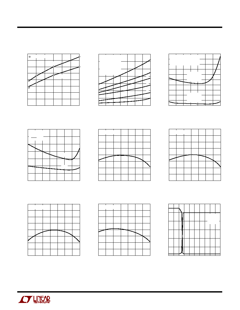
LT1579
TYPICAL PERFOR
M
A
N
CE CHARACTERISTICS
U
W
TEMPERATURE (
°
C)
50
OUTPUT VOLTAGE (V)
3.06
25
1579 G03
3.00
2.96
25
0
50
2.94
2.92
3.08
3.04
3.02
2.98
75
100
125
I
LOAD
= 1mA
Guaranteed Dropout Voltage
OUTPUT CURRENT (mA)
0
0
DROPOUT VOLTAGE (V)
0.1
0.2
0.3
0.4
0.6
0.7
0.8
50
100
150
200
1579 G35
250
300
0.5
= TEST POINTS
T
J
125
°
C
T
J
=
25
°
C
TEMPERATURE (
°
C)
50
4
5
7
25
75
1579 G36
3
2
25
0
50
100
125
1
0
6
QUIESCENT CURRENT (
µ
A)
V
IN1
= 20V
V
IN2
= 6V
V
SHDN
= 0V
I
VIN1
I
VIN2
Quiescent Current in Shutdown
Input Current
V
IN1
V
OUT
(V)
0
INPUT CURRENT (
µ
A)
20
40
60
10
30
50
0
0.2
0.4
0.6
1579 G07
0.8
0.1
0.2
0.1
0.3
0.5
0.7
I
IN2
I
IN1
V
OUT
= 5V
V
IN2
= 6V
I
LOAD
= 0
TEMPERATURE (
°
C)
50
ADJUST PIN VOLTAGE (V)
1.53
25
1579 G05
1.50
1.48
25
0
50
1.47
1.46
1.54
1.52
1.51
1.49
75
100
125
I
LOAD
= 1mA
Adjust Pin Voltage
LT1579-5 Output Voltage
TEMPERATURE (
°
C)
50
OUTPUT VOLTAGE (V)
5.09
25
1579 G05
5.00
4.94
25
0
50
4.91
4.88
5.12
5.06
5.03
4.97
75
100
125
I
LOAD
= 1mA
LT1579-3 Output Voltage
LT1579-3.3 Output Voltage
TEMPERATURE (
°
C)
50
OUTPUT VOLTAGE (V)
3.36
25
1579 G04
3.30
2.26
25
0
50
2.24
2.22
3.38
3.34
3.32
2.28
75
100
125
I
LOAD
= 1mA
Quiescent Current
TEMPERATURE (
°
C)
50
0
QUIESCENT CURRENT (
µ
A)
10
30
40
50
100
0
50
75
1579 G02
20
80
90
60
70
25
25
100
125
V
IN
= 6V
R
L
=
(FIXED)
R
L
= 500k (ADJUSTABLE)
OPERATING
QUIESCENT
CURRENT
STANDBY
QUIESCENT
CURRENT
TEMPERATURE (
°
C)
50
0.4
0.5
0.7
25
75
1579 G01
0.3
0.2
25
0
50
100
125
0.1
0
0.6
DROPOUT VOLTAGE (V)
A: I
LOAD
= 300mA
B: I
LOAD
= 150mA
C: I
LOAD
= 100mA
D: I
LOAD
= 50mA
E: I
LOAD
= 10mA
F: I
LOAD
= 1mA
A
B
C
D
E
F
Dropout Voltage