1
LT1580/LT1580-2.5
s
Low Dropout, 540mV at 7A Output Current
s
Fast Transient Response
s
Remote Sense
s
1mV Load Regulation
s
Fixed 2.5V Output and Adjustable Output
s
No Supply Sequencing Problems in
Dual Supply Mode
The LT Æ1580 is a 7A low dropout regulator designed to
power the new generation of microprocessors. The drop-
out voltage of this device is 100mV at light loads rising to
just 540mV at 7A. To achieve this dropout, a second low
current input voltage 1V greater than the output voltage, is
required. The device can also be used as a single supply
device where dropout is comparable to an LT1584.
Several other new features have been added to the LT1580.
A remote SENSE pin is brought out. This feature virtually
eliminates output voltage variations due to load changes.
Typical load regulation, measured at the SENSE pin, for a
load current step of 100mA to 7A is less than 1mV.
The LT1580 has fast transient response, equal to the
LT1584. On fixed voltage devices, the ADJ pin is brought
out. A small capacitor on the ADJ pin further improves
transient response.
This device is ideal for generating processor supplies of
2V to 3V on motherboards where both 5V and 3.3V
supplies are available.
7A, Very Low
Dropout Regulator
FEATURES
DESCRIPTIO
N
U
, LTC and LT are registered trademarks of Linear Technology Corporation.
Pentium is a registered trademark of Intel Corporation.
PowerPC is a trademark of IBM Corporation.
APPLICATIO
N
S
U
s
Microprocessor Supplies
s
Post Regulators for Switching Supplies
s
High Current Regulators
s
5V to 3.XXV for Pentium
Æ
Processors Operating
at 90MHz to 166MHz and Beyond
s
3.3V to 2.9V for Portable Pentium Processor
s
PowerPC
TM
Series Power Supplies
OUTPUT CURRENT (A)
0
MINIMUM POWER VOLTAGE (V)
1.0
0
1
5
7
1580 G03
4
2
3
6
0.5
DATA SHEET LIMIT
T
J
= 25
∞
C
T
J
= 125
∞
C
INDICATES GUARANTEED TEST POINTS
0
∞
C
T
J
125
∞
C
Dropout Voltage --
Minimum Power Voltage
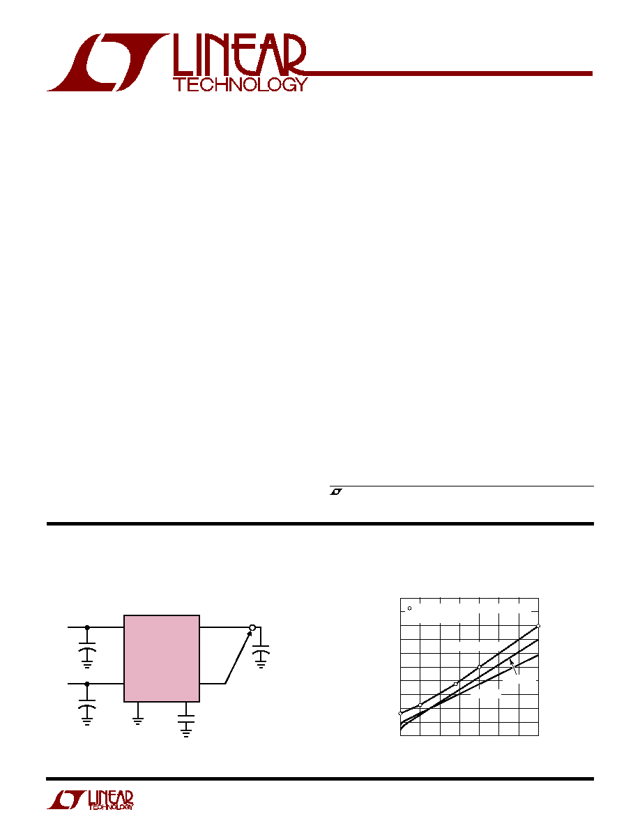
TYPICAL APPLICATIO
N
U
2.5V Microprocessor Supply
V
OUT
SENSE
ADJ
GND
0.1
µ
F
1580 TA01
10
µ
F
TANT
330
µ
F
OS-CON
2.5V/7A
LT1580-2.5
100
µ
F TANT
AVX TPS
◊
7
V
POWER
3.3V
7A
5V
0.2A
V
CONTROL
+
+
+
2
LT1580/LT1580-2.5
ABSOLUTE
M
AXI
M
U
M
RATINGS
W
W
W
U
V
POWER
Input Voltage ................................................ 6V
V
CONTROL
Input Voltage ........................................... 13V
Storage Temperature ............................ ≠ 65
∞
C to 150
∞
C
Operating Junction Temperature Range
Control Section
LT1580C............................................ 0
∞
C to 125
∞
C
LT1580I ........................................ ≠ 40
∞
C to 125
∞
C
Power Transistor
LT1580C ............................................ 0
∞
C to 150
∞
C
LT1580I ........................................ ≠ 40
∞
C to 150
∞
C
Lead Temperature (Soldering, 10 sec) .................. 300
∞
C
PRECO
N
DITIO
N
I
N
G
U
U
U
100% Thermal Limit Functional Test
ELECTRICAL CHARACTERISTICS
(Note 1)
PARAMETER
CONDITIONS
MIN
TYP
MAX
UNITS
Output Voltage: LT1580-2.5
V
CONTROL
= 5V, V
POWER
= 3.3V, I
LOAD
= 0mA
2.485
2.500
2.515
V
V
CONTROL
= 4V to 12V, V
POWER
= 3V to 5.5V, I
LOAD
= 0mA to 4A
q
2.475
2.500
2.525
V
V
CONTROL
= 4V to 12V, V
POWER
= 3V to 5.5V,
2.475
2.500
2.525
V
I
LOAD
= 0mA to 7A, 0
∞
C
T
J
125
∞
C
V
CONTROL
= 4V to 12V, V
POWER
= 3V to 5.5V,
2.460
2.500
2.525
V
I
LOAD
= 0mA to 6.5A, ≠ 40
∞
C
T
J
< 0
∞
C
Reference Voltage: LT1580
V
CONTROL
= 2.75V, V
POWER
= 2V, I
LOAD
= 10mA
1.243
1.250
1.257
V
(V
ADJ
= 0V)
V
CONTROL
= 2.7V to 12V, V
POWER
= 1.75V to 5.5V, I
LOAD
= 10mA to 4A
q
1.237
1.250
1.263
V
V
CONTROL
= 2.7V to 12V, V
POWER
= 2.05V to 5.5V,
1.237
1.250
1.263
V
I
LOAD
= 10mA to 7A, 0
∞
C
T
J
125
∞
C
V
CONTROL
= 2.7V to 12V, V
POWER
= 2.05V to 5.5V,
1.232
1.250
1.263
V
I
LOAD
= 10mA to 6.5A, ≠ 40
∞
C
T
J
< 0
∞
C
Line Regulation: LT1580-2.5
V
CONTROL
= 3.65V to 12V, V
POWER
= 3V to 5.5V, I
LOAD
= 10mA
q
1
3
mV
LT1580
V
CONTROL
= 2.5V to 12V, V
POWER
= 1.75V to 5.5V, I
LOAD
= 10mA
q
1
3
mV
PACKAGE/ORDER I
N
FOR
M
ATIO
N
W
U
U
ORDER PART
NUMBER
ORDER PART
NUMBER
LT1580CT
LT1580IT
LT1580CQ
LT1580IQ
ORDER PART
NUMBER
ORDER PART
NUMBER
LT1580CT7-2.5
LT1580IT7-2.5
LT1580CR-2.5
LT1580IR-2.5
Consult factory for Military grade parts.
JA
= XX
∞
C/ W
R PACKAGE
7-LEAD PLASTIC DD
FRONT VIEW
NC
V
POWER
ADJ
V
OUT
V
CONTROL
GND
SENSE
7
6
5
4
3
2
1
TAB
IS
OUTPUT
JA
= XX
∞
C/ W
Q PACKAGE
5-LEAD PLASTIC DD
TAB
IS
OUTPUT
FRONT VIEW
V
POWER
V
CONTROL
V
OUT
ADJ
SENSE
5
4
3
2
1
JA
= 50
∞
C/ W
T PACKAGE
5-LEAD PLASTIC TO-220
V
POWER
V
CONTROL
V
OUT
ADJ
SENSE
FRONT VIEW
5
4
3
2
1
TAB
IS
OUTPUT
T7 PACKAGE
7-LEAD PLASTIC TO-220
NC
V
POWER
ADJ
V
OUT
V
CONTROL
GND
SENSE
FRONT VIEW
7
6
5
4
3
2
1
TAB
IS
OUTPUT
JA
= 50
∞
C/ W
3
LT1580/LT1580-2.5
ELECTRICAL CHARACTERISTICS
PARAMETER
CONDITIONS
MIN
TYP
MAX
UNITS
Load Regulation: LT1580-2.5
V
CONTROL
= 5V, V
POWER
= 3.3V, I
LOAD
= 0mA to 7A
q
1
5
mV
LT1580 (V
ADJ
= 0V)
V
CONTROL
= 2.75V, V
POWER
= 2.1V, I
LOAD
= 10mA to 7A
q
1
5
mV
Minimum Load Current: LT1580
V
CONTROL
= 5V, V
POWER
= 3.3V, V
ADJ
= 0V (Note 3)
q
5
10
mA
Control Pin Current: LT1580-2.5
V
CONTROL
= 5V, V
POWER
= 3.3V, I
LOAD
= 100mA, 0
∞
C
T
J
125
∞
C
6
10
mA
(Note 4)
V
CONTROL
= 5V, V
POWER
= 3.3V, I
LOAD
= 100mA, ≠ 40
∞
C
T
J
< 0
∞
C
12
mA
V
CONTROL
= 5V, V
POWER
= 3.3V, I
LOAD
= 4A, 0
∞
C
T
J
125
∞
C
30
60
mA
V
CONTROL
= 5V, V
POWER
= 3.3V, I
LOAD
= 4A, ≠ 40
∞
C
T
J
< 0
∞
C
70
mA
V
CONTROL
= 5V, V
POWER
= 3V, I
LOAD
= 4A, 0
∞
C
T
J
125
∞
C
33
70
mA
V
CONTROL
= 5V, V
POWER
= 3V, I
LOAD
= 4A, ≠ 40
∞
C
T
J
< 0
∞
C
80
mA
V
CONTROL
= 5V, V
POWER
= 3.3V, I
LOAD
= 7A, 0
∞
C
T
J
125
∞
C
60
120
mA
V
CONTROL
= 5V, V
POWER
= 3.3V, I
LOAD
= 6.5A, ≠ 40
∞
C
T
J
< 0
∞
C
130
mA
Control Pin Current: LT1580
V
CONTROL
= 2.75V, V
POWER
= 2.05V, I
LOAD
= 100mA, 0
∞
C
T
J
125
∞
C
6
10
mA
(Note 4)
V
CONTROL
= 2.75V, V
POWER
= 2.05V, I
LOAD
= 100mA, ≠ 40
∞
C
T
J
< 0
∞
C
12
mA
V
CONTROL
= 2.75V, V
POWER
= 2.05V, I
LOAD
= 4A, 0
∞
C
T
J
125
∞
C
30
60
mA
V
CONTROL
= 2.75V, V
POWER
= 2.05V, I
LOAD
= 4A, ≠ 40
∞
C
T
J
< 0
∞
C
70
mA
V
CONTROL
= 2.75V, V
POWER
= 1.75V, I
LOAD
= 4A, 0
∞
C
T
J
125
∞
C
33
70
mA
V
CONTROL
= 2.75V, V
POWER
= 1.75V, I
LOAD
= 4A, ≠ 40
∞
C
T
J
< 0
∞
C
80
mA
V
CONTROL
= 2.75V, V
POWER
= 2.05V, I
LOAD
= 7A, 0
∞
C
T
J
125
∞
C
60
120
mA
V
CONTROL
= 2.75V, V
POWER
= 2.05V, I
LOAD
= 6.5A, ≠ 40
∞
C
T
J
< 0
∞
C
130
mA
Ground Pin Current: LT1580-2.5
V
CONTROL
= 5V, V
POWER
= 3.3V, I
LOAD
= 0mA
q
6
10
mA
ADJ Pin Current: LT1580 (V
ADJ
= 0V)
V
CONTROL
= 2.75V, V
POWER
= 2.05V, I
LOAD
= 10mA
q
50
120
µ
A
Current Limit: LT1580-2.5
V
CONTROL
= 5V, V
POWER
= 3.3V,
V
OUT
= 100mV, 0
∞
C
T
J
125
∞
C
7.1
8
A
V
CONTROL
= 5V, V
POWER
= 3.3V,
V
OUT
= 100mV, ≠ 40
∞
C
T
J
< 0
∞
C
6.6
A
LT1580 (V
ADJ
= 0V)
V
CONTROL
= 2.75V, V
POWER
= 2.05V,
V
OUT
= 100mV, 0
∞
C
T
J
125
∞
C
7.1
8
A
V
CONTROL
= 2.75V, V
POWER
= 2.05V,
V
OUT
= 100mV, ≠ 40
∞
C
T
J
< 0
∞
C
6.6
A
Ripple Rejection: LT1580-2.5
V
C
= V
P
= 5V Avg, V
RIPPLE
= 1V
P-P
, I
OUT
= 4A, T
J
= 25
∞
C
60
80
dB
LT1580
V
C
= V
P
= 3.75V Avg, V
RIPPLE
= 1V
P-P
, V
ADJ
= 0V, I
OUT
= 4A, T
J
= 25
∞
C
60
80
dB
Thermal Regulation
30ms Pulse
0.002
0.020
%/W
Thermal Resistance, Junction-to-Case T, T7 Packages, Control Circuitry/Power Transistor
0.65/2.70
∞
C/W
Dropout Voltage (Note 2)
Minimum V
CONTROL
: LT1580-2.5
V
POWER
= 3.3V, I
LOAD
= 100mA, 0
∞
C
T
J
125
∞
C
1.00
1.15
V
(V
CONTROL
≠ V
OUT
)
V
POWER
= 3.3V, I
LOAD
= 100mA, ≠ 40
∞
C
T
J
< 0
∞
C
1.20
V
V
POWER
= 3.3V, I
LOAD
= 1A, 0
∞
C
T
J
125
∞
C
1.00
1.15
V
V
POWER
= 3.3V, I
LOAD
= 1A, ≠ 40
∞
C
T
J
< 0
∞
C
1.20
V
V
POWER
= 3.3V, I
LOAD
= 4A, 0
∞
C
T
J
125
∞
C
1.06
1.20
V
V
POWER
= 3.3V, I
LOAD
= 4A, ≠ 40
∞
C
T
J
< 0
∞
C
1.25
V
V
POWER
= 3.3V, I
LOAD
= 7A, 0
∞
C
T
J
125
∞
C
1.15
1.30
V
V
POWER
= 3.3V, I
LOAD
= 6.5A, ≠ 40
∞
C
T
J
< 0
∞
C
1.35
V
Minimum V
CONTROL
: LT1580
V
POWER
= 2.05V, I
LOAD
= 100mA, 0
∞
C
T
J
125
∞
C
1.00
1.15
V
(V
CONTROL
≠ V
OUT
)
V
POWER
= 2.05V, I
LOAD
= 100mA, ≠ 40
∞
C
T
J
< 0
∞
C
1.20
V
(V
ADJ
= 0V)
V
POWER
= 2.05V, I
LOAD
= 1A, 0
∞
C
T
J
125
∞
C
1.00
1.15
V
V
POWER
= 2.05V, I
LOAD
= 1A, ≠ 40
∞
C
T
J
< 0
∞
C
1.20
V
V
POWER
= 2.05V, I
LOAD
= 2.75A, 0
∞
C
T
J
125
∞
C
1.05
1.18
V
V
POWER
= 2.05V, I
LOAD
= 2.75A, ≠ 40
∞
C
T
J
< 0
∞
C
1.23
V
V
POWER
= 2.05V, I
LOAD
= 4A, 0
∞
C
T
J
125
∞
C
1.06
1.20
V
V
POWER
= 2.05V, I
LOAD
= 4A, ≠ 40
∞
C
T
J
< 0
∞
C
1.25
V
V
POWER
= 2.05V, I
LOAD
= 7A, 0
∞
C
T
J
125
∞
C
1.15
1.30
V
V
POWER
= 2.05V, I
LOAD
= 6.5A, ≠ 40
∞
C
T
J
< 0
∞
C
1.35
V
4
LT1580/LT1580-2.5
PARAMETER
CONDITIONS
MIN
TYP
MAX
UNITS
Minimum V
POWER
: LT1580-2.5
V
CONTROL
= 5V, I
LOAD
= 100mA
q
0.10
0.17
V
(V
POWER
≠ V
OUT
)
V
CONTROL
= 5V, I
LOAD
= 1A
q
0.15
0.22
V
V
CONTROL
= 5V, I
LOAD
= 4A, T
J
= 25
∞
C
0.34
0.40
V
V
CONTROL
= 5V, I
LOAD
= 4A
q
0.50
V
V
CONTROL
= 5V, I
LOAD
= 7A, T
J
= 25
∞
C
0.54
0.62
V
V
CONTROL
= 5V, I
LOAD
= 7A, 0
∞
C
T
J
125
∞
C
0.70
0.80
V
V
CONTROL
= 5V, I
LOAD
= 6.5A, ≠ 40
∞
C
T
J
0
∞
C
0.70
0.80
V
Minimum V
POWER
: LT1580
V
CONTROL
= 2.75V, I
LOAD
= 100mA
q
0.10
0.17
V
(V
POWER
≠ V
OUT
)
V
CONTROL
= 2.75V, I
LOAD
= 1A
q
0.15
0.22
V
(V
ADJ
= 0V)
V
CONTROL
= 2.75V, I
LOAD
2.75A
q
0.26
0.38
V
V
CONTROL
= 2.75V, I
LOAD
= 4A, T
J
= 25
∞
C
0.34
0.40
V
V
CONTROL
= 2.75V, I
LOAD
= 4A
q
0.50
V
V
CONTROL
= 2.75V, I
LOAD
= 7A, T
J
= 25
∞
C
0.54
0.62
V
V
CONTROL
= 2.75V, I
LOAD
= 7A, 0
∞
C
T
J
125
∞
C
0.70
0.80
V
V
CONTROL
= 2.75V, I
LOAD
= 6.5A, ≠ 40
∞
C
T
J
0
∞
C
0.70
0.80
V
ELECTRICAL CHARACTERISTICS
The
q
denotes specifications which apply over the full operating
temperature range.
Note 1: Unless otherwise specified V
OUT
= V
SENSE
. For the LT1580
adjustable device V
ADJ
= 0V.
Note 2: For the LT1580, dropout is caused by either minimum control
voltage (V
CONTROL
) or minimum power voltage (V
POWER
). Both parameters
are specified with respect to the output voltage. The specifications represent
the minimum input/output voltage required to maintain 1% regulation.
Note 3: For the LT1580 adjustable device the minimum load current is the
minimum current required to maintain regulation. Normally the current in
the resistor divider used to set the output voltage is selected to meet the
minimum load current requirement.
Note 4: The control pin current is the drive current required for the output
transistor. This current will track output current with roughly a 1:100 ratio.
The minimum value is equal to the quiescent current of the device.
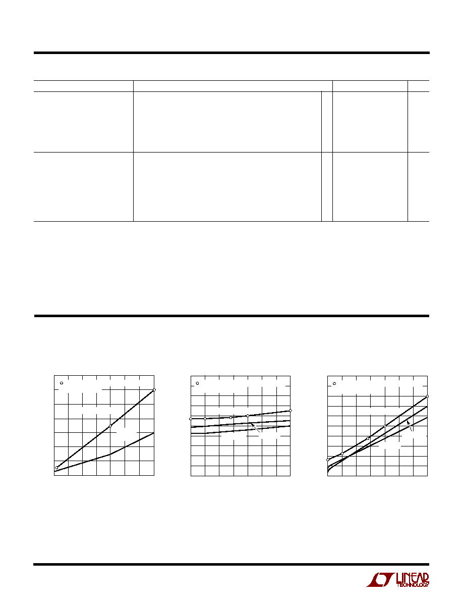
OUTPUT CURRENT (A)
0
MINIMUM POWER VOLTAGE (V)
1.0
0
1
5
7
1580 G03
4
2
3
6
0.5
DATA SHEET LIMIT
T
J
= 25
∞
C
T
J
= 125
∞
C
INDICATES GUARANTEED TEST POINTS
0
∞
C
T
J
125
∞
C
OUTPUT CURRENT (A)
0
MINIMUM CONTROL VOLTAGE
(V
CONTROL
≠ V
OUT
) (V)
2
0
1
5
7
1580 G02
4
2
3
6
1
DATA SHEET LIMIT
T
J
= 25
∞
C
T
J
= 125
∞
C
INDICATES GUARANTEED TEST POINTS
0
∞
C
T
J
125
∞
C
Dropout Voltage --
Minimum Power Voltage
Control Pin Current
vs Output Current
OUTPUT CURRENT (A)
0
140
120
100
80
60
40
20
0
3
5
1580 G01
1
2
4
6
7
CONTROL PIN CURRENT (mA)
DATA SHEET LIMIT
TYPICAL
DEVICE
INDICATES GUARANTEED TEST POINTS
0
∞
C
T
J
125
∞
C
Minimum Control Voltage
TYPICAL PERFOR
M
A
N
CE CHARACTERISTICS
U
W
5
LT1580/LT1580-2.5
TYPICAL PERFOR
M
A
N
CE CHARACTERISTICS
U
W
TEMPERATURE (
∞
C)
≠50 ≠25
OUTPUT VOLTAGE (V)
150
1580 G05
0
25
75
125
50
100
2.508
2.506
2.504
2.502
2.500
2.498
2.496
2.494
2.492
TEMPERATURE (
∞
C)
≠50 ≠25
REFERENCE VOLTAGE (V)
150
1580 G04
0
25
75
125
50
100
1.258
1.256
1.254
1.252
1.250
1.248
1.246
1.244
1.242
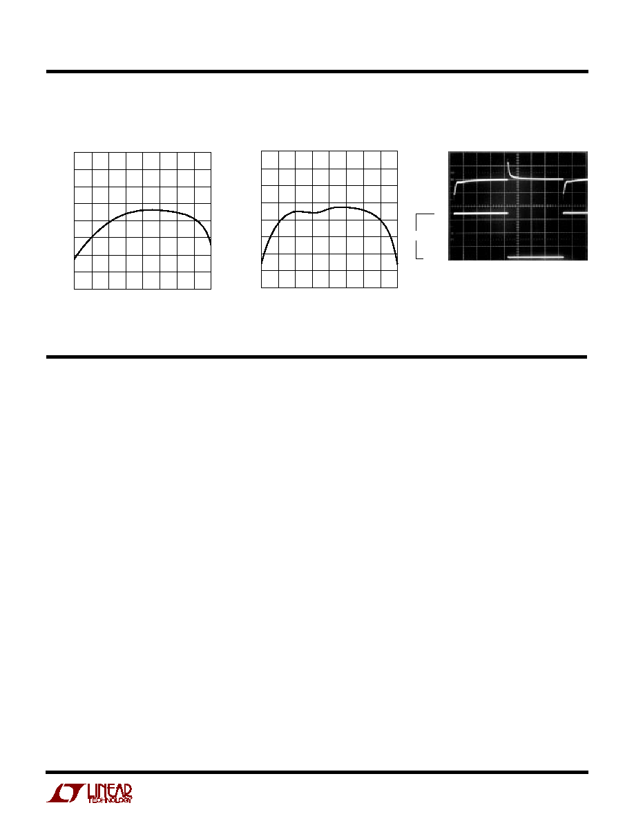
LT1580 Reference Voltage
vs Temperature
400mA
LT1580-2.5 Output Voltage
vs Temperature
7A
V
OUT
50mV/DIV
LOAD
50
µ
s/DIV
1580 TA02
Load Current Step Response
PI
N
FU
N
CTIO
N
S
U
U
U
(5-Lead/7-Lead)
SENSE (Pin 1): This pin is the positive side of the reference
voltage for the device. With this pin it is possible to Kelvin
sense the output voltage at the load.
ADJ (Pin 2/5): This pin is the negative side of the
reference voltage for the device. Transient response can
be improved by adding a small bypass capacitor from the
ADJ pin to ground. For fixed voltage devices the ADJ pin
is also brought out to allow the user to add a bypass
capacitor.
GND (Pin 2, 7-Lead Only): For fixed voltage devices this
is the bottom of the resistor divider that sets the output
voltage.
V
POWER
(Pin 5/6): This is the collector to the power device
of the LT1580. The output load current is supplied through
this pin. For the device to regulate, the voltage at this pin
must be between 0.1V and 0.8V greater than the output
voltage (see Dropout specifications).
V
CONTROL
(Pin 4/3): This pin is the supply pin for the
control circuitry of the device. The current flow into this
pin will be about 1% of the output current. For the device
to regulate, the voltage at this pin must be between 1.0V
and 1.3V greater than the output voltage (see Dropout
specifications).
V
OUT
(Pin 3/4): This is the power output of the device.