Äîêóìåíòàöèÿ è îïèñàíèÿ www.docs.chipfind.ru
1
LT1585-1.5/LT1585A-1.5
Fixed 1.5V, 4.6A and 5A
Low Dropout, Fast Response
GTL+ Regulators
The LT
®
1585-1.5/LT1585A-1.5 are low dropout, 3-termi-
nal regulators with 4.6A and 5A output current capability
respectively, and a fixed 1.5V output voltage. The designs
are optimized for low voltage applications where transient
response and minimum input voltage are critical. Similar to
the LT1084, they have lower dropout and faster transient
response. These improvements make them ideal for low
voltage microprocessor applications, especially as the
regulator in an Intel processor GTL+ supply.
Current limit is trimmed to ensure specified output current
and controlled short-circuit current. On-chip thermal lim-
iting provides protection against any combination of over-
load that creates excessive junction temperatures.
The LT1585-1.5/LT1585A-1.5 are available in the through-
hole 3-pin TO-220 power package and 3-pin plastic DD.
s
Fast Transient Response
s
Guaranteed Dropout Voltage at Multiple Currents
s
Load Regulation: 0.05% Typ
s
Trimmed Current Limit
s
On-Chip Thermal Limiting
s
GTL+ Power Supply
s
Low Voltage Logic Supplies
s
Battery-Powered Circuitry
, LTC and LT are registered trademarks of Linear Technology Corporation.
C3 TO C6
100
µ
F
10V
C1, C2
100
µ
F
10V
+
C7 TO
C12
1
µ
F
R1
75
R5
100
R7
100
R8
100
R6
100
R3
75
R4
150
R2
150
V
REF
V
REF
Q1
Q3
+
3.3V
V
TT
= 1.5V
5A
V
IN
V
OUT
GND
LT1585A-1.5
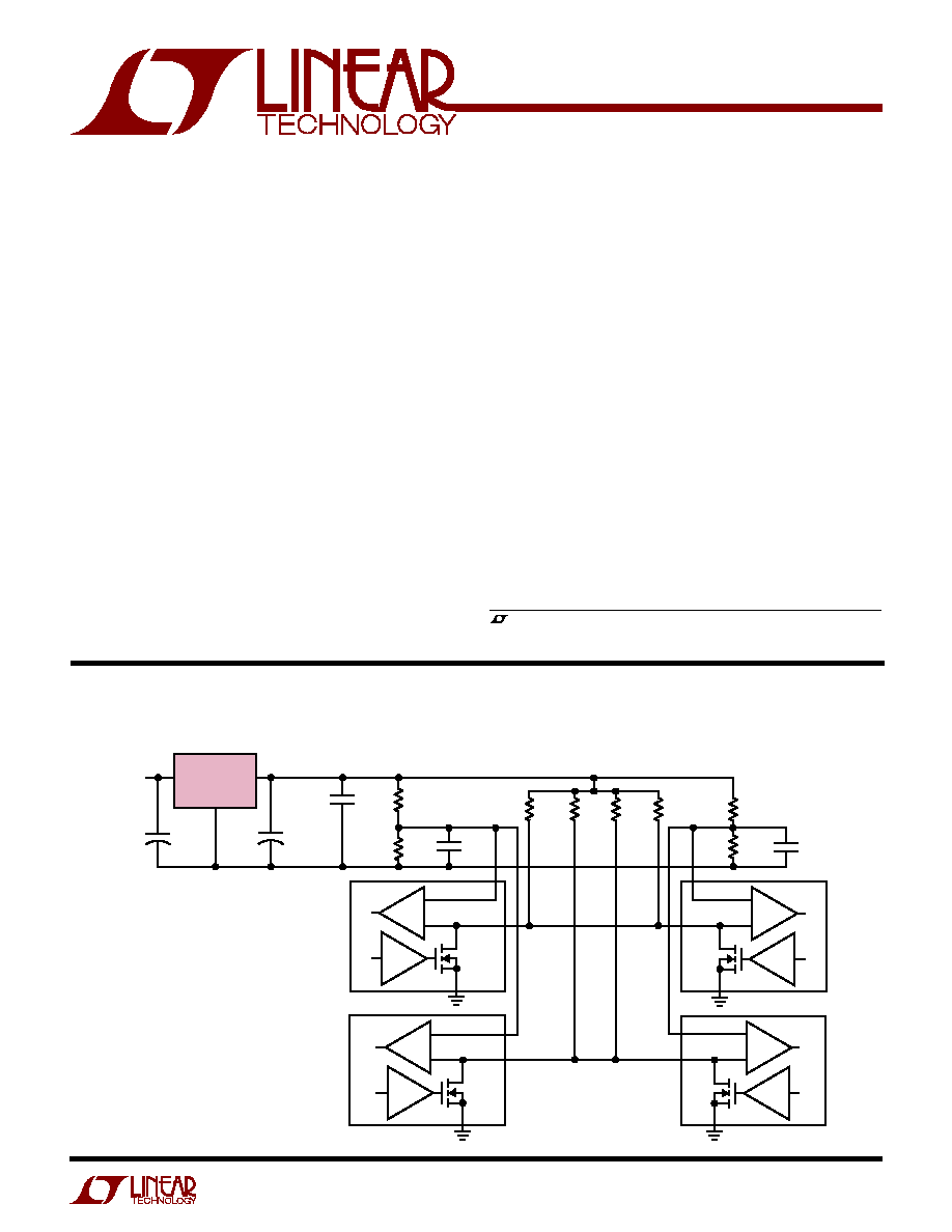
142 TOTAL SIGNAL LINES
·
·
·
C13
0.1
µ
F
Q4
Q2
1585-1.5 · TA01
C14
0.1
µ
F
RX
TX
RX
TX
RX
TX
RX
TX
NOTE: LTC RECOMMENDS CENTRALLY
LOCATING THE LT1585A-1.5 TO MINIMIZE
V
TT
DISTRIBUTION DROPS AND USING
SEPARATE V
REF
GENERATORS AT EACH
BUS END
Intel Processor GTL+ Supply
FEATURES
DESCRIPTIO
U
APPLICATIO S
U
TYPICAL APPLICATIO
U
2
LT1585-1.5/LT1585A-1.5
PACKAGE/ORDER I
N
FOR
M
ATIO
N
W
U
U
ABSOLUTE
M
AXI
M
U
M
RATINGS
W
W
W
U
V
IN
............................................................................ 7V
Operating Junction Temperature Range
Control Section .................................. 0
°
C to 125
°
C
Power Transistor ................................ 0
°
C to 150
°
C
PRECO
N
DITIO
N
I G
U
U
U
100% Thermal Limit Functional Test
T PACKAGE
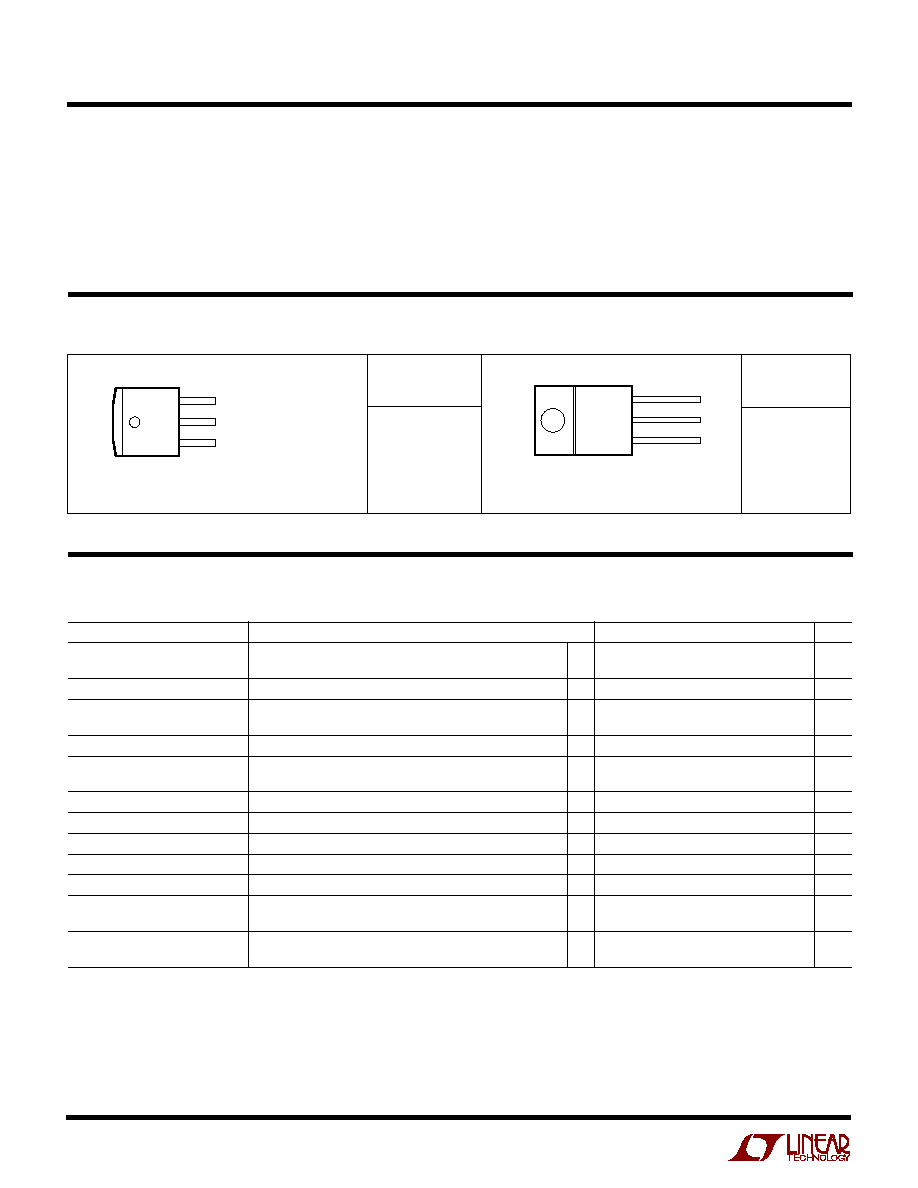
3-LEAD PLASTIC TO-220
FRONT VIEW
3
2
1
TAB IS
OUTPUT
V
IN
V
OUT
GND
JA
= 50
°
C/W
LT1585CT-1.5
LT1585ACT-1.5
ORDER PART
NUMBER
Consult factory for Industrial and Military grade parts.
LT1585CM-1.5
LT1585ACM-1.5
ORDER PART
NUMBER
V
IN
V
OUT
GND
M PACKAGE
3-LEAD PLASTIC DD
FRONT VIEW
TAB
IS
OUTPUT
3
2
1
JA
= 30
°
C/W*
PARAMETER
CONDITIONS
MIN
TYP
MAX
UNITS
Output Voltage (Note 4)
V
IN
= 5V, T
J
= 25
°
C, I
OUT
= 0mA
1.485 ( 1%)
1.5
1.515 (+ 1%)
V
3V
V
IN
7V, 0mA
I
OUT
I
FULL LOAD
q
1.470 ( 2%)
1.5
1.530 (+ 2%)
V
Line Regulation (Notes 2, 3)
3V
V
IN
7V, I
OUT
= 0mA
0.005
0.2
%
Load Regulation
V
IN
= 5V, T
J
= 25
°
C, 0mA
I
OUT
I
FULL LOAD
0.05
0.3
%
(Notes 2, 3, 4)
q
0.05
0.5
%
Dropout Voltage (Note 4)
V
OUT
= 1%, I
OUT
= I
FULL LOAD
q
1.200
1.400
V
Current Limit
LT1585-1.5, (V
IN
V
OUT
) = 5.5V
q
4.60
5.25
A
LT1585A-1.5, (V
IN
V
OUT
) = 5.5V
q
5.00
6.00
A
Quiescent Current
V
IN
= 5V
q
7
13
mA
Ripple Rejection (Note 4)
f = 120Hz, C
OUT
= 25
µ
F Tant., V
IN
= 4.5V, I
OUT
= I
FULL LOAD
q
60
72
dB
Thermal Regulation
T
A
= 25
°
C, 30ms Pulse
0.004
0.02
%/W
Temperature Stability
q
0.5
%
Long-Term Stability
T
A
= 125
°
C, 1000 Hrs.
0.03
1.0
%
RMS Output Noise
T
A
= 25
°
C, 10Hz
f
10kHz
0.003
%
(% of V
OUT
)
Thermal Resistance
T Package: Control Circuitry/Power Transistor
0.7/3.0
°
C/W
Junction to Case
M Package: Control Circuitry/Power Transistor
0.7/3.0
°
C/W
ELECTRICAL CHARACTERISTICS
Note 1: Absolute Maximum Ratings are those values beyond which the life
of the device may be impaired.
Note 2: See thermal regulation specifications for changes in output voltage
due to heating effects. Load and line regulation are measured at a constant
junction temperature by low duty cycle pulse testing.
Note 3: Line and load regulation are guaranteed up to the maximum
power dissipation (25W for the LT1585-1.5 in T package and 27.5W for
the LT1585A-1.5). Power dissipation is determined by input/output
differential and the output current. Guaranteed maximum output power
will not be available over the full input/output voltage range.
Note 4: I
FULL LOAD
is defined as the maximum value of output load current
as a function of input-to-output voltage. I
FULL LOAD
is equal to 4.6A for the
LT1585-1.5 and 5A for the LT1585A-1.5. The LT1585-1.5/LT1585A-1.5
have constant current limit with changes in input-to-output voltage.
*WITH PACKAGE
SOLDERED TO 0.5
SQUARE INCH COPPER
AREA OVER BACKSIDE
GROUND PLANE OR
INTERNAL POWER PLANE.
JA
CAN VARY FROM
20
°
C/W TO > 40
°
C/W
WITH OTHER MOUNTING
TECHNIQUES
The
q
denotes specifications which apply over the specified operating
temperature range, otherwise specifications are at T
A
= 25
°
C.
(Note 1)
Storage Temperature Range ................ 65
°
C to 150
°
C
Lead Temperature (Soldering, 10 sec)................. 300
°
C
3
LT1585-1.5/LT1585A-1.5
TYPICAL PERFOR
M
A
N
CE CHARACTERISTICS
U
W
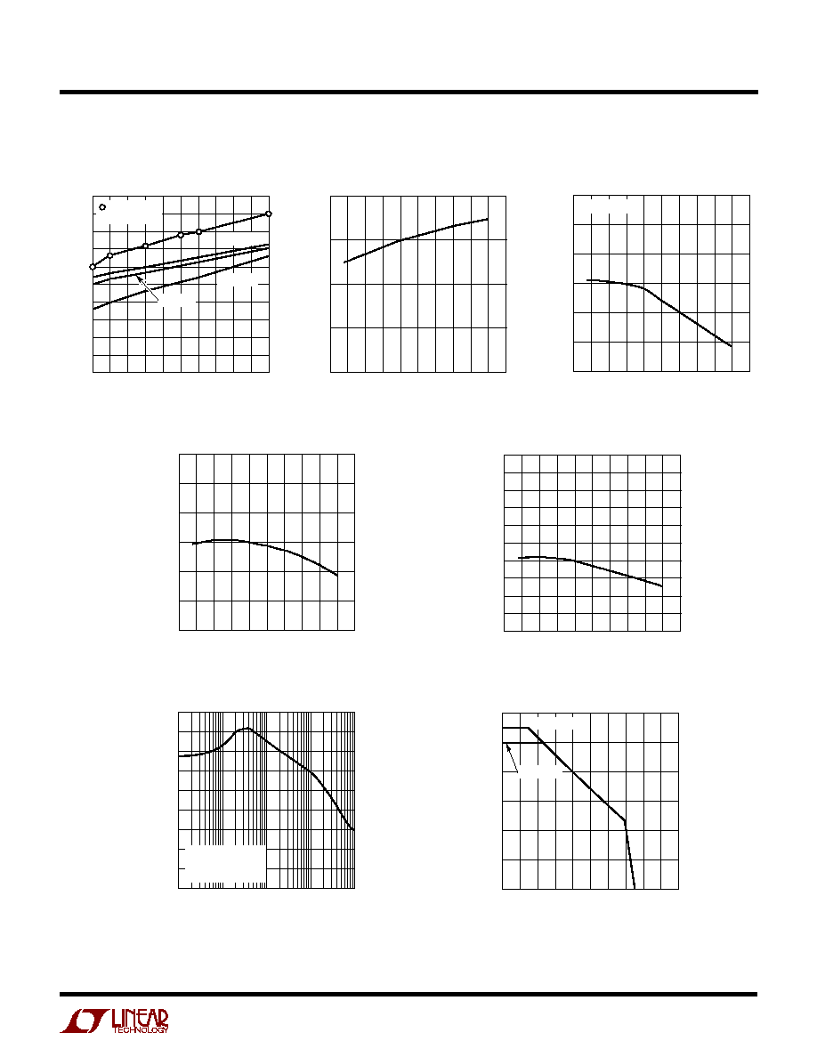
LT1585A-1.5 Short-Circuit Current
vs Temperature
LT1585A-1.5 Dropout Voltage vs
Output Current
OUTPUT CURRENT (A)
0
DROPOUT VOLTAGE (V)
1.1
1.3
1.5
4
1585-1.5 G01
0.9
0.7
1.0
1.2
1.4
0.8
0.6
0.5
1
2
3
5
T = 5
°
C
T = 125
°
C
T = 25
°
C
GUARANTEED
TEST POINTS
TEMPERATURE (
°
C)
75
SHORT-CIRCUIT CURRENT (A)
5.0
5.5
125
1585-1.5 G02
4.5
4.0
25
25 50
175
6.0
75
50
0
150
100
Load Regulation vs Temperature
TEMPERATURE (
°
C)
0.20
OUTPUT VOLTAGE DEVIATION (%)
0.10
0
0.10
0.15
0.05
0.05
25
25
75
125
1585-1.5 G03
175
50
75
0
50
100
150
I = I
FULL LOAD
Output Voltage vs Temperature
Quiescent Current vs Temperature
Ripple Rejection vs Frequency
Maximum Power Dissipation*
*AS LIMITED BY MAXIMUM JUNCTION TEMPERATURE
TEMPERATURE (
°
C)
OUTPUT VOLTAGE (V)
1.53
1.52
1.51
1.50
1.49
1.48
1.47
25
25
75
125
1585-1.5 G04
175
50
75
0
50
100
150
TEMPERATURE (
°
C)
75
QUIESCENT CURRENT (mA)
9
11
13
125
1585-1.5 G05
7
5
8
10
12
6
4
3
25
25
75
50
150
0
50
100
175
FREQUENCY (Hz)
20
RIPPLE REJECTION (dB)
40
50
70
90
10
1k
10k
100k
1585-1.5 G06
0
100
60
30
10
80
(V
IN
V
OUT
)
3V
0.5V
V
RIPPLE
2V
I
OUT
= I
FULL LOAD
CASE TEMPERATURE (°C)
50
POWER (W)
20
25
30
80
100
1585-1.5 G07
15
10
60 70
90
110 120 130 140 150
5
0
LT1585-1.5
LT1585A-1.5
4
LT1585-1.5/LT1585A-1.5
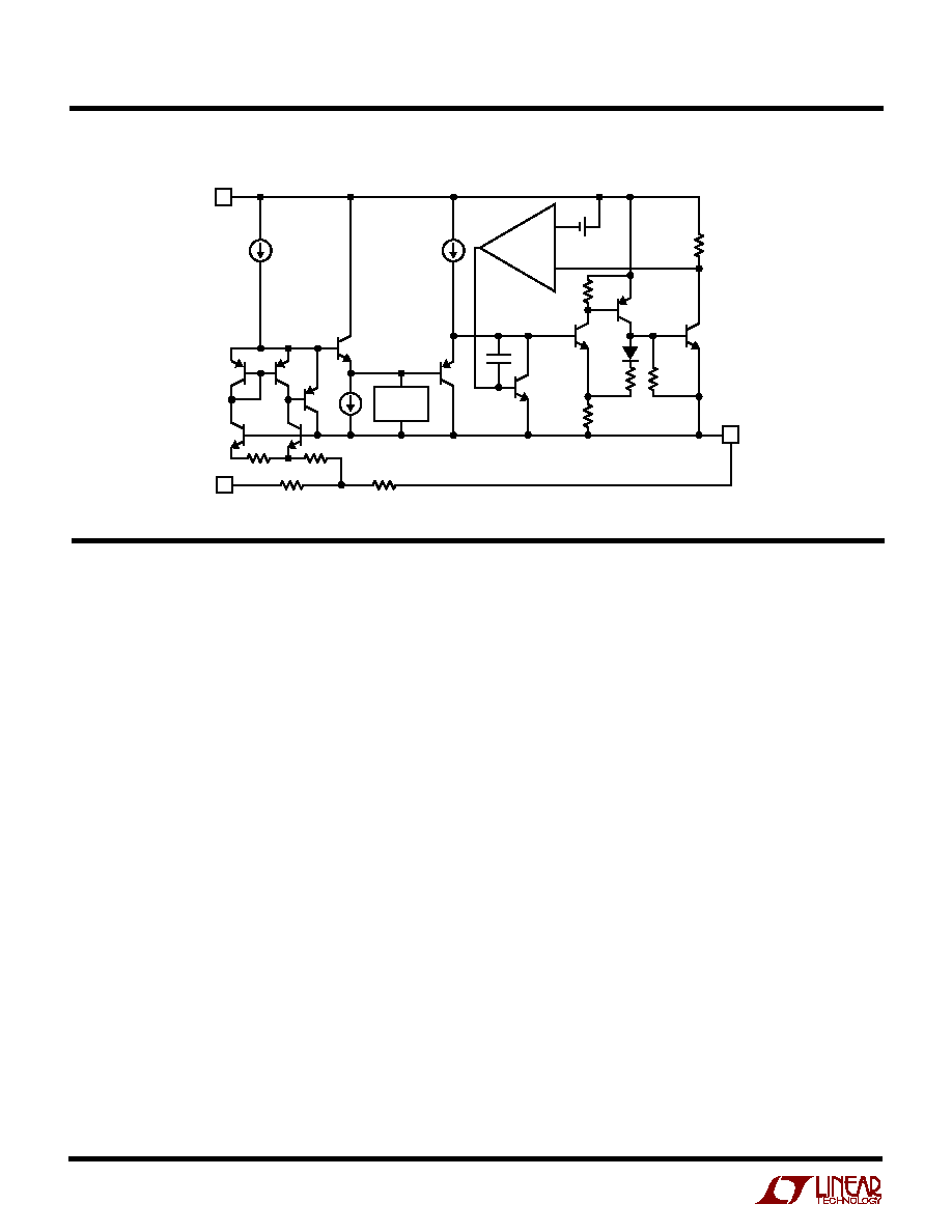
SI PLIFIED SCHE ATIC
W
W
APPLICATIO
N
S I
N
FOR
M
ATIO
N
W
U
U
U
General
The LT1585-1.5/LT1585A-1.5 3-terminal regulators are
easy to use and have all the protection features expected
in high performance linear regulators. The devices are
short-circuit protected, safe-area protected and provide
thermal shutdown to turn off the regulators if the junction
temperature exceeds about 150
°
C.
The ICs are pin compatible with the LT1083/LT1084/LT1085
family of linear regulators but offer lower dropout voltage
and faster transient response. The trade-off for this im-
proved performance is a 7V maximum supply voltage.
Similar to the LT1083/LT1084/LT1085 family, the LT1585-
1.5/LT1585A-1.5 regulators require an output capacitor for
stability. However, the improved frequency compensation
permits the use of capacitors with much lower ESR while still
maintaining stability. This is critical in addressing the needs
of modern low voltage, high speed microprocessors.
Current generation microprocessors and their associated
circuitry cycle load current from almost zero to several
amps in tens of nanoseconds. Output voltage tolerances
are tighter and include transient response as part of the
specification. The LT1585-1.5/LT1585A-1.5 are specifi-
cally designed to meet the fast current load step require-
ments of these applications and save total cost by needing
less output capacitance in order to maintain regulation.
Stability
The circuit design in the LT1585-1.5/LT1585A-1.5 re-
quires the use of an output capacitor as part of the
frequency compensation. For all operating conditions, the
addition of a 22
µ
F solid tantalum or a 100
µ
F aluminum
electrolytic on the output ensures stability. Normally, the
LT1585-1.5/LT1585A-1.5 can use smaller value capaci-
tors. Many different types of capacitors are available and
have widely varying characteristics. These capacitors differ
in capacitor tolerance (sometimes ranging up to
±
100%),
equivalent series resistance, equivalent series inductance
and capacitance temperature coefficient. The LT1585-1.5/
LT1585A-1.5 frequency compensation optimizes frequency
response with low ESR capacitors. In general, use capaci-
tors with an ESR of less than 1
.
Normally, capacitor values on the order of several hundred
microfarads are used on the output of the regulators to
ensure good transient response with heavy load current
changes. Output capacitance can increase without limit
and larger values of output capacitance further improve the
THERMAL
LIMIT
GND
V
IN
V
OUT
1585-1.5 SS
+
5
LT1585-1.5/LT1585A-1.5
APPLICATIO
N
S I
N
FOR
M
ATIO
N
W
U
U
U
stability and transient response of the LT1585-1.5/
LT1585A-1.5.
Large load current changes are exactly the situation pre-
sented by modern microprocessors and their peripheral
circuitry. The load current step contains higher order
frequency components that the output decoupling network
must handle until the regulator throttles to the load current
level. Capacitors are not ideal elements and contain para-
sitic resistance and inductance. These parasitic elements
dominate the change in output voltage at the beginning of
a transient load step change. The ESR of the output
capacitors produces an instantaneous step in output volt-
age [
V =
I(ESR)]. The ESL of the output capacitors
produces a droop proportional to the rate of change of
output current [V = L(
I/
t)]. The output capacitance
produces a change in output voltage proportional to the
time until the regulator can respond [
V =
t(
I/C)]. These
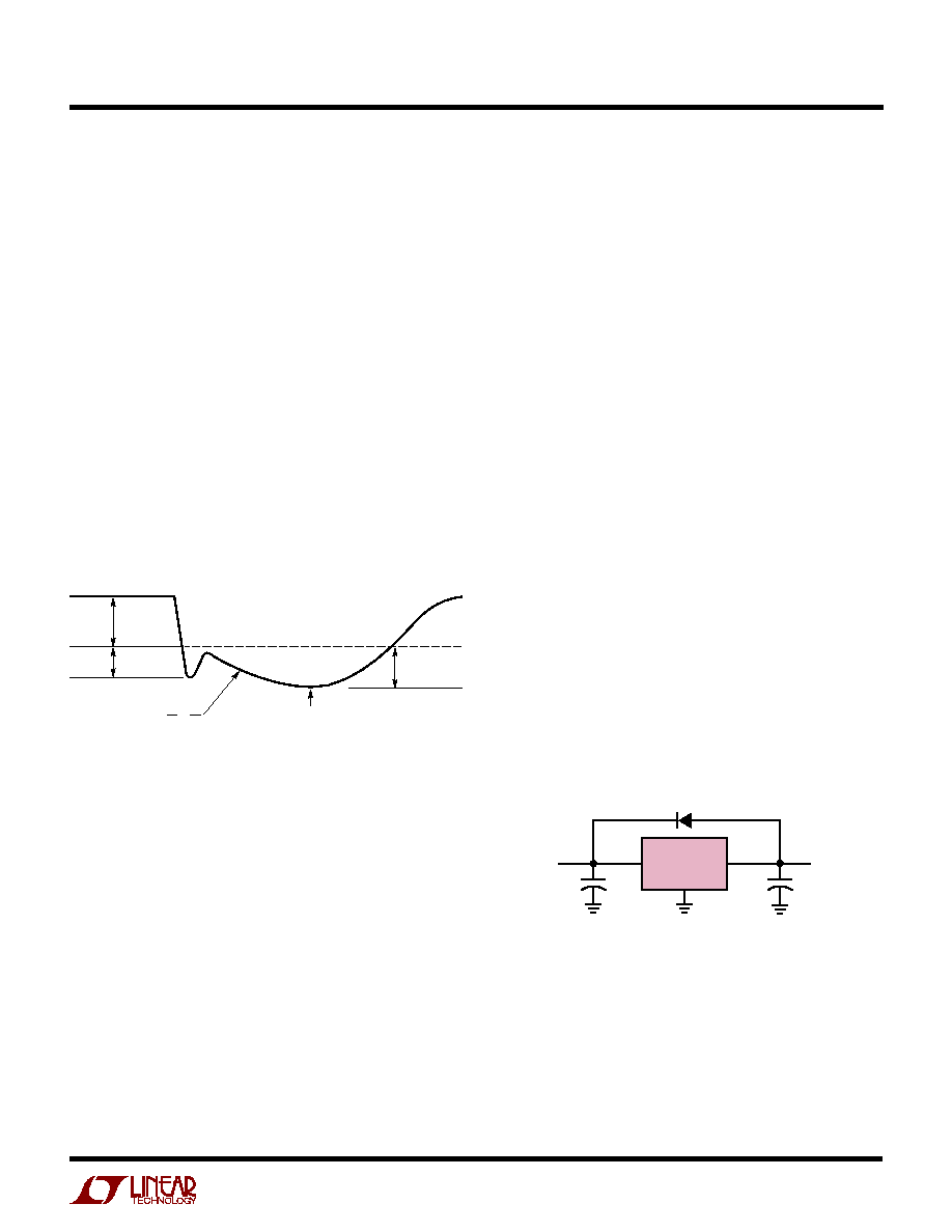
transient effects are illustrated in Figure 1.
range of input supply voltage. The lower current limit rating
and 7V maximum supply voltage rating for this device
permit this characteristic. Current limit oscillations are
typically nonexistent unless the input and output decou-
pling capacitors for the regulators are mounted several
inches from the terminals.
Protection Diodes
In normal operation, the LT1585-1.5/LT1585A-1.5 do not
require any protection diodes. Older 3-terminal regulators
require protection diodes between the output pin and the
input pin to prevent die overstress.
A protection diode between the input and output pins is
usually not needed. An internal diode between the input
and output pins on the LT1585-1.5/LT1585A-1.5 can
handle microsecond surge currents of 50A to 100A. Even
with large value output capacitors it is difficult to obtain
those values of surge currents in normal operation. Only
with large values of output capacitance, such as 1000
µ
F to
5000
µ
F, and with the input pin instantaneously shorted to
ground can damage occur. A crowbar circuit at the input of
the LT1585-1.5/LT1585A-1.5 can generate those levels of
current and a diode from output to input is then recom-
mended. This is shown in Figure 2. Usually, normal power
supply cycling or system "hot plugging and unplugging"
will not generate current large enough to do any damage.
Ripple Rejection
The typical curve for ripple rejection reflects values for the
LT1585-1.5/LT1585A-1.5 as a function of frequency. In
applications that require improved ripple rejection, use the
adjustable LT1585/LT1585A. A bypass capacitor from the
adjust pin to ground reduces the output ripple by the ratio
of V
OUT
/1.25V.
Figure 2
LT1585-1.5
D1
1N4002
(OPTIONAL)
GND
V
IN
V
OUT
IN
OUT
C1
10
µ
F
C2
10
µ
F
1585-1.5 F02
+
+
The use of capacitors with low ESR, low ESL and good high
frequency characteristics is critical in meeting the output
voltage tolerances of these high speed microprocessor
applications. These requirements dictate a combination of
high quality surface mount tantalum capacitors and ce-
ramic capacitors. The location of the decoupling network is
critical to transient response performance. Place the
decoupling network as close as possible to the micropro-
cessor control circuitry because a trace run from the
decoupling capacitors to the actual circuitry is inductive. In
addition, use large power and ground plane areas to
minimize distribution drops.
A possible stability problem that occurs in monolithic linear
regulators is current limit oscillations. The LT1585-1.5/
LT1585A-1.5 essentially have a flat current limit over the
Figure 1
ESR
EFFECTS
1585-1.5 F01
ESL
EFFECTS
CAPACITANCE
EFFECTS
POINT AT WHICH REGULATOR
TAKES CONTROL
SLOPE,
=
V
t
I
C