 | –≠–ª–µ–∫—Ç—Ä–æ–Ω–Ω—ã–π –∫–æ–º–ø–æ–Ω–µ–Ω—Ç: LT1611CS5 | –°–∫–∞—á–∞—Ç—å:  PDF PDF  ZIP ZIP |
1
LT1611
Inverting 1.4MHz Switching
Regulator in SOT-23
s
Very Low Noise: 1mV
P≠P
Output Ripple
s
≠ 5V at 150mA from a 5V Input
s
Better Regulation Than a Charge Pump
s
Effective Output Impedance: 0.14
s
Uses Tiny Capacitors and Inductors
s
Internally Compensated
s
Fixed Frequency 1.4MHz Operation
s
Low Shutdown Current: <1
µ
A
s
Low V
CESAT
Switch: 300mV at 300mA
s
Tiny 5-Lead SOT-23 Package
The LT
Æ
1611 is the industry's first inverting 5-lead SOT-23
current mode DC/DC converter. Intended for use in small,
low power applications, it operates from an input voltage
as low as 1.1V and switches at 1.4MHz, allowing the use
of tiny, low cost capacitors and inductors 2mm or less in
height. Its small size and high switching frequency enable
the complete DC/DC converter function to consume less
than 0.25 square inches of PC board area. Capable of
generating ≠ 5V at 150mA from a 5V supply or ≠ 5V at
100mA from a 3V supply, the LT1611 replaces nonregulated
"charge pump" solutions in many applications.
The LT1611 operates in a dual inductor inverting topology
which filters the input side as well as the output side of the
DC/DC converter. Fixed frequency switching ensures a
clean output free from low frequency noise typically present
with charge pump solutions. No load quiescent current of
the LT1611 is 3mA, while in shutdown quiescent current
drops to 0.5
µ
A. The 36V switch allows V
IN
to V
OUT
differential of up to 33V.
The LT1611 is available in the 5-lead SOT-23 package.
s
MR Head Bias
s
Digital Camera CCD Bias
s
LCD Bias
s
GaAs FET Bias
s
Positive-to-Negative Conversion
V
IN
V
IN
5V
V
OUT
≠5V
150mA
1611 TA01
SW
L1A
22
µ
H
L1B
22
µ
H
D1
GND
LT1611
C1: AVX TAJB226M010
C2: TAIYO YUDEN LMK212BJ105MG
C3: TAIYO YUDEN JMK325BJ226MM (1210 SIZE)
D1: MBR0520
L1: SUMIDA CLS62-220 OR 2
◊
MURATA LQH3C220 (UNCOUPLED)
C1
22
µ
F
C3
22
µ
F
C2
1
µ
F
R2
10k
R1
29.4k
1200pF
NFB
SHDN
+
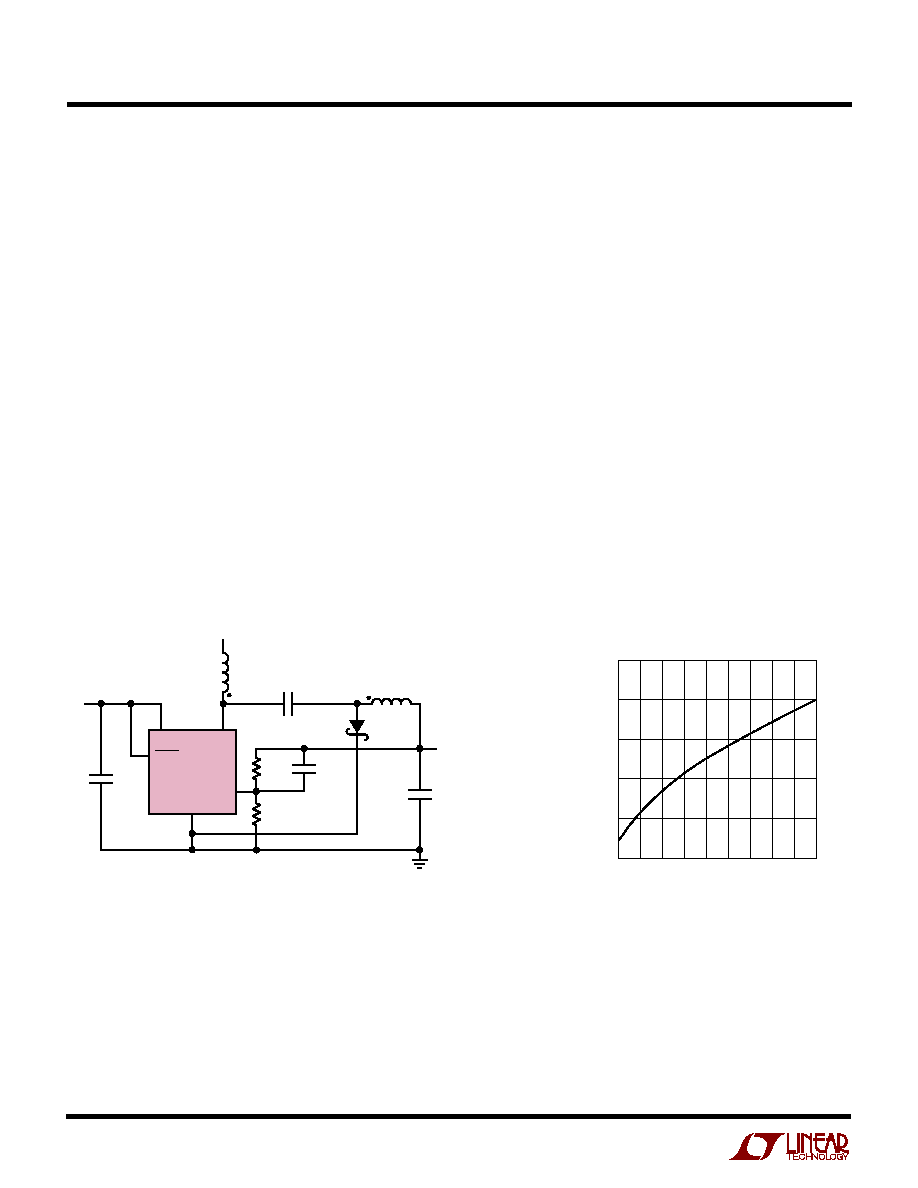
Figure 1. 5V to ≠ 5V, 150mA Low Noise Inverting DC/DC Converter
, LTC and LT are registered trademarks of Linear Technology Corporation.
FEATURES
DESCRIPTIO
U
APPLICATIO S
U
TYPICAL APPLICATIO
U
V
OUT
20mV/DIV
AC COUPLED
LOAD CURRENT
150mA
50mA
100
µ
s/DIV
1611 F10
Transient Response
2
LT1611
ABSOLUTE
M
AXI
M
U
M
RATINGS
W
W
W
U
PACKAGE/ORDER I
N
FOR
M
ATIO
N
W
U
U
ORDER PART
NUMBER
LT1611CS5
T
JMAX
= 125
∞
C,
JA
= 256
∞
C/W
S5 PART MARKING
LTES
Consult factory for Industrial and Military grade parts.
SW 1
GND 2
TOP VIEW
S5 PACKAGE
5-LEAD PLASTIC SOT-23
NFB 3
5 V
IN
4 SHDN
(Note 1)
V
IN
Voltage .............................................................. 10V
SW Voltage ................................................≠ 0.4V to 36V
NFB Voltage ............................................................. ≠ 3V
Current into NFB Pin .............................................
±
1mA
SHDN Voltage .......................................................... 10V
Maximum Junction Temperature .......................... 125
∞
C
Operating Temperature Range
Commercial ............................................. 0
∞
C to 70
∞
C
Extended Commercial (Note 2) ........... ≠ 40
∞
C to 85
∞
C
Storage Temperature Range ................. ≠ 65
∞
C to 150
∞
C
Lead Temperature (Soldering, 10 sec).................. 300
∞
C
ELECTRICAL CHARACTERISTICS
PARAMETER
CONDITIONS
MIN
TYP
MAX
UNITS
Minimum Operating Voltage
0.9
1.1
V
Maximum Operating Voltage
10
V
NFB Pin Bias Current
V
NFB
= ≠1.23V
q
≠ 2.7
≠ 4.7
≠ 6.7
µ
A
Feedback Voltage
q
≠ 1.205
≠ 1.23
≠ 1.255
V
Quiescent Current
V
SHDN
= 1.5V, Not Switching
3
4.5
mA
Quiescent Current in Shutdown
V
SHDN
= 0V, V
IN
= 2V
0.01
0.5
µ
A
V
SHDN
= 0V, V
IN
= 5V
0.01
1.0
µ
A
Reference Line Regulation
1.5V
V
IN
10V
0.02
0.2
%/V
Switching Frequency
q
1.0
1.4
1.8
MHz
Maximum Duty Cycle
q
82
86
%
Switch Current Limit
(Note 3)
550
800
mA
Switch V
CESAT
I
SW
= 300mA
300
350
mV
Switch Leakage Current
V
SW
= 5V
0.01
1
µ
A
SHDN Input Voltage High
1
V
SHDN Input Voltage Low
0.3
V
SHDN Pin Bias Current
V
SHDN
= 3V
25
50
µ
A
V
SHDN
= 0V
0
0.1
µ
A
Note 1: Absolute Maximum Ratings are those values beyond which the life
of a device may be impaired.
Note 2: C grade device specifications are guaranteed over the 0
∞
C to 70
∞
C
temperature range. In addition, C grade device specifications are assured
over the ≠ 40
∞
C to 85
∞
C temperature range by design or correlation, but
are not production tested.
Note 3: Current limit guaranteed by design and/or correlation to static test.
Slope compensation reduces current limit at higher duty cycle.
The
q
denotes the specifications which apply over the full operating
temperature range, otherwise specifications are at T
A
= 25
∞
C. V
IN
= 1.5V, V
SHDN
= V
IN
unless otherwise noted.

3
LT1611
TYPICAL PERFOR A CE CHARACTERISTICS
U
W
LOAD CURRENT (mA)
EFFICIENCY (%)
85
80
75
70
65
60
55
50
1611 G01
0
25
50
75
100
125
150
V
IN
= 3V
V
IN
= 5V
TEMPERATURE (
∞
C)
≠50
0
50
≠25
25
75
100
NFB PIN BIAS CURRENT (
µ
A)
1611 G03
6
5
4
3
2
1
0
SWITCH CURRENT (mA)
0
100
200
300
400
500
600
700
V
CESAT
(mV)
1611 G04
700
600
500
400
300
200
100
0
T
A
= 25
∞
C
SHDN PIN VOLTAGE (V)
0
1
2
3
4
5
SHDN PIN BIAS CURRENT (
µ
A)
1611 G05
50
40
30
20
10
0
DUTY CYCLE (%)
10
SWITCH CURRENT LIMIT (mA)
900
800
700
600
500
400
300
200
100
0
1611 G06
20
30
40
50
60
70
80
T
A
= 25
∞
C
TEMPERATURE (
∞
C)
≠50
≠25
0
25
50
75
100
SWITCHING FREQUENCY (MHz)
1611 G07
2.00
1.75
1.50
1.25
1.00
0.75
0.50
0.25
0
V
IN
= 5V
V
IN
= 1.5V
TEMPERATURE (
∞
C)
≠50
SWITCH CURRENT LIMIT (mA)
900
800
700
600
500
400
300
200
100
0
1611 G09
≠25
0
25
50
75
100
Efficiency, V
OUT
= ≠ 5V
NFB Pin Bias Current vs
Temperature
V
NFB
vs Temperature
Switch V
CESAT
vs Switch Current
Switch Current Limit vs Duty Cycle
SHDN Pin Bias Current vs V
SHDN
Oscillator Frequency vs
Temperature
Switch Current Limit vs
Temperature (Duty Cycle = 30%)
No-Load Operating Quiescent
Current vs Temperature*
TEMPERATURE (
∞
C)
≠50
0
50
≠25
25
75
100
V
NFB
(V)
1611 G02
≠1.245
≠1.240
≠1.235
≠1.230
≠1.225
≠1.220
≠1.215
≠1.210
TEMPERATURE (
∞
C)
≠50
0
50
≠25
25
75
100
OPERATING CURRENT (mA)
1611 G08
6.0
5.5
5.0
4.5
4.0
3.5
3.0
2.5
2.0
* Includes bias current through R1, R2 and Schottky leakage current at T
75
∞
C
4
LT1611
PI
N
FU
N
CTIO
N
S
U
U
U
SW (Pin 1): Switch Pin. Minimize trace area at this pin to
keep EMI down.
GND (Pin 2): Ground. Tie directly to local ground plane.
NFB (Pin 3): Negative Feedback Pin. Minimize trace area.
Reference voltage is ≠1.23V. Connect resistive divider tap
here. The suggested value for R2 is 10k. Set R1 and R2
according to:
R
V
R
OUT
1
1 23
1 23
2
4 5 10
6
=
-
+
-
.
.
. ∑
SHDN (Pin 4): Shutdown Pin. Tie to 1V or more to enable
device. Ground to shut the device down.
V
IN
(Pin 5): Input Supply Pin. Must be locally bypassed.
BLOCK DIAGRA
M
W
≠
+
≠
+
FF
R
Q
S
0.15
SW
DRIVER
COMPARATOR
2
SHUTDOWN
SHDN
4
1
≠
+
RAMP
GENERATOR
R
C
C
C
1.4MHz
OSCILLATOR
GND
1611 BD
R6
40k
R4
140k
R3
30k
Q2
x10
Q1
Q3
R5
40k
V
IN
V
IN
5
NFB
C
PL
(OPTIONAL)
R2
(EXTERNAL)
R1
(EXTERNAL)
V
OUT
NFB
3
A2
A = 3
A1
g
m
OPERATIO
U
The LT1611 combines a current mode, fixed frequency
PWM architecture with a ≠1.23V reference to directly
regulate negative outputs. Operation can be best under-
stood by referring to the block diagram of Figure 2. Q1 and
Q2 form a bandgap reference core whose loop is closed
around the output of the converter. The driven reference
point is the lower end of resistor R4, which normally sits
at a voltage of ≠1.23V. As the load current changes, the
NFB pin voltage also changes slightly, driving the output
of g
m
amplifier A1. Switch current is regulated directly on
a cycle-to-cycle basis by A1's output. The flip-flop is set at
the beginning of each cycle, turning on the switch. When
the summation of a signal representing switch current and
a ramp generator (introduced to avoid subharmonic oscil-
lations at duty factors greater than 50%) exceeds the V
C
signal, comparator A2 changes stage, resetting the flip-
Figure 2
flop and turning off the switch. Output voltage decreases
(the magnitude increases) as switch current is increased.
The output, attenuated by external resistor divider R1 and
R2, appears at the NFB pin, closing the overall loop.
Frequency compensation is provided internally by R
C
and
C
C
. Transient response can be optimized by the addition of
a phase lead capacitor, C
PL
, in parallel with R1 in applica-
tions where large value or low ESR output capacitors are
used.
As load current is decreased, the switch turns on for a
shorter period each cycle. If the load current is further
decreased, the converter will skip cycles to maintain
output voltage regulation.
The LT1611 can work in either of two topologies. The
simpler topology appends a capacitive level shift to a
5
LT1611
OPERATIO
U
boost converter, generating a negative output voltage,
which is directly regulated. The circuit schematic is de-
tailed in Figure 3. Only one inductor is required, and the
two diodes can be in a single SOT-23 package. Output
noise is the same as in a boost converter, because current
is delivered to the output only during the time when the
LT1611's internal switch is off.
If D2 is replaced by an inductor, as shown in Figure 4, a
higher performance solution results. This converter topol-
ogy was developed by Professor S. Cuk of the California
Institute of Technology in the 1970s. A low ripple voltage
results with this topology due to inductor L2 in series with
the output. Abrupt changes in output capacitor current are
eliminated because the output inductor delivers current to
the output during both the off-time and the on-time of the
LT1611 switch. With proper layout and high quality output
capacitors, output ripple can be as low as 1mV
P≠P
.
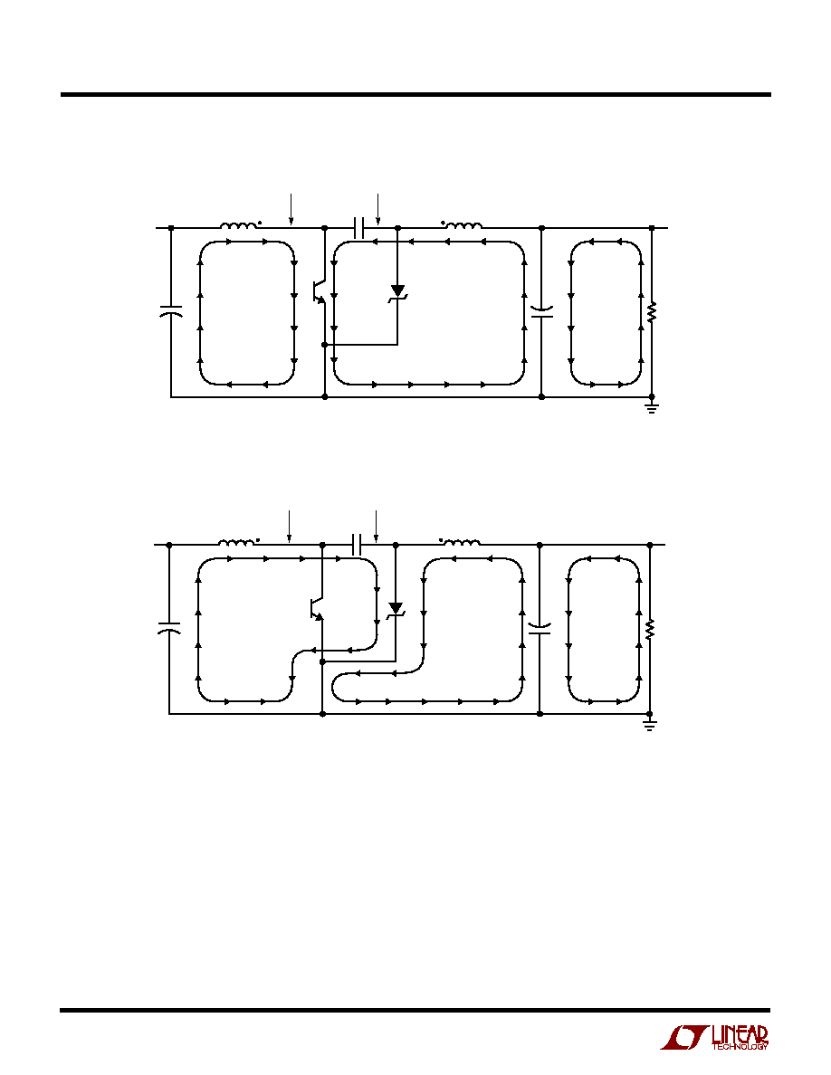
The operation of Cuk's topology is shown in Figures 5
and 6. During the first switching phase, the LT1611's
switch, represented by Q1, is on. There are two current
loops in operation. The first loop begins at input capacitor
C1, flows through L1, Q1 and back to C1. The second loop
flows from output capacitor C3, through L2, C2, Q1 and
back to C3. The output current from R
LOAD
is supplied by
L2 and C3. The voltage at node SW is V
CESAT
and at node
SWX the voltage is ≠(V
IN
+ |V
OUT
|). Q1 must conduct both
L1 and L2 current. C2 functions as a voltage level shifter,
with an approximately constant voltage of (V
IN
+ |V
OUT
|)
across it.
When Q1 turns off during the second phase of switching,
the SW node voltage abruptly increases to (V
IN
+ |V
OUT
|).
The SWX node voltage increases to V
D
(about 350mV).
Now current in the first loop, begining at C1, flows through
L1, C2, D1 and back to C1. Current in the second loop flows
from C3 through L2, D1 and back to C3. Load current
continues to be supplied by L2 and C3.
An important layout issue arises due to the chopped
nature of the currents flowing in Q1 and D1. If they are both
tied directly to the ground plane before being combined,
switching noise will be introduced into the ground plane.
It is almost impossible to get rid of this noise, once present
in the ground plane. The solution is to tie D1's cathode to
the ground pin of the LT1611 before the combined cur-
rents are dumped into the ground plane as drawn in
Figures 4, 5 and 6. This single layout technique can
virtually eliminate high frequency "spike" noise so often
present on switching regulator outputs.
Output ripple voltage appears as a triangular waveform
riding on V
OUT
. Ripple magnitude equals the ripple current
of L2 multiplied by the equivalent series resistance (ESR)
of output capacitor C3. Increasing the inductance of L1
and L2 lowers the ripple current, which leads to lower
output voltage ripple. Decreasing the ESR of C3, by using
ceramic or other low ESR type capacitors, lowers output
ripple voltage. Output ripple voltage can be reduced to
arbitrarily low levels by using large value inductors and
low ESR, high value capacitors.
V
IN
V
IN
≠V
OUT
1611 F03
SW
L1
D1
D2
GND
LT1611
C1
C3
C2
1
µ
F
R2
10k
R1
NFB
SHDN
SHUTDOWN
+
+
V
IN
V
IN
≠V
OUT
1611 F04
SW
L1
L2
D1
GND
LT1611
C1
C3
C2
1
µ
F
R2
10k
R1
NFB
+
+
Figure 3. Direct Regulation of Negative Output
Using Boost Converter with Charge Pump
Figure 4. L2 Replaces D2 to Make Low Output Ripple
Inverting Topology. Coupled or Uncoupled Inductors Can
Be Used. Follow Phasing If Coupled for Best Results
6
LT1611
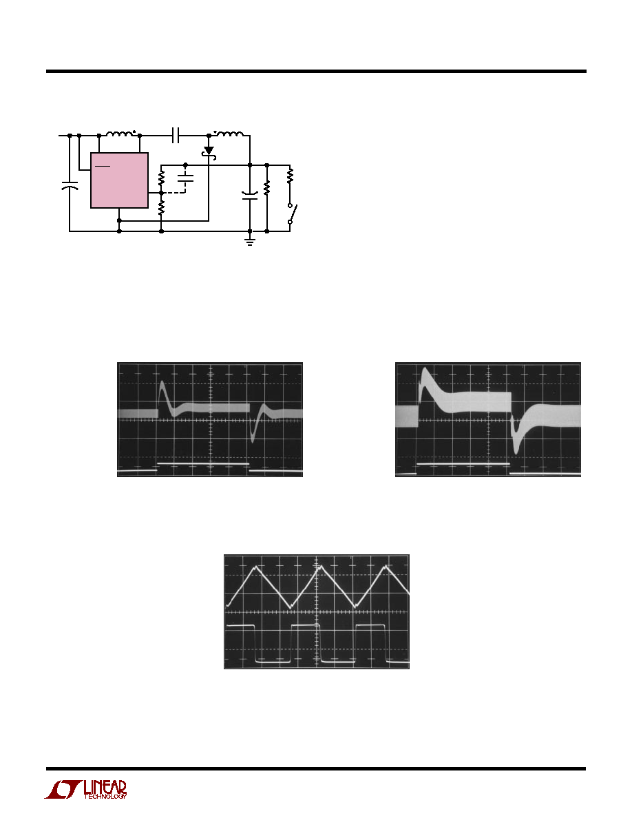
Transient Response
The inverting architecture of the LT1611 can generate a
very low ripple output voltage. Recently available high
value ceramic capacitors can be used successfully in
LT1611 designs with the addition of a phase lead capaci-
tor, C
PL
(see Figure 7). Connected in parallel with feedback
resistor R1, this capacitor reduces both output perturba-
OPERATIO
U
tions due to load steps and output ripple voltage to very
low levels. To illustrate, Figure 7 shows an LT1611 invert-
ing converter with resistor loads R
L1
and R
L2
.
R
L1
is
connected across the output, while R
L2
is switched in
externally via a pulse generator. Output voltage wave-
forms are pictured in subsequent figures, illustrating the
performance of output capacitor type and the effect of C
PL
connected across R1.
+
+
L1
L2
C2
≠(V
IN
+
V
OUT
)
SW
SWX
D1
Q1
1611 F05
C1
C3
R
LOAD
≠V
OUT
V
IN
V
CESAT
+
+
L1
L2
C2
V
IN
+
V
OUT
+ V
D
SW
SWX
D1
Q1
1611 F06
C1
C3
R
LOAD
≠V
OUT
V
IN
V
D
Figure 5. Switch-On Phase of Inverting Converter. L1 and L2 Current Have Positive dI/dt
Figure 6. Switch-Off Phase of Inverting Converter. L1 and L2 Current Have Negative dI/dt
7
LT1611
Figure 8 shows the output voltage with a 50mA to 150mA
load step, using an AVX TAJ "B" case 22
µ
F tantalum
capacitor at the output. Output perturbation is approxi-
mately 100mV as the load changes from 50mA to 150mA.
Steady-state ripple voltage is 20mV
P≠P
, due to L1's ripple
current and C3's ESR. Step response can be improved by
adding a 3.3nF capacitor (C
PL
) as shown in Figure 9.
Settling time improves from 150
µ
s to 40
µ
s, although
steady-state ripple voltage does not improve. Figure 10
pictures the output voltage and switch pin voltage at
200ns per division. Note the absence of high frequency
spikes at the output. This is easily repeatable with proper
layout, described in the next section.
OPERATIO
U
V
IN
V
IN
5V
≠V
OUT
1611 F07
SW
L1A
22
µ
H
L1B
22
µ
H
D1
GND
LT1611
C1: AVX TAJB226M010
C2: TAIYO YUDEN LMK212BJ105MG
C3: SEE TEXT
D1: MBR0520
L1A, L1B: SUMIDA CLS62-220
C1
C3
C2
1
µ
F
R2
10k
R1
C
PL
NFB
SHDN
+
+
R
L1
100
R
L2
50
Figure 7. Switching R
L2
Provides 50mA to 150mA
Load Step for LT1611 5V to ≠ 5V Converter
Figure 8. Load Step Response of LT1611
with 22
µ
F Tantalum Output Capacitor
Figure 9. Addition of C
PL
to Figure 7's Circuit
Improves Load Step Response. C
PL
= 3.3nF
Figure 10. 22
µ
F "B" Case Tantalum Capacitor (AVX TAJ "B" Series)
Has ESR Resulting in 20mV
P≠P
Voltage Ripple at Output
V
OUT
50mV/DIV
AC COUPLED
LOAD CURRENT
150mA
50mA
100
µ
s/DIV
1611 F08
V
OUT
20mV/DIV
AC COUPLED
LOAD CURRENT
150mA
50mA
20
µ
s/DIV
1611 F09
V
OUT
10mV/DIV
SWITCH VOLTAGE
5V/DIV
LOAD = 150mA
200ns/DIV
1611 F10
8
LT1611
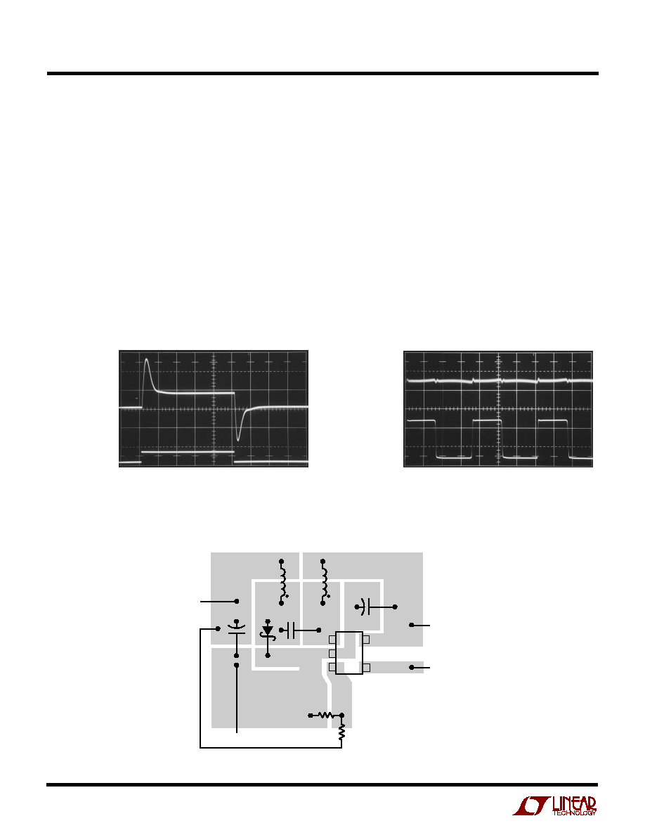
In Figure 11 (also shown on the first page), output capaci-
tor C3 is replaced by a ceramic unit. These large value
ceramic capacitors have ESR of about 2m
and result in
very low output ripple. At the 20mV/division scale, output
voltage ripple cannot be seen. Figure 12 pictures the
output and switch nodes at 200ns per division. The output
voltage ripple is approximately 1mV
P≠P
. Again, good
layout is mandatory to achieve this level of performance.
OPERATIO
U
Layout
The LT1611 switches current at high speed, mandating
careful attention to layout for best performance.
You will
not get advertised performance with careless layout. Figure 13
shows recommended component placement. Follow this
closely in your printed circuit layout. The cut ground
copper at D1's cathode is essential to obtain the low noise
achieved in Figures 11 and 12's oscillographs. Input
bypass capacitor C1 should be placed close to the LT1611
as shown. The load should connect directly to output
capacitor C2 for best load regulation. You can tie the local
ground into the system ground plane at C3's ground
terminal.
Figure 11. Replacing C3 with 22
µ
F Ceramic Capacitor
(Taiyo Yuden JMK325BJ226MM) Improves Output
Noise. C
PL
= 1200pF Results in Best Phase Margin
V
OUT
20mV/DIV
AC COUPLED
LOAD CURRENT
150mA
50mA
100
µ
s/DIV
1611 F11
Figure 12. 22
µ
F Ceramic Capacitor at
Output Reduces Ripple to 1mV
P≠P
. Proper
Layout Is Essential to Achieve Low Noise
V
OUT
5mV/DIV
AC COUPLED
SWITCH VOLTAGE
5V/DIV
LOAD = 150mA
200ns/DIV
1611 F12
Figure 13. Suggested Component Placement. Note Cut in Ground Copper at D1's Cathode
1
2
3
5
4
C2
D1
R2
R1
L1B
C1
L1A
+
+
SHUTDOWN
1611 F13
≠V
OUT
GND
V
IN
C3
9
LT1611
OPERATIO
U
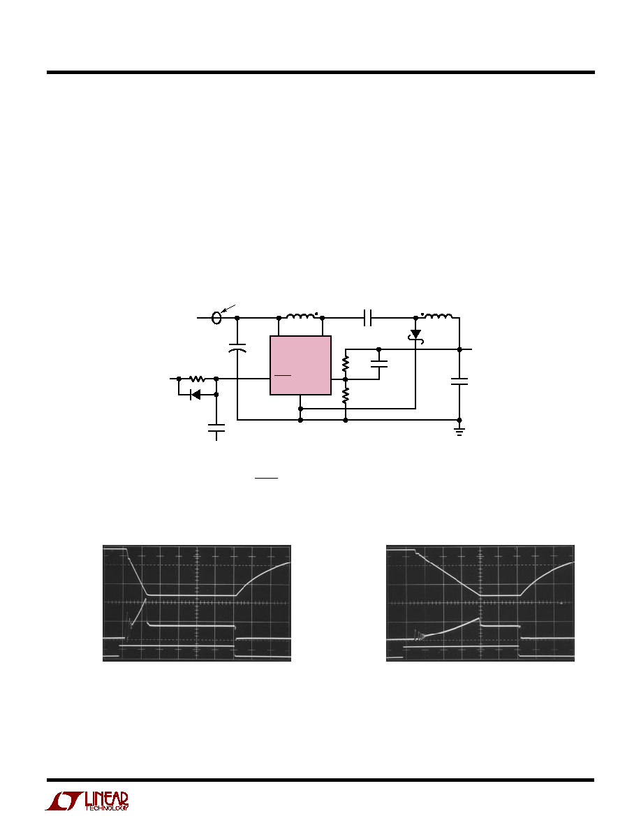
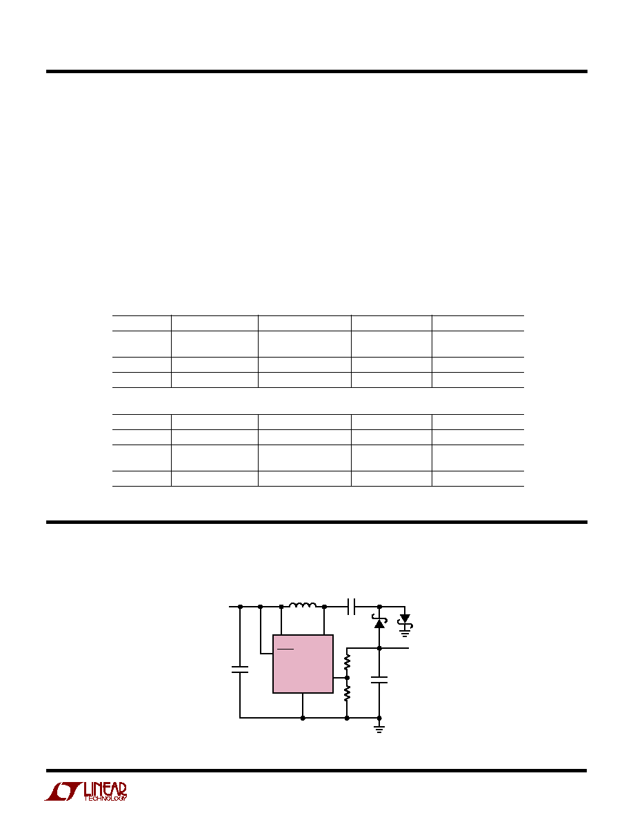
Start-Up/Soft-Start
The LT1611, starting from V
OUT
= 0V, reaches final voltage
in approximately 450
µ
s after SHDN is pulled high, with
C
OUT
= 22
µ
F, V
IN
= 5V and V
OUT
= ≠ 5V. Charging the output
capacitor at this speed requires an inrush current of over
1A. If a longer start-up time is acceptable, a soft-start
circuit consisting of R
SS
and C
SS
, as shown in Figure 14,
can be used to limit inrush current to a lower value. Figure
15 pictures V
OUT
and input current, starting into a 33
load, with R
SS
of 33k
and C
SS
of 33nF. Input current,
V
IN
V
IN
5V
V
SS
V
OUT
V
OUT
≠5V
1611 F14
SW
L1A
22
µ
H
CURRENT
PROBE
L1B
22
µ
H
D1
GND
LT1611
C1: AVX TAJB226M010
C2: TAIYO YUDEN LMK212BJ105MG
C3: TAIYO YUDEN JMK325BJ226MM (1210 SIZE)
D1: MBR0520
L1: SUMIDA CLS62-220 OR 2
◊
MURATA LQH3C220 (UNCOUPLED)
C1
22
µ
F
R
SS
33k
D2
1N4148
C3
22
µ
F
C2
1
µ
F
R2
10k
R1
29.4k
C
P
1200pF
NFB
SHDN
+
C
SS
33nF/0.1
µ
F
Figure 14. R
SS
and C
SS
at SHDN Pin Provide Soft-Start to LT1611 Inverting Converter
measured at V
IN
, is limited to a peak value of 450mA as the
time required to reach final value increases to 700
µ
s. In
Figure 16, C
SS
is increased to 0.1
µ
F, resulting in a lower
peak input current of 240mA with a V
OUT
ramp time of
2.1ms. C
SS
can be increased further for an even slower
ramp, if desired. Diode D2 serves to quickly discharge C
SS
when V
SS
is driven low to shut down the device. D2 can be
omitted, resulting in a "soft-stop" slow discharge of the
output capacitor.
Figure 15. R
SS
= 33k, C
SS
= 33nF; V
OUT
Reaches
≠ 5V in 750
µ
s; Input Current Peaks at 450mA
V
OUT
2V/DIV
I
IN
200mA/DIV
LOAD = 150mA
500
µ
s/DIV
1611 F15
V
S
5V/DIV
Figure 16. R
SS
= 33k, C
SS
= 0.1
µ
F; V
OUT
Reaches
≠ 5V in 2.1ms; Input Current Peaks at 240mA
V
OUT
2V/DIV
I
IN
200mA/DIV
LOAD = 150mA
500
µ
s/DIV
1611 F16
V
S
5V/DIV
10
LT1611
OPERATIO
U
Output Current
The LT1611 will deliver 150mA at ≠ 5V from a 5V
±
10%
input supply. If a higher voltage supply is available, more
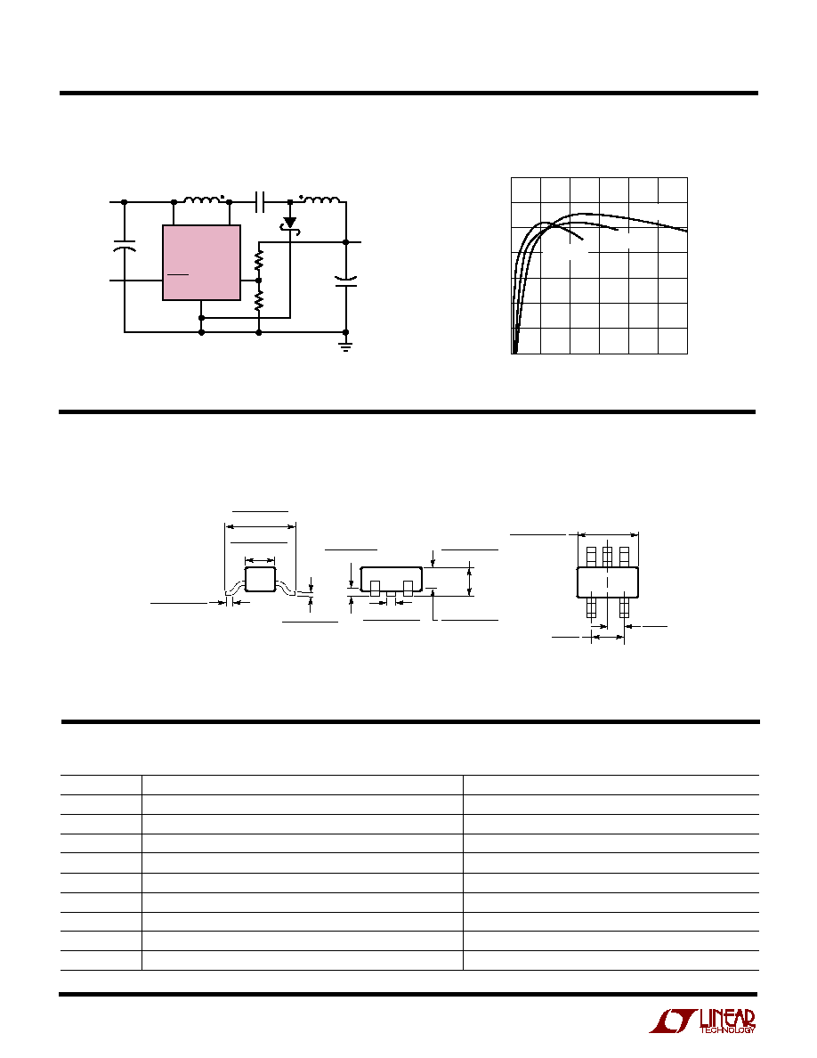
output current can be obtained. Figure 17's schematic
shows how to get more current. Although the LT1611's
maximum voltage allowed at V
IN
is 10V, the SW pin can
handle higher voltage (up to 36V). In Figure 17, the V
IN
pin
of the LT1611 is driven from a 5V supply, while input
inductor L
1A
is driven from a separate 12V supply. Figure
18's graph shows maximum recommended output cur-
rent as the voltage on L
1A
is varied. Up to 300mA can be
delivered when driving L
1A
from a 12V supply.
COMPONENT SELECTION
Inductors
Each of the two inductors used with the LT1611 should
have a saturation current rating (where inductance is
approximately 70% of zero current inductance) of ap-
proximately 0.25A or greater. If the device is used in
"charge pump" mode, where there is only one inductor,
then its rating should be 0.5A or greater. DCR of the
inductors should be 0.5
or less. A value of 22
µ
H is
suitable if using a coupled inductor such as Sumida
CLS62-220 or Coiltronics CTX20-1. If using two separate
inductors, increasing the value to 47
µ
H will result in the
same ripple current. Inductance can be reduced if operat-
ing from a supply voltage below 3V. Table 1 lists several
inductors that will work with the LT1611, although this is
not an exhaustive list. There are many magnetics vendors
whose components are suitable.
V
IN
5V
V
OUT
≠5V
UP TO 300mA
1611 F17
SW
L1A
22
µ
H
L1B
22
µ
H
D1
GND
LT1611
C1, C2: TAIYO YUDEN LMK212BJ105MG
C3: TAIYO YUDEN JMK325BJ226MM
D1: MBR0520
L1A, L1B: SUMIDA CLS62-220
C1
1
µ
F
C3
22
µ
F
C2
1
µ
F
V
L
(SEE TEXT)
10k
29.4k
1200pF
NFB
SHDN
V
L
(V)
3
4
5
6
7
8
9
10
11
12
MAXIMUM RECOMMENDED
OUTPUT CURRENT (mA)
1611 F18
350
300
250
200
150
100
Figure 17. Increase Output Current By Driving L1A from a Higher Voltage
Figure 18. Output Current Increases to
300mA When Driving V
L
from 12V Supply
11
LT1611
TYPICAL APPLICATIO S
U
Information furnished by Linear Technology Corporation is believed to be accurate and reliable.
However, no responsibility is assumed for its use. Linear Technology Corporation makes no represen-
tation that the interconnection of its circuits as described herein will not infringe on existing patent rights.
Table 1. Inductor Vendors
VENDOR
PHONE
URL
PART
COMMENT
Sumida
(847) 956-0666
www.sumida.com
CLS62-22022
22
µ
H Coupled
CD43-470
47
µ
H
Murata
(404) 436-1300
www.murata.com
LQH3C-220
22
µ
H, 2mm Height
Coiltronics
(407) 241-7876
www.coiltronics.com
CTX20-1
20
µ
H Coupled, Low DCR
Table 2. Capacitor Vendors
VENDOR
PHONE
URL
PART
COMMENT
Taiyo Yuden
(408) 573-4150
www.t-yuden.com
Ceramic Caps
X5R Dielectric
AVX
(803) 448-9411
www.avxcorp.com
Ceramic Caps
Tantalum Caps
Murata
(404) 436-1300
www.murata.com
Ceramic Caps
Capacitors
As described previously, ceramic capacitors can be used
with the LT1611 provided loop stability is considered. For
lower cost applications, small tantalum units can be used.
A value of 22
µ
F is acceptable, although larger capacitance
values can be used. ESR is the most important parameter
in selecting an output capacitor. The "flying" capacitor (C2
in the schematic figures) should be a 1
µ
F ceramic type. An
X5R or X7R dielectric should be used to avoid capacitance
decreasing severely with applied voltage. The input by-
pass capacitor is less critical, and either tantalum or
ceramic can be used with little trade-off in circuit perfor-
mance. Some capacitor types appropriate for use with the
LT1611 are listed in Table 2.
Diodes
A Schottky diode is recommended for use with the LT1611.
The Motorola MBR0520 is a very good choice. Where the
input to output voltage differential exceeds 20V, use the
MBR0530 ( a 30V diode). If cost is more important than
efficiency, a 1N4148 can be used, but only at low current
loads.
OPERATIO
U
V
IN
3.3V
≠5V
70mA
1611 TA02
SW
L1
10
µ
H
D1
D2
GND
LT1611
C1, C2: TAIYO YUDEN LMK212BJ105MG
C3: TAIYO YUDEN JMK325BJ226MM
D1, D2: MBR0520
L1: MURATA LQH3C-100
C1
1
µ
F
C3
22
µ
F
C2
1
µ
F
10k
29.4k
NFB
SHDN
"Charge Pump" Inverting DC/DC Converter
12
LT1611
1611f LT/TP 0999 4K ∑ PRINTED IN USA
©
LINEAR TECHNOLOGY CORPORATION 1998
RELATED PARTS
PART NUMBER
DESCRIPTION
COMMENTS
LT1307
Single Cell Micropower DC/DC with Low Battery Detector
3.3V/75mA from 1V, 600kHz Fixed Frequency
LT1316
Burst Mode
TM
Operation DC/DC with Programmable Current Limit
1.5V Minimum V
IN
, Precise Control of Peak Switch Current
LT1317
2-Cell Micropower DC/DC with Low Battery Detector
3.3V/200mA from Two Cells, 600kHz Fixed Frequency
LT1370/LT1371
500kHz High Efficiency DC/DC Converter
42V, 6A/3A Internal Switch, Negative Feedback Regulation
LT1610
Single Cell Micropower DC/DC
3V/30mA from 1V, 1.7MHz Fixed Frequency, 30
µ
A I
Q
LT1613
1.4MHz SOT-23 Step-Up DC/DC Converter
5V at 200mA from 3.3V Input
LT1614
Inverting Mode Switching Regulator with Low-Battery Detector
≠ 5V at 200mA from 5V Input in MSOP
LT1615
Micropower SOT-23 Step-Up DC/DC Converter
20
µ
A Quiescent Current, V
OUT
Up to 34V
LT1617
Micropower SOT-23 Inverting Regulator
V
OUT
Up to ≠34V, 20
µ
A Quiescent Current
Burst Mode is a trademark of Linear Technology Corporation.
Linear Technology Corporation
1630 McCarthy Blvd., Milpitas, CA 95035-7417
(408) 432-1900
q
FAX: (408) 434-0507
q
www.linear-tech.com
LOAD CURRENT (mA)
0
25
50
75
100
125
150
EFFICIENCY (%)
1611 TA04
85
80
75
70
65
60
55
50
V
IN
= 6.5V
V
IN
= 5V
V
IN
= 3.6V
4-Cell to ≠10V Inverting Converter Efficiency
PACKAGE DESCRIPTIO
N
U
Dimensions in inches (millimeters) unless otherwise noted.
S5 Package
5-Lead Plastic SOT-23
(LTC DWG # 05-08-1633)
TYPICAL APPLICATIO S
U
V
IN
V
IN
V
OUT
≠10V/60mA
1611 TA03
SW
L1A
15
µ
H
L1B
15
µ
H
D1
GND
LT1611
C1
22
µ
F
C3
6.8
µ
F
C2
1
µ
F
10k
68.1k
NFB
SHDN
SHUTDOWN
+
+
C1: AVX TAJB226M010
(803) 946-0362
C2: TAIYO YUDEN LMK212BJ105MG
C3: AVX TAJA685M016
D1: MOTOROLA MBR0520
(800) 441-2447
L1: SUMIDA CL562-150
(847) 956-0666
4-Cell to ≠10V Inverting Converter
1.50 ≠ 1.75
(0.059 ≠ 0.069)
0.35 ≠ 0.55
(0.014 ≠ 0.022)
0.35 ≠ 0.50
(0.014 ≠ 0.020)
FIVE PLACES (NOTE 2)
S5 SOT-23 0599
0.90 ≠ 1.45
(0.035 ≠ 0.057)
0.90 ≠ 1.30
(0.035 ≠ 0.051)
0.00 ≠ 0.15
(0.00 ≠ 0.006)
0.09 ≠ 0.20
(0.004 ≠ 0.008)
(NOTE 2)
2.60 ≠ 3.00
(0.102 ≠ 0.118)
NOTE:
1. DIMENSIONS ARE IN MILLIMETERS
2. DIMENSIONS ARE INCLUSIVE OF PLATING
3. DIMENSIONS ARE EXCLUSIVE OF MOLD FLASH AND METAL BURR
4. MOLD FLASH SHALL NOT EXCEED 0.254mm
5. PACKAGE EIAJ REFERENCE IS SC-74A (EIAJ)
0.95
(0.037)
REF
2.80 ≠ 3.00
(0.110 ≠ 0.118)
(NOTE 3)
1.90
(0.074)
REF