 | ÐлекÑÑоннÑй компоненÑ: LT1769IFE | СкаÑаÑÑ:  PDF PDF  ZIP ZIP |
1769 Layout
1
LT1769
1769fa
Constant-Current/
Constant-Voltage 2A Battery
Charger with Input Current Limiting
s
Simple Solution to Charge NiCd, NiMH and Lithium
Rechargeable Batteries--Charging Current
Programmed by Resistors or DAC
s
Adapter Current Limit Allows Maximum Possible
Charging Current During System Use*
s
Precision 0.5% Accuracy for Voltage Mode Charging
s
Available in 20-Lead Exposed Pad TSSOP and
28-Lead Narrow SSOP Packages
s
High Efficiency Current Mode PWM with 3A Internal
Switch
s
5% Charge Current Accuracy
s
Adjustable Undervoltage Lockout
s
Automatic Shutdown When AC Adapter is Removed
s
Low Reverse Battery Drain Current: 3
µ
A
s
Current Sensing Can Be at Either Terminal of the Battery
s
Charging Current Soft Start
s
Shutdown Control
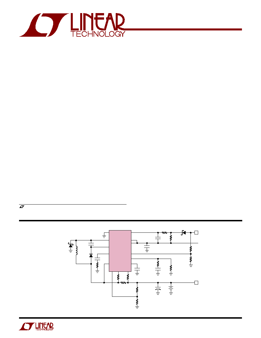
The LT
®
1769 current mode PWM battery charger is a
simple, efficient solution to fast charge modern recharge-
able batteries including lithium-ion (Li-Ion), nickel-metal-
hydride (NiMH) and nickel-cadmium (NiCd) that require
constant-current and/or constant-voltage charging. The
internal switch is capable of delivering 2A** DC current
(3A peak current). Charge current can be programmed by
resistors or a DAC to within 5%. With 0.5% reference voltage
accuracy, the LT1769 meets the critical constant-voltage
charging requirement for Li-Ion cells.
A third control loop is provided to regulate the current
drawn from the input AC adapter. This allows simulta-
neous operation of the equipment and battery charging
without overloading the adapter. Charge current is reduced
to keep the adapter current below specified levels.
The LT1769 can charge batteries ranging from 1V to 20V.
Ground sensing of current is not required and the battery's
negative terminal can be tied directly to ground. A saturat-
ing switch running at 200kHz gives high charging effi-
ciency and small inductor size. A blocking diode is not
required between the chip and the battery because the
chip goes into sleep mode and drains only 3
µ
A when the
wall adapter is unplugged.
Figure 1. 2A Lithium-Ion Battery Charger
s
Chargers for NiCd, NiMH, Lead-Acid, Lithium
Rechargeable Batteries
s
Switching Regulators with Precision Current Limit
, LTC and LT are registered trademarks of Linear Technology Corporation.
*US patent number 5,723,970
**See LT1510 for 1.5A charger; see LT1511 for 3A charger
FEATURES
DESCRIPTIO
U
APPLICATIO S
U
TYPICAL APPLICATIO
U
SW
BOOST
COMP1
CLN
UV
OVP SENSE
BAT
C1
1
µ
F
R
S4
ADAPTER
CURRENT SENSE
R7
500
R5
UNDERVOLTAGE
LOCKOUT
R6
5k
V
IN
(ADAPTER INPUT)
11V TO 28V
V
BAT
C
PROG
1
µ
F
C
IN
*
15
µ
F
300
R
PROG
4.93k
1%
0.33
µ
F
C2
0.47
µ
F
R
S3
200
1%
R
S2
200
1%
L1**
22
µ
H
D2
1N4148
2nF
10k
R
S1
0.05
BATTERY CURRENT
SENSE
R3
390k
0.25%
BATTERY
VOLTAGE SENSE
R4
162k
0.25%
C
OUT
22
µ
F
TANT
8.4V
Li-Ion
LT1769
NOTE: COMPLETE LITHIUM-ION CHARGER,
NO TERMINATION REQUIRED. R
S4
, R7
AND C1 ARE OPTIONAL FOR I
IN
LIMITING
*TOKIN OR UNITED CHEMI-CON/MARCON
CERAMIC SURFACE MOUNT
**22
µ
H SUMIDA CDRH125
SEE APPLICATIONS INFORMATION FOR
INPUT CURRENT LIMIT AND UNDERVOLTAGE LOCKOUT
GENERAL SEMICONDUCTOR. FOR T
J
LESS THEN 100
°
C
MBRS130LT3 CAN BE USED
V
CC
TO MAIN
SYSTEM LOAD
SPIN
D1
SS24
GND
CLP
D3
SS24
1511 · F01
PROG
V
C
+
2
LT1769
1769fa
ABSOLUTE
M
AXI
M
U
M
RATINGS
W
W
W
U
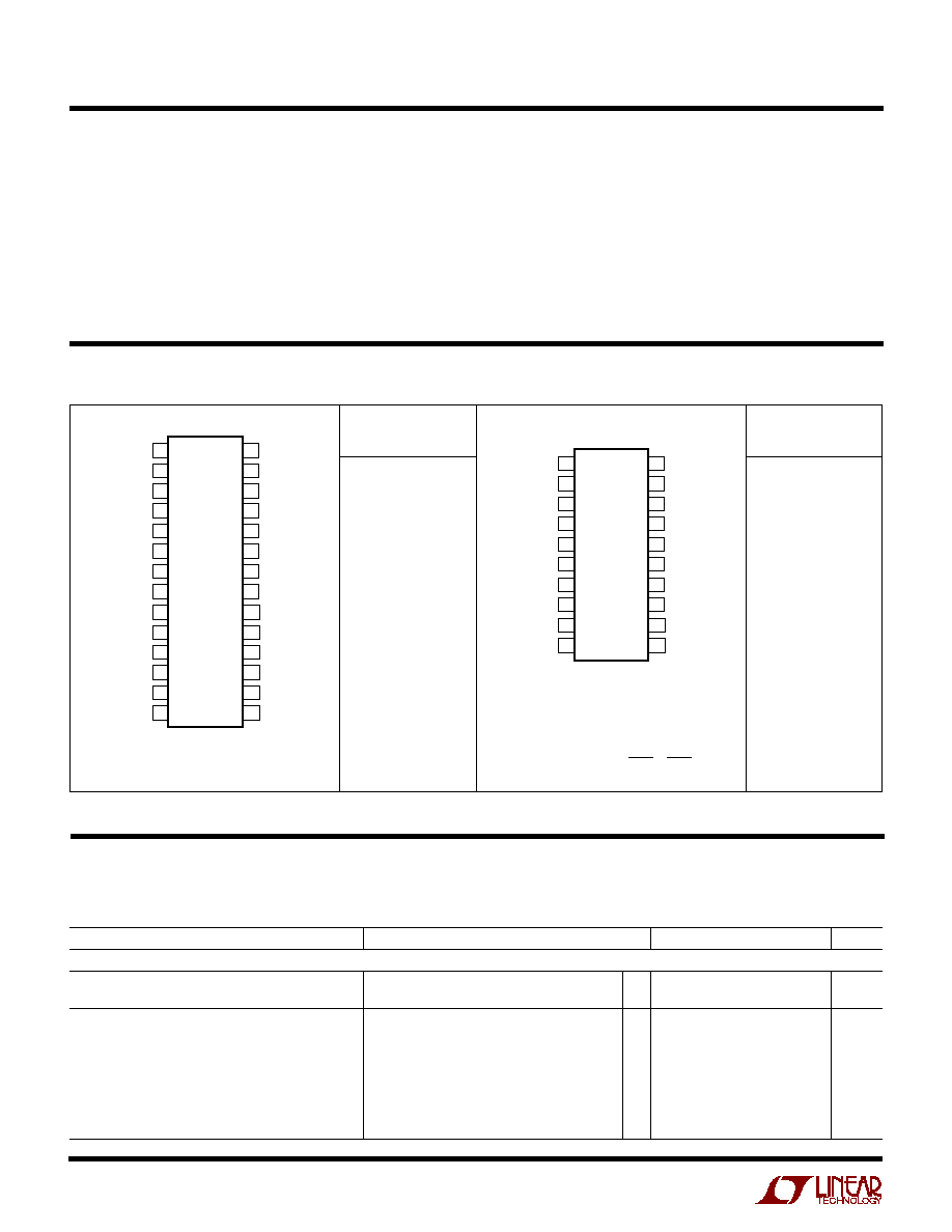
PACKAGE/ORDER I
N
FOR
M
ATIO
N
W
U
U
ORDER PART
NUMBER
*ALL V
CC
PINS SHOULD
BE CONNECTED
TOGETHER CLOSE TO
THE PINS
** ALL GND PINS ARE
FUSED TO INTERNAL DIE
ATTACH PADDLE FOR
HEAT SINKING. CONNECT
THESE PINS TO
EXPANDED PC LANDS
FOR PROPER HEAT
SINKING. 35
°
C/W
THERMAL RESISTANCE
ASSUMES AN INTERNAL
GROUND PLANE
DOUBLING AS A HEAT
SPREADER
LT1769CGN
LT1769IGN
T
JMAX
= 125
°
C,
JA
= 35
°
C/ W**
1
2
3
4
5
6
7
8
9
10
11
12
13
14
TOP VIEW
GN PACKAGE
28-LEAD PLASTIC SSOP
28
27
26
25
24
23
22
21
20
19
18
17
16
15
GND**
GND**
GND**
SW
BOOST
UV
GND**
GND**
OVP
CLP
CLN
COMP1
SENSE
GND**
GND**
GND**
GND**
V
CC1
*
V
CC2
*
V
CC3
*
GND**
PROG
V
C
UV
OUT
COMP2
BAT
SPIN
GND**
Supply Voltage
(V
CC
, CLP and CLN Pin Voltage) ......................... 30V
BOOST Pin Voltage with Respect to V
CC
................. 25V
I
BAT
(Average) ........................................................... 2A
Operating Junction Temperature Range
Commercial ........................................... 0
°
C to 125
°
C
Industrial ......................................... 40
°
C to 125
°
C
Consult LTC Marketing for parts specified with wider operating temperature ranges.
(Note 1)
Operating Ambient Temperature
Commercial ............................................ 0
°
C to 70
°
C
Industrial ........................................... 40
°
C to 85
°
C
Storage Temperature Range ................. 65
°
C to 150
°
C
Lead Temperature (Soldering, 10 sec).................. 300
°
C
ORDER PART
NUMBER
LT1769CFE
LT1769IFE
FE PACKAGE
20-LEAD PLASTIC TSSOP
1
2
3
4
5
6
7
8
9
10
TOP VIEW
20
19
18
17
16
15
14
13
12
11
SW
BOOST
UV
GND
GND
OVP
CLN
CLP
COMP1
SENSE
GND
V
CC1
V
CC2
V
CC3
PROG
V
C
GND
UV
OUT
BAT
SPIN
T
JMAX
= 125
°
C,
JA
= 35
°
C/ W
THE BOTTOM METAL
PLATE OF THIS PACKAGE
IS FUSED TO INTERNAL
GROUND AND IS FOR
HEAT SINKING. SOLDER
THE BOTTOM METAL
PLATE ONTO PCB
GROUND PLANE FOR
HEAT SINKING.
ELECTRICAL CHARACTERISTICS
The
q
denotes specifications which apply over the full operating
temperature range, otherwise specifications are at T
A
= 25
°
C. V
CC
= 16V, V
BAT
= 8V, R
S2
= R
S3
= 200
(see Block Diagram),
V
CLN
= V
CC
. No load on any outputs unless otherwise noted.
PARAMETER
CONDITIONS
MIN
TYP
MAX
UNITS
Overall
Supply Current
V
PROG
= 2.7V, V
CC
20V
q
4.5
6.8
mA
V
PROG
= 2.7V, 20V < V
CC
25V
q
4.6
7.0
mA
Sense Amplifier CA1 Gain and Input Offset Voltage
8V
V
CC
25V , 0V
V
BAT
20V
(With R
S2
= 200
, R
S3
= 200
)
R
PROG
= 4.93k
q
93
100
107
mV
(Measured across R
S1
)(Note 2)
R
PROG
= 49.3k
q
8
10
12
mV
T
A
< 0
°
C
7
13
mV
V
CC
= 28V, V
BAT
= 20V
R
PROG
= 4.93k
q
90
110
mV
R
PROG
= 49.3k
q
7
13
mV
T
A
< 0
°
C
6
14
mV
EXPOSED PAD IS GROUND
(MUST BE SOLDERED TO PCB)
EXPOSED PAD SIZE:
3.0
(.188)
×
4.1
(.162)
3
LT1769
1769fa
ELECTRICAL CHARACTERISTICS
The
q
denotes specifications which apply over the full operating
temperature range, otherwise specifications are at T
A
= 25
°
C. V
CC
= 16V, V
BAT
= 8V, R
S2
= R
S3
= 200
(see Block Diagram),
V
CLN
= V
CC
. No load on any outputs unless otherwise noted.
PARAMETER
CONDITIONS
MIN
TYP
MAX
UNITS
Overall
V
CC
Undervoltage Lockout (Switch OFF) Threshold
Measured at UV Pin
q
6
7
8
V
UV Pin Input Current
0.2V
V
UV
8V
q
0.1
5
µ
A
UV Output Voltage at UV
OUT
Pin
In Undervoltage State, I
UVOUT
= 70
µ
A
q
0.1
0.5
V
UV Output Leakage Current at UV
OUT
Pin
8V
V
UV
, V
UVOUT
= 5V
q
0.1
3
µ
A
Reverse Current from Battery (When V
CC
Is
V
BAT
20V, V
UV
0.4V
3
15
µ
A
Not Connected, V
SW
Is Floating)
Boost Pin Current
V
CC
= 20V, V
BOOST
= 0V
0.1
10
µ
A
V
CC
= 28V, V
BOOST
= 0V
0.25
20
µ
A
2V
V
BOOST
V
CC
< 8V (Switch ON)
6
9
mA
8V
V
BOOST
V
CC
25V (Switch ON)
8
12
mA
Switch
Switch ON Resistance
8V
V
CC
V
MAX
, I
SW
= 2A,
V
BOOST
V
SW
2V
q
0.15
0.25
I
BOOST
/
I
SW
During Switch ON
V
BOOST
= 24V, I
SW
2A
25
35
mA/A
Switch OFF Leakage Current
V
SW
= 0V, V
CC
20V
q
2
100
µ
A
20V < V
CC
28V
q
4
200
µ
A
Minimum I
PROG
for Switch ON
2
4
20
µ
A
Minimum I
PROG
for Switch OFF
q
1
2.4
mA
Maximum V
BAT
for Switch ON
q
V
CC
2
V
Current Sense Amplifier CA1 Inputs (Sense, BAT)
Input Bias Current
q
50
125
µ
A
Input Common Mode Low
q
0.25
V
Input Common Mode High
q
V
CC
2
V
SPIN Input Current
100
200
µ
A
Reference
Reference Voltage (Note 3)
R
PROG
= 4.93k, Measured at OVP with
VA Supplying I
PROG
and Switch OFF
2.448
2.465
2.477
V
Reference Voltage
All Conditions of V
CC
, T
A
0
°
C
q
2.441
2.489
V
T
A
< 0
°
C (Note 4)
q
2.43
2.489
V
Oscillator
Switching Frequency
180
200
220
kHz
Switching Frequency
All Conditions of V
CC
, T
A
0
°
C
q
170
200
230
kHz
T
A
< 0
°
C
q
160
230
kHz
Maximum Duty Cycle
90
93
%
q
85
%
Current Amplifier CA2
Transconductance
V
C
= 1V, I
VC
=
±
1
µ
A
150
250
550
µ
mho
Maximum V
C
for Switch OFF
q
0.6
V
I
VC
Current (Out of Pin)
V
C
0.6V
100
µ
A
V
C
< 0.45V
3
mA
4
LT1769
1769fa
ELECTRICAL CHARACTERISTICS
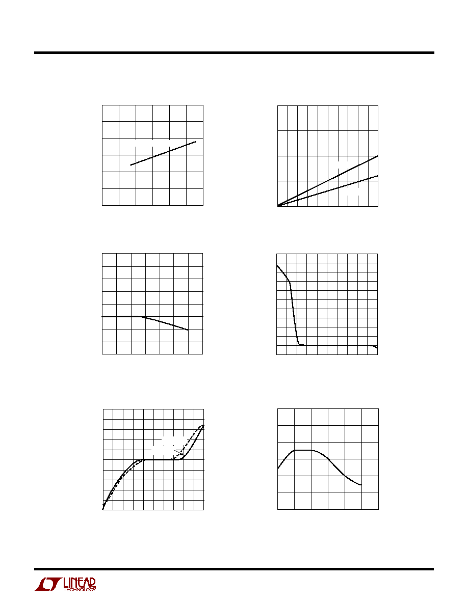
TYPICAL PERFOR
M
A
N
CE CHARACTERISTICS
U
W
Efficiency of Figure 1 Circuit
I
BAT
(A)
0.2
EFFICIENCY (%)
100
98
96
94
92
90
88
86
84
82
80
1.0
1.8
2.2
1769 G01
0.6
1.4
V
IN
= 16.5
V
BAT
= 8.4V
CHARGER EFFICIENCY
INCLUDES LOSS
IN DIODE D3
V
CC
(V)
0
I
CC
(mA)
7.0
6.5
6.0
5.5
5.0
4.5
5
10
15
20
1769 G03
25
30
T
J
= 125
°
C
T
J
= 25
°
C
T
J
= 0
°
C
MAXIMUM DUTY CYCLE
I
CC
vs Duty Cycle
DUTY CYCLE (%)
0
10
30
50
70
I
CC
(mA)
80
1769 G02
20
40
60
8
7
6
5
4
3
2
1
0
T
J
= 125
°
C
T
J
= 0
°
C
T
J
= 25
°
C
V
CC
= 16V
I
CC
vs V
CC
The
q
denotes specifications which apply over the full operating
temperature range, otherwise specifications are at T
A
= 25
°
C. V
CC
= 16V, V
BAT
= 8V. No load on any outputs unless otherwise noted.
Note 1: Absolute Maximum Ratings are those values beyond which the life
of a device may be impaired.
Note 2: Tested with Test Circuit 1.
Note 3: Tested with Test Circuit 2.
Note 4: A linear interpolation can be used for reference voltage
specification between 0
°
C and 40
°
C.
PARAMETER
CONDITIONS
MIN
TYP
MAX
UNITS
Voltage Amplifier VA
Transconductance (Note 3)
Output Current from 50
µ
A to 500
µ
A
0.25
0.6
1.3
mho
Output Source Current
V
OVP
= V
REF
+ 10mV, V
PROG
= V
REF
+ 10mV
1.1
mA
OVP Input Bias Current
VA Output Current at 0.5mA
q
±
3
±
10
nA
VA Output Current at 0.5mA, T
A
> 90
°
C
q
15
25
nA
VA Output Current at 0.5mA, T
A
< 0
°
C
±
15
nA
Current Limit Amplifier CL1, 8V
Input Common Mode
Turn-On Threshold
0.5mA Output Current
93
100
110
mV
Transconductance
Output Current from 50
µ
A to 500
µ
A
0.5
1
2
mho
CLP Input Current
0.5mA Output Current, V
UV
0.4V
0.3
1
µ
A
CLN Input Current
0.5mA Output Current V
UV
0.4V
0.8
2
mA
5
LT1769
1769fa
TYPICAL PERFOR
M
A
N
CE CHARACTERISTICS
U
W
V
CC
(V)
0
V
REF
(V)
0.003
0.002
0.001
0
0.001
0.002
0.003
5
10
15
20
1769 G04
25
30
ALL TEMPERATURES
V
REF
Line Regulation
I
VA
vs
V
OVP
(Voltage Amplifier)
I
VA
(mA)
0
V
OVP
(mV)
4
3
2
1
0
0.8
1769 G05
0.2
0.1
0.3
0.5
0.7
0.9
0.4
0.6
1.0
T
J
= 125
°
C
T
J
= 25
°
C
V
C
Pin Characteristics
V
C
(V)
0
0.2
0.6
1.0
1.4
1.8
I
VC
(mA)
1.20
1.08
0.96
0.84
0.72
0.60
0.48
0.36
0.24
0.12
0
0.12
1.6
1769 G07
0.4
0.8
1.2
2.0
JUNCTION TEMPERATURE (
°
C)
0
DUTY CYCLE (%)
120
1769 G06
40
80
98
97
96
95
94
93
92
91
90
20
60
100
140
Maximum Duty Cycle
Reference Voltage
vs Temperature
JUNCTION TEMPERATURE
0
REFERENCE VOLTAGE (V)
2.470
2.468
2.466
2.464
2.462
2.460
2.458
25
50
75
100
1769 G09
125
150
V
PROG
(V)
0
1
2
3
5
4
I
PROG
(mA)
6
0
6
1769 G08
T
J
= 125
°
C
T
J
= 25
°
C
PROG Pin Characteristics