 | ÐлекÑÑоннÑй компоненÑ: LT1792IS8 | СкаÑаÑÑ:  PDF PDF  ZIP ZIP |
Äîêóìåíòàöèÿ è îïèñàíèÿ www.docs.chipfind.ru
1
LT1792
Low Noise, Precision,
JFET Input Op Amp
The LT
®
1792 achieves a new standard of excellence in
noise performance for a JFET op amp. The 4.2nV/
Hz
voltage noise combined with low current noise and
picoampere bias currents make the LT1792 an ideal choice
for amplifying low level signals from high impedance
capacitive transducers.
The LT1792 is unconditionally stable for gains of 1 or more,
even with load capacitances up to 1000pF. Other key
features are 600
µ
V V
OS
and a voltage gain of over 4 million.
Each individual amplifier is 100% tested for voltage noise,
slew rate and gain bandwidth.
The design of the LT1792 has been optimized to achieve
true precision performance with an industry standard
pinout in the SO-8 package. Specifications are also pro-
vided for
±
5V supplies.
s
100% Tested Low Voltage Noise: 6nV/
Hz Max
s
A Grade 100% Temperature Tested
s
Voltage Gain: 1.2 Million Min
s
Offset Voltage Over Temp: 800
µ
V Max
s
Gain-Bandwidth Product: 5.6MHz Typ
s
Guaranteed Specifications with
±
5V Supplies
, LTC and LT are registered trademarks of Linear Technology Corporation.
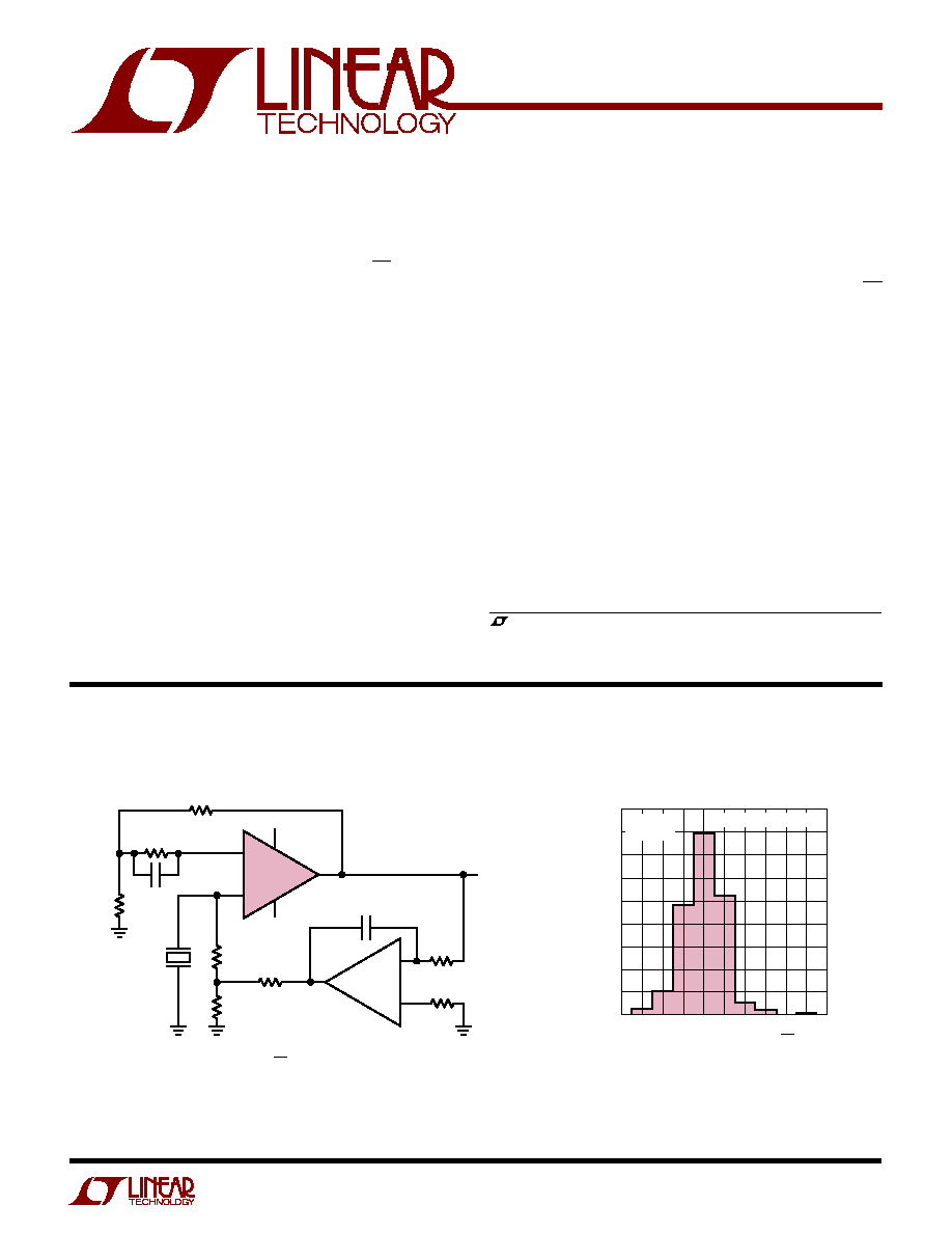
Low Noise Hydrophone Amplifier with DC Servo
+
+
7
4
5V TO 15V
6
2
3
5V TO 15V
C2
0.47
µ
F
2
3
6
R8
100M
R6
100k
R4
1M
R5
1M
LT1792
LT1097
R3
3.9k
C1*
R1*
100M
R7
1M
R2
200
C
T
HYDRO-
PHONE
OUTPUT
DC OUTPUT
2.5mV FOR T
A
< 70
°
C
OUTPUT VOLTAGE NOISE = 128nV/
Hz AT 1kHz (GAIN = 20)
C1
C
T
100pF TO 5000pF; R4C2 > R8C
T
; *OPTIONAL
1792 TA01
INPUT VOLTAGE NOISE (nV/
Hz)
3.6
PERCENT OF UNITS (%)
40
30
20
10
0
4.0
4.4 4.6
5.6
1792 TA02
3.8
4.2
4.8 5.0 5.2 5.4
V
S
=
±
15V
T
A
= 25
°
C
270 OP AMPS TESTED
1kHz Input Noise Voltage Distribution
s
Photocurrent Amplifiers
s
Hydrophone Amplifiers
s
High Sensitivity Piezoelectric Accelerometers
s
Low Voltage and Current Noise Instrumentation
Amplifier Front Ends
s
Two and Three Op Amp Instrumentation Amplifiers
s
Active Filters
FEATURES
DESCRIPTIO
U
APPLICATIO S
U
TYPICAL APPLICATIO
U

2
LT1792
A
U
G
W
A
W
U
W
A
R
BSOLUTE
XI
TI
S
(Note 1)
Supply Voltage .....................................................
±
20V
Differential Input Voltage ......................................
±
40V
Input Voltage (Equal to Supply Voltage) ...............
±
20V
Output Short-Circuit Duration ........................ Indefinite
Operating Temperature Range ............... 40
°
C to 85
°
C
Specified Temperature Range
Commercial (Note 8) ......................... 40
°
C to 85
°
C
Industrial ........................................... 40
°
C to 85
°
C
Storage Temperature Range ................ 65
°
C to 150
°
C
Lead Temperature (Soldering, 10 sec) ................ 300
°
C
1792AI
1792I
ORDER PART
NUMBER
T
JMAX
= 160
°
C,
JA
= 190
°
C/W
T
JMAX
= 140
°
C,
JA
= 130
°
C/W
1
2
3
4
8
7
6
5
TOP VIEW
N8 PACKAGE
8-LEAD PDIP
A
V
OS
ADJ
IN A
+IN A
V
NC
V
+
OUT
V
OS
ADJ
1
2
3
4
8
7
6
5
TOP VIEW
S8 PACKAGE
8-LEAD PLASTIC SO
V
OS
ADJ
IN A
+IN A
V
NC
V+
OUT
V
OS
ADJ
A
ORDER PART
NUMBER
S8 PART MARKING
Consult factory for Military grade parts.
W
U
U
PACKAGE/ORDER I FOR ATIO
LT1792ACN8
LT1792CN8
LT1792AIN8
LT1792IN8
LT1792ACS8
LT1792CS8
LT1792AIS8
LT1792IS8
ELECTRICAL C
C
HARA TERISTICS
T
A
= 25
°
C, V
S
=
±
15V, V
CM
= 0V, unless otherwise noted. (Note 9)
LT1792C/LT1792I
SYMBOL
PARAMETER
CONDITIONS (Note 2)
MIN
TYP
MAX
MIN
TYP
MAX
UNITS
V
OS
Input Offset Voltage
0.2
0.6
0.2
0.8
mV
V
S
=
±
5V
0.4
1.0
0.4
1.3
mV
I
OS
Input Offset Current
Warmed Up (Note 3)
100
400
100
400
pA
I
B
Input Bias Current
Warmed Up (Note 3)
300
800
300
800
pA
e
n
Input Noise Voltage
0.1Hz to 10Hz
2.4
2.4
µ
V
P-P
Input Noise Voltage Density
f
O
= 10Hz
8.3
8.3
nV/
Hz
f
O
= 1000Hz
4.2
6.0
4.2
6.0
nV/
Hz
i
n
Input Noise Current Density
f
O
= 10Hz, f
O
= 1000Hz (Note 4)
10
10
fA/
Hz
R
IN
Input Resistance
Differential Mode
10
11
10
11
Common Mode
V
CM
= 10V to 8V
10
11
10
11
V
CM
= 8V to 11V
10
10
10
10
C
IN
Input Capacitance
14
14
pF
V
S
=
±
5V
27
27
pF
V
CM
Input Voltage Range (Note 5)
13.0
13.5
13.0
13.5
V
10.5
11.0
10.5
11.0
V
CMRR
Common Mode Rejection Ratio
V
CM
= 10V to 13V
85
105
82
100
dB
PSRR
Power Supply Rejection Ratio
V
S
=
±
4.5V to
±
20V
88
105
83
98
dB
1792A
1792
LT1792AC/LT1792AI

3
LT1792
ELECTRICAL C
C
HARA TERISTICS
T
A
= 25
°
C, V
S
=
±
15V, V
CM
= 0V, unless otherwise noted.
LT1792C/LT1792I
SYMBOL
PARAMETER
CONDITIONS
MIN
TYP
MAX
MIN
TYP
MAX
UNITS
A
VOL
Large-Signal Voltage Gain
V
O
=
±
12V, R
L
= 10k
1200
4800
1000
4500
V/mV
V
O
=
±
10V, R
L
= 1k
600
4000
500
3000
V/mV
V
OUT
Output Voltage Swing
R
L
= 10k
±
13.0
±
13.2
±
13.0
±
13.2
V
R
L
= 1k
±
12.0
±
12.3
±
12.0
±
12.3
V
SR
Slew Rate
R
L
2k (Note 7)
2.3
3.4
2.3
3.4
V/
µ
s
GBW
Gain-Bandwidth Product
f
O
= 100kHz
4.0
5.6
4.0
5.6
MHz
I
S
Supply Current
4.2
5.20
4.2
5.20
mA
V
S
=
±
5V
4.2
5.15
4.2
5.15
mA
Offset Voltage
R
POT
(to V
EE
) = 10k
10
10
mV
Adjustment Range
The
q
denotes specifications which apply over the temperature range 0
°
C
T
A
70
°
C. V
S
=
±
15V, V
CM
= 0V,
unless otherwise noted. (Note 9)
LT1792AC
LT1792C
SYMBOL
PARAMETER
CONDITIONS (Note 2)
MIN
TYP
MAX
MIN
TYP
MAX
UNITS
V
OS
Input Offset Voltage
q
0.4
0.8
0.8
2.7
mV
V
S
=
±
5V
q
0.6
1.2
1.2
3.2
mV
V
OS
Average Input Offset
(Note 6)
q
4
10
7
40
µ
V/
°
C
Temp
Voltage Drift
I
OS
Input Offset Current
q
180
500
180
500
pA
I
B
Input Bias Current
q
500
1800
500
1800
pA
V
CM
Input Voltage Range
q
12.9
13.4
12.9
13.4
V
q
10.0
10.8
10.0
10.8
V
CMRR
Common Mode Rejection Ratio
V
CM
= 10V to 12.9V
q
81
104
79
99
dB
PSRR
Power Supply Rejection Ratio
V
S
=
±
4.5V to
±
20V
q
85
99
81
97
dB
A
VOL
Large-Signal Voltage Gain
V
O
=
±
12V, R
L
= 10k
q
900
3600
800
3400
V/mV
V
O
=
±
10V, R
L
= 1k
q
500
2600
400
2400
V/mV
V
OUT
Output Voltage Swing
R
L
= 10k
q
±
12.9
±
13.2
±
12.9
±
13.2
V
R
L
= 1k
q
±
11.9
±
12.15
±
11.9
±
12.15
V
SR
Slew Rate
R
L
2k
(Note 7)
q
2.1
3.1
2.1
3.1
V/
µ
s
GBW
Gain-Bandwidth Product
f
O
= 100kHz
q
3.2
4.5
3.2
4.5
MHz
I
S
Supply Current
q
4.2
5.30
4.2
5.30
mA
V
S
=
±
5V
q
4.2
5.25
4.2
5.25
mA
LT1792AC/LT1792AI

4
LT1792
ELECTRICAL C
C
HARA TERISTICS
The
q
denotes specifications which apply over the temperature range
40
°
C
T
A
85
°
C. V
S
=
±
15V, V
CM
= 0V, unless otherwise noted. (Notes 8, 9)
SYMBOL
PARAMETER
CONDITIONS (Note 2)
MIN
TYP
MAX
MIN
TYP
MAX
UNITS
V
OS
Input Offset Voltage
q
0.5
1.0
1.2
3.7
mV
V
S
=
±
5V
q
0.8
1.4
1.5
4.2
mV
V
OS
Average Input Offset
(Note 6)
q
4
10
7
40
µ
V/
°
C
Temp
Voltage Drift
I
OS
Input Offset Current
q
300
800
300
800
pA
I
B
Input Bias Current
q
1200
4000
1200
4000
pA
V
CM
Input Voltage Range
q
12.6
13.0
12.6
13.0
V
q
10.0
10.5
10.0
10.5
V
CMRR
Common Mode Rejection Ratio
V
CM
= 10V to 12.6V
q
80
103
78
98
dB
PSRR
Power Supply Rejection Ratio
V
S
=
±
4.5V to
±
20V
q
83
98
79
96
dB
A
VOL
Large-Signal Voltage Gain
V
O
=
±
12V, R
L
= 10k
q
850
3300
750
3000
V/mV
V
O
=
±
10V, R
L
= 1k
q
400
2200
300
2000
V/mV
V
OUT
Output Voltage Swing
R
L
= 10k
q
±
12.8
±
13.1
±
12.8
±
13.1
V
R
L
= 1k
q
±
11.8
±
12.1
±
11.8
±
12.1
V
SR
Slew Rate
R
L
2k
q
2.0
3.0
2.0
3.0
V/
µ
s
GBW
Gain-Bandwidth Product
f
O
= 100kHz
q
2.9
4.3
2.9
4.3
MHz
I
S
Supply Current
q
4.2
5.40
4.2
5.40
mA
V
S
=
±
5V
q
4.2
5.35
4.2
5.35
mA
Note 6: This parameter is not 100% tested.
Note 7: Slew rate is measured in A
V
= 1; input signal is
±
7.5V, output
measured at
±
2.5V.
Note 8: The LT1792AC and LT1792C are guaranteed to meet specified
performance from 0
°
C to 70
°
C and are designed, characterized and
expected to meet these extended temperature limits, but are not tested at
40
°
C and 85
°
C. The LT1792I is guaranteed to meet the extended
temperature limits. The LT1792AC and LT1792AI grade are 100%
temperature tested for the specified temperature range.
Note 9: The LT1792 is measured in an automated tester in less than one
second after application of power. Depending on the package used,
power dissipation, heat sinking, and air flow conditions, the fully
warmed-up chip temperature can be 10
°
C to 50
°
C higher than the
ambient temperature.
Note 1: Absolute Maximum Ratings are those values beyond which the
life of a device may be impaired.
Note 2: Typical parameters are defined as the 60% yield of parameter
distributions of individual amplifiers.
Note 3: Warmed-up I
B
and I
OS
readings are extrapolated to a chip
temperature of 32
°
C from 25
°
C measurements and 32
°
C characterization
data.
Note 4: Current noise is calculated from the formula:
i
n
= (2qI
B
)
1/2
where q = 1.6 · 10
19
coulomb. The noise of source resistors up to 200M
swamps the contribution of current noise.
Note 5: Input voltage range functionality is assured by testing offset
voltage at the input voltage range limits to a maximum of 2.3mV
(A grade), to 2.8mV (C grade).
LT1792AC/LT1792AI
LT1792C/LT1792I

5
LT1792
C
C
HARA TERISTICS
U
W
A
TYPICAL PERFOR
CE
TIME (SEC)
0
VOLTAGE NOISE (1
µ
V/DIV)
8
1792 G01
2
4
6
10
0.1Hz to 10Hz Voltage Noise
TEMPERATURE (
°
C)
75
0
1
3
4
5
10
7
25
25
50
1792 G03
2
8
9
6
50
0
75
100
125
VOLTAGE NOISE (AT 1kHz) (nV/
Hz)
V
S
=
±
15V
Voltage Noise
vs Chip Temperature
Voltage Gain vs Frequency
FREQUENCY (Hz)
0.01
VOLTAGE GAIN (dB)
100
140
180
1M
1792 G08
60
20
80
120
160
40
0
20
1
100
10k
100M
Common Mode Limit
vs Temperature
TEMPERATURE (
°
C)
60
COMMON MODE LIMIT
REFERRED TO POWER SUPPLY (V)
2.0
1.0
V
+
0
100
1792 G05
4.0
3.0
1.5
0.5
3.5
2.5
V
+ 2.0
20
20
60
140
V
+
= 5V TO 20V
V
= 5V TO 20V
Input Bias and Offset Current
Over the Common Mode Range
COMMON-MODE RANGE (V)
15
INPUT BIAS AND OFFSET CURRENTS (pA)
400
300
200
100
0
10
5
0
5
1792 G22
10
15
T
A
= 25
°
C
V
S
=
±
15V
NOT WARMED UP
OFFSET CURRENT
BIAS CURRENT
Common Mode Rejection Ratio
vs Frequency
FREQUENCY (Hz)
40
COMMON MODE REJECTION RATIO (dB)
80
120
20
60
100
1k
100k
1M
10M
1792 G06
0
10k
T
A
= 25
°
C
V
S
=
±
15V
FREQUENCY (Hz)
1
10
1
10
100
100
10k
1k
1792 G02
RMS VOLTAGE NOISE DENSITY (nV/
Hz)
V
S
=
±
15V
T
A
= 25
°
C
1/f CORNER
30Hz
Voltage Noise vs Frequency
Input Bias and Offset Current
vs Chip Temperature
TEMPERATURE (
°
C)
75
INPUT BIAS AND OFFSET CURRENT (nA)
1
I
B
I
OS
10
125
1792 G04
0.1
0.3
3
0.03
0.01
25
25
75
50
0
50
100
100
30
V
S
=
±
15V
FREQUENCY (Hz)
10
POWER SUPPLY REJECTION RATIO (dB)
120
100
80
60
40
20
0
100
1k
10k
100k
1792 G07
1M
10M
T
A
= 25
°
C
+PSRR
PSRR
Power Supply Rejection Ratio
vs Frequency