 | ÐлекÑÑоннÑй компоненÑ: LT1793IS8 | СкаÑаÑÑ:  PDF PDF  ZIP ZIP |
Äîêóìåíòàöèÿ è îïèñàíèÿ www.docs.chipfind.ru
1
LT1793
Low Noise,
Picoampere Bias Current,
JFET Input Op Amp
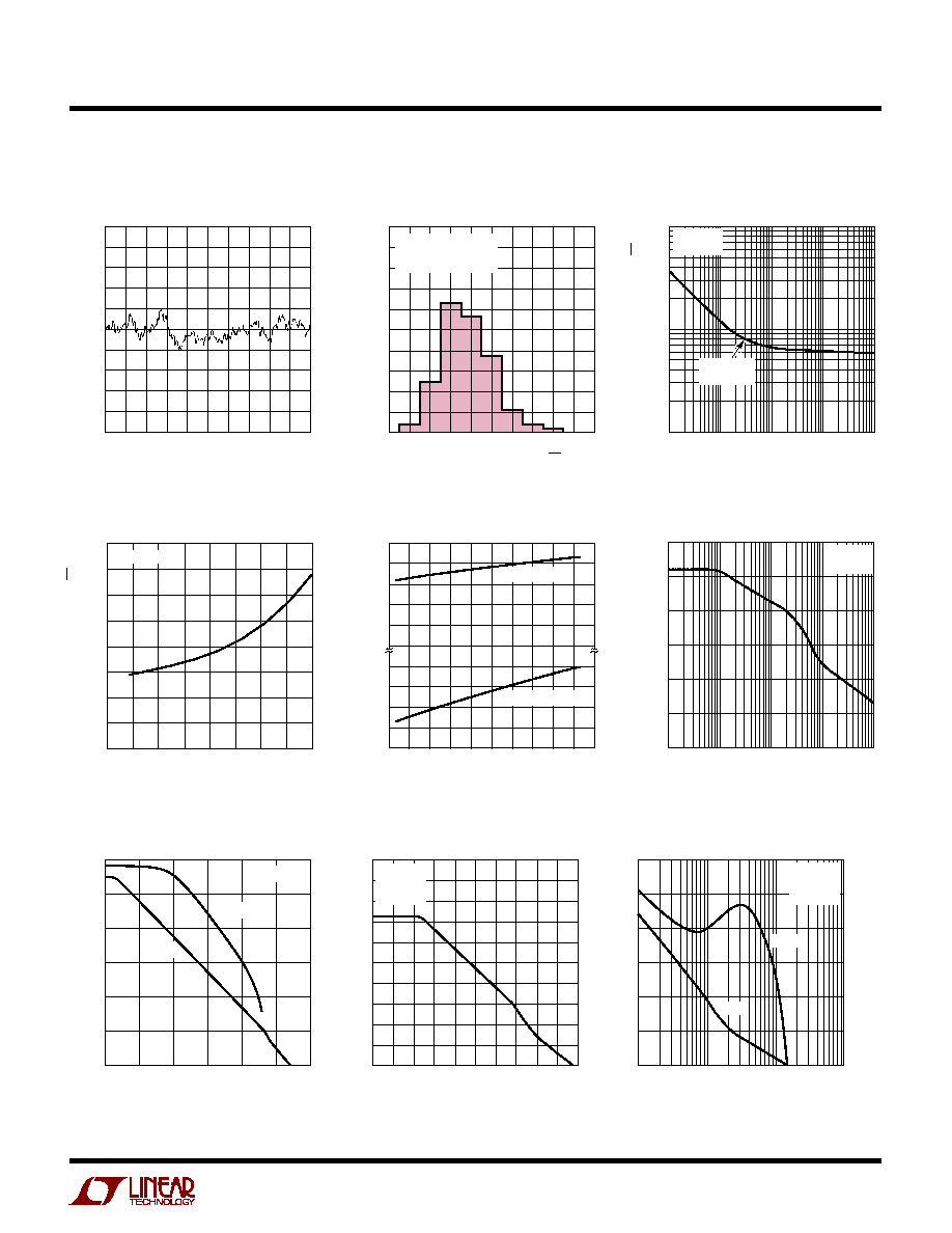
1kHz Output Voltage Noise
Density vs Source Resistance
SOURCE RESISTANCE (
)
10k
1k
100
10
1
100
10k
100k
1M
1k
10M
1793 TA02
TOTAL 1kHz VOLTAGE NOISE DENSITY (nV/
Hz)
100M 1G
+
V
N
R
SOURCE
T
A
= 25
°
C
V
S
=
±
15V
V
N
SOURCE
RESISTANCE
ONLY
V
N
=
(V
OP AMP
)
2
+ 4kTR
S
+ 2qI
B
R
S
2
The LT
®
1793 achieves a new standard of excellence in
noise performance for a JFET op amp. For the first time low
voltage noise (6nV/
Hz) is simultaneously offered with
extremely low current noise (0.8fA/
Hz), providing the
lowest total noise for high impedance transducer applica-
tions. Unlike most JFET op amps, the very low input bias
current (3pA typ) is maintained over the entire common
mode range which results in an extremely high input resis-
tance (10
13
). When combined with a very low input ca-
pacitance (1.5pF) an extremely high input impedance
results, making the LT1793 the first choice for amplifying
low level signals from high impedance transducers. The
low input capacitance also assures high gain linearity when
buffering AC signals from high impedance transducers.
The LT1793 is unconditionally stable for gains of 1 or more,
even with 1000pF capacitive loads. Other key features are
250
µ
V V
OS
and a voltage gain over 4 million. Each indi-
vidual amplifier is 100% tested for voltage noise, slew rate
(3.4V/
µ
s) and gain-bandwidth product (4.2MHz).
Specifications at
±
5V supply operation are also provided.
For an even lower voltage noise please see the LT1792 data
sheet.
s
Input Bias Current, Warmed Up: 10pA Max
s
100% Tested Low Voltage Noise: 8nV/
Hz Max
s
A Grade 100% Temperature Tested
s
Offset Voltage Over Temp: 1mV Max
s
Input Resistance: 10
13
s
Very Low Input Capacitance: 1.5pF
s
Voltage Gain: 1 Million Min
s
Gain-Bandwidth Product: 4.2MHz Typ
s
Guaranteed Specifications with
±
5V Supplies
s
Photocurrent Amplifiers
s
Hydrophone Amplifiers
s
High Sensitivity Piezoelectric Accelerometers
s
Low Voltage and Current Noise Instrumentation
Amplifier Front Ends
s
Two and Three Op Amp Instrumentation Amplifiers
s
Active Filters
, LTC and LT are registered trademarks of Linear Technology Corporation.
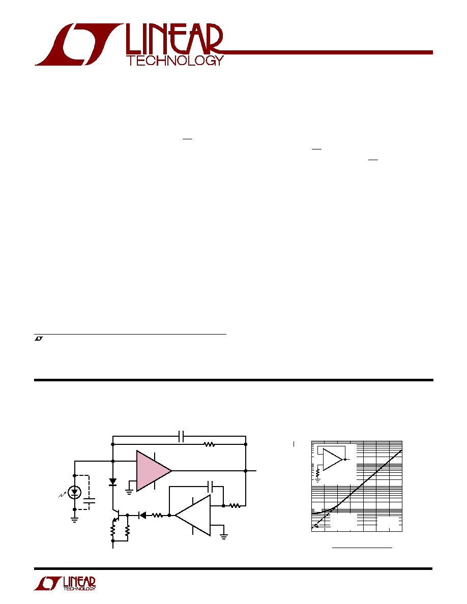
1793 TA01
R1
1M
C1
2pF
+
LT1097
R2C2 > C1R1
C
D
= PARASITIC PHOTODIODE CAPACITANCE
V
OUT
= 100mV/
µ
WATT FOR 200nm WAVE LENGTH
330mV/
µ
WATT FOR 633nm WAVE LENGTH
R5
10k
D2
1N914
V
V
V
+
R4
1k
D1
1N914
R3
1k
6
7
4
3
2
+
LT1793
V
+
V
C2 0.022
µ
F
HAMAMATSU
S1336-5BK
(908) 231-0960
V
OUT
R2
100k
C
D
2N3904
Low Noise Light Sensor with DC Servo
FEATURES
DESCRIPTIO
U
APPLICATIO S
U
TYPICAL APPLICATIO
U
2
LT1793
A
U
G
W
A
W
U
W
A
R
BSOLUTE
XI
TI
S
(Note 1)
Supply Voltage .....................................................
±
20V
Differential Input Voltage ......................................
±
40V
Input Voltage (Equal to Supply Voltage) ...............
±
20V
Output Short-Circuit Duration ........................ Indefinite
Operating Temperature Range ............... 40
°
C to 85
°
C
Specified Temperature Range
Commercial (Note 8) ......................... 40
°
C to 85
°
C
Industrial ........................................... 40
°
C to 85
°
C
Storage Temperature Range ................ 65
°
C to 150
°
C
Lead Temperature (Soldering, 10 sec) ................ 300
°
C
W
U
U
PACKAGE/ORDER I FOR ATIO
Consult factory for Military grade parts.
T
JMAX
= 150
°
C,
JA
= 80
°
C/W
ORDER PART
NUMBER
LT1793ACN8
LT1793CN8
LT1793AIN8
LT1793IN8
1
2
3
4
8
7
6
5
TOP VIEW
N8 PACKAGE
8-LEAD PDIP
A
V
OS
ADJ
IN A
+ IN A
V
NC
V
+
OUT
V
OS
ADJ
ORDER PART
NUMBER
S8 PART MARKING
LT1793ACS8
LT1793CS8
LT1793AIS8
LT1793IS8
1793A
1793
T
JMAX
= 160
°
C,
JA
= 190
°
C/W
1
2
3
4
8
7
6
5
TOP VIEW
S8 PACKAGE
8-LEAD PLASTIC SO
V
OS
ADJ
IN A
+IN A
V
NC
V+
OUT
V
OS
ADJ
A
1793AI
1793I
LT1793C/LT1793I
SYMBOL
PARAMETER
CONDITIONS (Note 2)
MIN
TYP
MAX
MIN
TYP
MAX
UNITS
V
OS
Input Offset Voltage
0.25
0.8
0.25
0.9
mV
V
S
=
±
5V
0.45
1.4
0.45
1.6
mV
I
OS
Input Offset Current
Warmed Up (Note 3)
1.5
7
2.5
15
pA
T
J
= 25
°
C (Note 6)
0.5
2
0.7
4
pA
I
B
Input Bias Current
Warmed Up (Note 3)
3
10
4.0
20
pA
T
J
= 25
°
C (Note 6)
1
3
1.5
5
pA
e
n
Input Noise Voltage
0.1Hz to 10Hz
2.4
2.4
µ
V
P-P
Input Noise Voltage Density
f
O
= 10Hz
11.5
11.5
nV/
Hz
f
O
= 1000Hz
6
8
6
8
nV/
Hz
i
n
Input Noise Current Density
f
O
= 10Hz, f
O
= 1kHz (Note 4)
0.8
1
fA/
Hz
R
IN
Input Resistance
Differential Mode
10
14
10
14
Common Mode
V
CM
= 10V to 13V
10
13
10
13
C
IN
Input Capacitance
1.5
1.5
pF
V
S
=
±
5V
2.0
2.0
pF
V
CM
Input Voltage Range (Note 5)
13.0
13.5
13.0
13.5
V
10.5
11.0
10.5
11.0
V
CMRR
Common Mode Rejection Ratio
V
CM
= 10V to 13V
83
102
81
96
dB
PSRR
Power Supply Rejection Ratio
V
S
=
±
4.5V to
±
20V
85
98
83
95
dB
T
A
= 25
°
C, V
S
=
±
15V, V
CM
= 0V, unless otherwise noted.
ELECTRICAL C
C
HARA TERISTICS
LT1793AC/LT1793AI
3
LT1793
ELECTRICAL C
C
HARA TERISTICS
T
A
= 25
°
C, V
S
=
±
15V, V
CM
= 0V, unless otherwise noted.
LT1793C/LT1793I
SYMBOL
PARAMETER
CONDITIONS (Note 2)
MIN
TYP
MAX
MIN
TYP
MAX
UNITS
A
VOL
Large-Signal Voltage Gain
V
O
=
±
12V, R
L
= 10k
1000
4500
900
4400
V/mV
V
O
=
±
10V, R
L
= 1k
500
3500
400
3000
V/mV
V
OUT
Output Voltage Swing
R
L
= 10k
±
13.0
±
13.2
±
13.0
±
13.2
V
R
L
= 1k
±
12.0
±
12.3
±
12.0
±
12.3
V
SR
Slew Rate
R
L
2k (Note 7)
2.3
3.4
2.3
3.4
V/
µ
s
GBW
Gain-Bandwidth Product
f
O
= 100kHz
2.5
4.2
2.5
4.2
MHz
I
S
Supply Current
4.2
5.20
4.2
5.20
mA
V
S
=
±
5V
4.2
5.15
4.2
5.15
mA
Offset Voltage
R
POT
(to V
EE
) = 10k
13
13
mV
Adjustment Range
LT1793AC
LT1793C
SYMBOL
PARAMETER
CONDITIONS (Note 2)
MIN
TYP
MAX
MIN
TYP
MAX
UNITS
V
OS
Input Offset Voltage
q
0.50
1.0
1.0
3.5
mV
V
S
=
±
5V
q
0.75
1.6
1.6
4.2
mV
V
OS
Average Input Offset
(Note 6)
q
5
13
8
50
µ
V/
°
C
Temp
Voltage Drift
I
OS
Input Offset Current
q
15
100
20
130
pA
I
B
Input Bias Current
q
130
400
150
500
pA
V
CM
Input Voltage Range (Note 5)
q
12.9
13.4
12.9
13.4
V
q
10.0
10.8
10.0
10.8
V
CMRR
Common Mode Rejection Ratio
V
CM
= 10V to 12.9V
q
79
100
77
95
dB
PSRR
Power Supply Rejection Ratio
V
S
=
±
4.5V to
±
20V
q
83
97
81
94
dB
A
VOL
Large-Signal Voltage Gain
V
O
=
±
12V, R
L
= 10k
q
900
3600
800
3400
V/mV
V
O
=
±
10V, R
L
= 1k
q
500
2600
400
2400
V/mV
V
OUT
Output Voltage Swing
R
L
= 10k
q
±
12.9
±
13.2
±
12.9
±
13.2
V
R
L
= 1k
q
±
11.9
±
12.15
±
11.9
±
12.15
V
SR
Slew Rate
R
L
2k (Note 7)
q
2.2
3.3
2.2
3.3
V/
µ
s
GBW
Gain-Bandwidth Product
f
O
= 100kHz
q
2.2
3.3
2.2
3.3
MHz
I
S
Supply Current
q
4.2
5.30
4.2
5.30
mA
V
S
=
±
5V
q
4.2
5.25
4.2
5.25
mA
The
q
denotes specifications which apply over the temperature range 0
°
C
T
A
70
°
C, otherwise specifications are at T
A
= 25
°
C.
V
S
=
±
15V, V
CM
= 0V, unless otherwise noted. (Note 9)
LT1793AC/LT1793AI
4
LT1793
ELECTRICAL C
C
HARA TERISTICS
The
q
denotes specifications which apply over the temperature range
40
°
C
T
A
85
°
C. V
S
=
±
15V, V
CM
= 0V, unless otherwise noted. (Notes 8, 9)
SYMBOL
PARAMETER
CONDITIONS (Note 2)
MIN
TYP
MAX
MIN
TYP
MAX
UNITS
V
OS
Input Offset Voltage
q
0.65
1.3
1.6
4.8
mV
V
S
=
±
5V
q
1.00
1.9
2.0
5.5
mV
V
OS
Average Input Offset
(Note 6)
q
5
13
9
50
µ
V/
°
C
Temp
Voltage Drift
I
OS
Input Offset Current
q
80
300
100
400
pA
I
B
Input Bias Current
q
700
2400
800
3000
pA
V
CM
Input Voltage Range (Note 5)
q
12.6
13.0
12.6
13.0
V
q
10.0
10.5
10.0
10.5
V
CMRR
Common Mode Rejection Ratio
V
CM
= 10V to 12.6V
q
78
99
76
94
dB
PSRR
Power Supply Rejection Ratio
V
S
=
±
4.5V to
±
20V
q
81
96
79
93
dB
A
VOL
Large-Signal Voltage Gain
V
O
=
±
12V, R
L
= 10k
q
850
3300
750
3000
V/mV
V
O
=
±
10V, R
L
= 1k
q
400
2200
300
2000
V/mV
V
OUT
Output Voltage Swing
R
L
= 10k
q
±
12.8
±
13.1
±
12.8
±
13.1
V
R
L
= 1k
q
±
11.8
±
12.1
±
11.8
±
12.1
V
SR
Slew Rate
R
L
2k
q
2.1
3.2
2.1
3.2
V/
µ
s
GBW
Gain-Bandwidth Product
f
O
= 100kHz
q
2
3.1
2
3.1
MHz
I
S
Supply Current
q
4.2
5.40
4.2
5.40
mA
V
S
=
±
5V
q
4.2
5.35
4.2
5.35
mA
Note 1: Absolute Maximum Ratings are those values beyond which the life
of a device may be impaired.
Note 2: Typical parameters are defined as the 60% yield of parameter
distributions of individual amplifiers.
Note 3: I
B
and I
OS
readings are extrapolated to a warmed-up temperature
from 25
°
C measurements and 32
°
C characterization data.
Note 4: Current noise is calculated from the formula:
i
n
= (2qI
B
)
1/2
where q = 1.6 · 10
19
coulomb. The noise of source resistors up to 200M
swamps the contribution of current noise.
Note 5: Input voltage range functionality is assured by testing offset
voltage at the input voltage range limits to a maximum of 2.3mV
(A grade) to 2.8mV (C grade).
Note 6: This parameter is not 100% tested.
Note 7: Slew rate is measured in A
V
= 1; input signal is
±
7.5V, output
measured at
±
2.5V.
Note 8: The LT1793AC and LT1793C are guaranteed to meet specified
performance from 0
°
C to 70
°
C and are designed, characterized and
expected to meet these extended temperature limits, but are not tested at
40
°
C and 85
°
C. The LT1793I is guaranteed to meet the extended
temperature limits. The LT1793AC and LT1793AI grade are 100%
temperature tested for the specified temperature range.
Note 9: The LT1793 is measured in an automated tester in less than one
second after application of power. Depending on the package used, power
dissipation, heat sinking, and air flow conditions, the fully warmed-up chip
temperature can be 10
°
C to 50
°
C higher than the ambient temperature.
LT1793AC/LT1793AI
LT1793C/LT1793I
5
LT1793
C
C
HARA TERISTICS
U
W
A
TYPICAL PERFOR
CE
Voltage Noise vs Frequency
INPUT VOLTAGE NOISE (nV/
Hz)
4.2
PERCENT OF UNITS (%)
30
40
50
7.4
1793 G02
20
10
0
5.0
5.8
6.6
4.6
7.8
5.4
6.2
7.0
8.2
T
A
= 25
°
C
V
S
=
±
15V
510 OP AMPS TESTED
1kHz Input Noise Voltage
Distribution
TIME (SEC)
VOLTAGE NOISE (1
µ
V/DIV)
2
4
6
8
1793 G01
10
0
0.1Hz to 10Hz Voltage Noise
FREQUENCY (Hz)
1
10
1
10
100
100
1k
10k
1793 G03
RMS VOLTAGE NOISE DENSITY (nV/
Hz)
T
A
= 25
°
C
V
S
=
±
15V
1/f CORNER
30Hz
Common Mode Limit
vs Temperature
Voltage Noise
vs Chip Temperature
TEMPERATURE (
°
C)
75
VOLTAGE NOISE (AT 1kHz) (nV/
Hz)
6
7
8
1793 G04
5
4
2
0
50
100
3
10
9
50 25
25
75
125
V
S
=
±
15V
TEMPERATURE (
°
C)
60
COMMON MODE LIMIT (V)
REFERRED TO POWER SUPPLY
V
+
0
0.5
1.0
1.5
2.0
100
1793 G05
4.0
3.0
2.5
3.5
V
+2.0
20
20
60
140
V
+
= 5V TO 20V
V
= 5V TO 20V
Common Mode Rejection Ratio
vs Frequency
FREQUENCY (Hz)
40
COMMON MODE REJECTION RATIO (dB)
80
120
20
60
100
1k
100k
1M
10M
1793 G06
0
10k
T
A
= 25
°
C
V
S
=
±
15V
Power Supply Rejection Ratio
vs Frequency
FREQUENCY (Hz)
10
0
POWER SUPPLY REJECTION RATIO (dB)
20
40
60
80
120
100
1k
10k
100k
1793 G07
1M
10M
100
T
A
= 25
°
C
+PSRR
PSRR
Gain and Phase Shift
vs Frequency
FREQUENCY (MHz)
0.1
10
VOLTAGE GAIN (dB)
PHASE SHIFT (DEG)
30
40
50
1
10
100
1793 G09
20
10
0
200
120
100
80
140
160
180
PHASE
GAIN
T
A
= 25
°
C
V
S
=
±
15V
C
L
= 10pF
Voltage Gain vs Frequency
FREQUENCY (Hz)
0.01
VOLTAGE GAIN (dB)
100
140
180
1M
1793 G08
60
20
80
120
160
40
0
20
1
100
10k
100M
T
A
= 25
°
C
V
S
=
±
15V
C
L
= 10pF