
1
LT1934/LT1934-1
1934f
Micropower Step-Down
Switching Regulators
in ThinSOT
, LTC and LT are registered trademarks of Linear Technology Corporation.
The LT
Æ
1934 is a micropower step-down DC/DC con-
verter with internal 400mA power switch, packaged in a
low profile (1mm) ThinSOT. With its wide input range of
3.2V to 34V, the LT1934 can regulate a wide variety of
power sources, from 4-cell alkaline batteries and 5V logic
rails to unregulated wall transformers and lead-acid bat-
teries. Quiescent current is just 12
µ
A and a zero current
shutdown mode disconnects the load from the input
source, simplifying power management in battery-pow-
ered systems. Burst Mode
Æ
operation and the low drop
internal power switch result in high efficiency over a broad
range of load current.
The LT1934 provides up to 300mA of output current. The
LT1934-1 has a lower current limit, allowing optimum
choice of external components when the required output
current is less than 60mA. Fast current limiting protects
the LT1934 and external components against shorted
outputs, even at 34V input.
s
Wide Input Voltage Range: 3.2V to 34V
s
Micropower Operation: I
Q
= 12
µ
A
s
5V at 250mA from 6.5V to 34V Input (LT1934)
s
5V at 60mA from 6.5V to 34V Input (LT1934-1)
s
3.3V at 250mA from 4.5V to 34V Input (LT1934)
s
3.3V at 60mA from 4.5V to 34V Input (LT1934-1)
s
Low Shutdown Current: <1
µ
A
s
Low V
CESAT
Switch: 200mV at 300mA
s
Low Profile (1mm) SOT-23 (ThinSOT
TM
) Package
s
Wall Transformer Regulation
s
Automotive Battery Regulation
s
Standby Power for Portable Products
s
Distributed Supply Regulation
s
Industrial Control Supplies
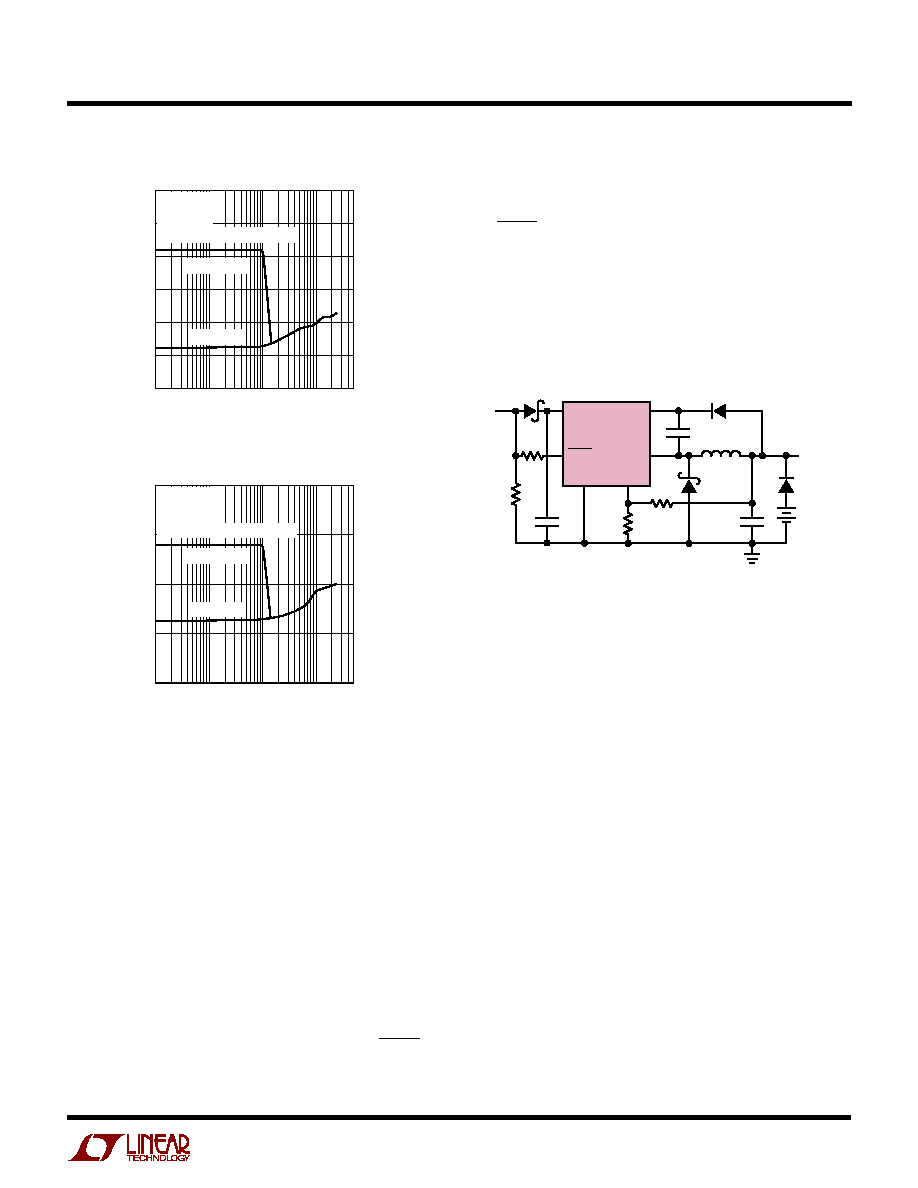
3.3V Step-Down Converter
Efficiency
Burst Mode is a registered trademark of Linear Technology Corporation.
ThinSOT is a trademark of Linear Technology Corporation.
BOOST
V
IN
LT1934
SHDN
1934 TA01
C2
2.2
µ
F
0.22
µ
F
10pF
C1: SANYO 4TPB100M
C2: TAIYO YUDEN GMK325BJ225MN
D1: ON SEMICONDUCTOR MBR0540
D2: CENTRAL CMDSH-3
L1: SUMIDA CDRH4D28-470
V
OUT
3.3V
250mA
D2
604k
1M
L1
47
µ
H
D1
V
IN
4.5V TO 34V
ON OFF
SW
FB
GND
C1
100
µ
F
+
LOAD CURRENT (mA)
60
EFFICIENCY (%)
70
80
90
100
0.1
10
100
1934 TA02
50
1
LT1934
V
IN
= 12V
V
OUT
= 5V
V
OUT
= 3.3V
DESCRIPTIO
U
FEATURES
APPLICATIO S
U
TYPICAL APPLICATIO
U

2
LT1934/LT1934-1
1934f
(Note 1)
Input Voltage (V
IN
) ................................................. 34V
BOOST Pin Voltage ................................................. 40V
BOOST Pin Above SW Pin ...................................... 20V
SHDN Pin ............................................................... 34V
FB Voltage ................................................................ 6V
SW Voltage ............................................................... V
IN
Operating Temperature Range (Note 2) ..........................
LT1934E/LT1934E-1 ......................... ≠ 40
∞
C to 85
∞
C
LT1934I/LT1934I-1 ......................... ≠ 40
∞
C to 125
∞
C
Maximum Junction Temperature .......................... 125
∞
C
Storage Temperature Range ................. ≠ 65
∞
C to 150
∞
C
Lead Temperature (Soldering, 10 sec).................. 300
∞
C
T
JMAX
= 125
∞
C,
JA
= 250
∞
C/ W,
JC
= 102
∞
C/ W
ORDER PART
NUMBER
S6 PART MARKING
LT1934ES6
LT1934ES6-1
LT1934IS6
LT1934IS6-1
LTXP
LTF8
LTAJB
LTAJC
ABSOLUTE AXI U RATI GS
W
W
W
U
PACKAGE/ORDER I FOR ATIO
U
U
W
BOOST 1
GND 2
FB 3
6 SW
5 V
IN
4 SHDN
TOP VIEW
S6 PACKAGE
6-LEAD PLASTIC SOT-23
Consult LTC Marketing for parts specified with wider operating temperature ranges.
PARAMETER
CONDITIONS
MIN
TYP
MAX
UNITS
Undervoltage Lockout
3
3.2
V
≠40
∞
C
T
A
85
∞
C
q
3
3.6
V
≠40
∞
C
T
A
125
∞
C
q
3
3.6
V
Quiescent Current
V
FB
= 1.3V
12
22
µ
A
≠40
∞
C
T
A
85
∞
C
q
12
26
µ
A
≠40
∞
C
T
A
125
∞
C
q
12
26
µ
A
V
SHDN
= 0V
0.01
2
µ
A
FB Comparator Trip Voltage
V
FB
Falling
≠40
∞
C
T
A
85
∞
C
q
1.22
1.25
1.27
V
≠40
∞
C
T
A
125
∞
C
q
1.21
1.25
1.27
V
FB Comparator Hysteresis
10
mV
FB Pin Bias Current
V
FB
= 1.25V
≠40
∞
C
T
A
85
∞
C
q
2
±
15
nA
≠40
∞
C
T
A
125
∞
C
q
2
±
60
nA
FB Voltage Line Regulation
4V < V
IN
< 34V
0.007
%/V
Switch Off Time
V
FB
> 1V
1.4
1.8
2.3
µ
s
V
FB
= 0V
12
µ
s
Maximum Duty Cycle
V
FB
= 1V
≠40
∞
C
T
A
85
∞
C
q
85
88
%
≠40
∞
C
T
A
125
∞
C
q
83
88
%
Switch V
CESAT
I
SW
= 300mA (LT1934)
200
300
mV
I
SW
= 75mA (LT1934-1)
65
120
mV
Switch Current Limit
LT1934
350
400
490
mA
LT1934-1
90
120
160
mA
BOOST Pin Current
I
SW
= 300mA (LT1934)
8.5
12
mA
I
SW
= 75mA (LT1934-1)
6.0
10
mA
Minimum Boost Voltage (Note 3)
I
SW
= 300mA (LT1934)
1.8
2.5
V
I
SW
= 75mA (LT1934-1)
1.7
2.5
V
Switch Leakage Current
2
µ
A
The
q
denotes specifications which apply over the full operating
temperature range, otherwise specifications are at T
A
= 25
∞
C. V
IN
= 10V, V
BOOST
= 15V, unless otherwise noted.
ELECTRICAL CHARACTERISTICS

3
LT1934/LT1934-1
1934f
TYPICAL PERFOR A CE CHARACTERISTICS
U
W
LT1934 Efficiency, V
OUT
= 5V
LT1934 Efficiency, V
OUT
= 3.3V
Current Limit vs Temperature
Off Time vs Temperature
LOAD CURRENT (mA)
60
EFFICIENCY (%)
70
80
90
100
0.1
10
100
1934 G01
50
1
LT1934
V
OUT
= 5V
L = 47
µ
H
T
A
= 25
∞
C
V
IN
= 12V
V
IN
= 24V
LOAD CURRENT (mA)
60
EFFICIENCY (%)
70
80
90
100
0.1
10
100
1934 G02
50
1
LT1934
V
OUT
= 3.3V
L = 47
µ
H
T
A
= 25
∞
C
V
IN
= 24V
V
IN
= 5V
V
IN
= 12V
LOAD CURRENT (mA)
0.1
50
EFFICIENCY (%)
80
90
100
1
10
100
1934 G03
70
60
LT1934-1
V
OUT
= 5V
L = 150
µ
H
T
A
= 25
∞
C
V
IN
= 24V
V
IN
= 12V
LT1934-1 Efficiency, V
OUT
= 5V
LT1934-1 Efficiency, V
OUT
= 3.3V
LOAD CURRENT (mA)
0.1
50
EFFICIENCY (%)
80
90
100
1
10
100
1934 G04
70
60
LT1934-1
V
OUT
= 3.3V
L = 100
µ
H
T
A
= 25
∞
C
V
IN
= 24V
V
IN
= 12V
TEMPERATURE (
∞
C)
≠50
≠25
0
SWITCH CURRENT LIMIT (mA)
200
500
0
50
75
1934 G05
100
400
300
25
100
125
LT1934
LT1934-1
TEMPERATURE (
∞
C)
≠50
OFF TIME (
µ
s)
2.0
2.5
3.0
25
75
1934 G06
1.5
1.0
≠25
0
50
100
125
0.5
0
Note 1: Absolute Maximum Ratings are those values beyond which the life
of the device may be impaired.
Note 2: The LT1934E and LT1934E-1 are guaranteed to meet performance
specifications from 0
∞
C to 70
∞
C. Specifications over the ≠40
∞
C to 85
∞
C
operating temperature range are assured by design, characterization and
correlation with statistical process controls. The LT1934I and LT1934I-1
specifications are guaranteed over the ≠40
∞
C to 125
∞
C temperature range.
Note 3: This is the minimum voltage across the boost capacitor needed to
guarantee full saturation of the internal power switch.
The
q
denotes specifications which apply over the full operating
temperature range, otherwise specifications are at T
A
= 25
∞
C. V
IN
= 10V, V
BOOST
= 15V, unless otherwise noted.
ELECTRICAL CHARACTERISTICS
PARAMETER
CONDITIONS
MIN
TYP
MAX
UNITS
SHDN Pin Current
V
SHDN
= 2.3V
0.5
µ
A
V
SHDN
= 34V
1.5
5
µ
A
SHDN Input Voltage High
2.3
V
SHDN Input Voltage Low
0.25
V

4
LT1934/LT1934-1
1934f
TYPICAL PERFOR A CE CHARACTERISTICS
U
W
Quiescent Current
vs Temperature
Undervoltage Lockout
vs Temperature
Minimum Input Voltage
V
OUT
= 3.3V
Minimum Input Voltage
V
OUT
= 5V
TEMPERATURE (
∞
C)
≠50
0
QUIESCENT CURRENT (
µ
A)
5
10
15
20
≠25
0
25
50
1934 G10
75
100
125
TEMPERATURE (
∞
C)
≠50
2.0
UVLO (V)
2.5
3.0
3.5
4.0
≠25
0
25
50
1934 G11
75
100
125
LOAD CURRENT (mA)
3.5
INPUT VOLTAGE (V)
4.0
4.5
5.0
5.5
6.0
0.1
10
100
1934 G12
3.0
1
LT1934
V
OUT
= 3.3V
T
A
= 25
∞
C
BOOST DIODE TIED TO OUTPUT
V
IN
TO START
V
IN
TO RUN
LOAD CURRENT (mA)
5
INPUT VOLTAGE (V)
6
7
8
0.1
10
100
1934 G13
4
1
LT1934
V
OUT
= 5V
T
A
= 25
∞
C
BOOST DIODE TIED TO OUTPUT
V
IN
TO START
V
IN
TO RUN
Frequency Foldback
V
FB
vs Temperature
SHDN Bias Current
vs SHDN Voltage
FEEDBACK PIN VOLTAGE (V)
0
SWITCH OFF TIME (
µ
s)
6
8
10
0.6
1.0
1934 G07
4
2
0
0.2
0.4
0.8
12
14
16
1.2
T
A
= 25
∞
C
TEMPERATURE (
∞
C)
≠50
≠25
1.22
FEEDBACK VOLTAGE (V)
1.24
1.27
0
50
75
1934 G08
1.23
1.26
1.25
25
100
125
SHDN PIN VOLTAGE (V)
0
0
SHDN PIN CURRENT (
µ
A)
0.5
1.0
1.5
2.0
2
4
6
8
1934 G09
10
12
T
A
= 25
∞
C

5
LT1934/LT1934-1
1934f
U
U
U
PI FU CTIO S
BOOST (Pin 1): The BOOST pin is used to provide a drive
voltage, higher than the input voltage, to the internal
bipolar NPN power switch.
GND (Pin 2): Tie the GND pin to a local ground plane below
the LT1934 and the circuit components. Return the feed-
back divider to this pin.
FB (Pin 3): The LT1934 regulates its feedback pin to 1.25V.
Connect the feedback resistor divider tap to this pin. Set
the output voltage according to V
OUT
= 1.25V (1 + R1/R2)
or R1 = R2 (V
OUT
/1.25 ≠ 1).
SHDN (Pin 4): The SHDN pin is used to put the LT1934 in
shutdown mode. Tie to ground to shut down the LT1934.
Apply 2.3V or more for normal operation. If the shutdown
feature is not used, tie this pin to the V
IN
pin.
V
IN
(Pin 5): The V
IN
pin supplies current to the LT1934's
internal regulator and to the internal power switch. This
pin must be locally bypassed.
SW (Pin 6): The SW pin is the output of the internal power
switch. Connect this pin to the inductor, catch diode and
boost capacitor.
BLOCK DIAGRA
W
≠
+
≠
+
12
µ
s DELAY
ON TIME
OFF TIME
1.8
µ
s DELAY
R
S
Q
BOOST
SW
FB
R2
R1
1934 BD
V
OUT
L1
D2
C3
C1
D1
Q
1
6
3
V
IN
C2
+
V
IN
ON OFF
GND
ENABLE
FEEDBACK
COMPARATOR
5
2
SHDN
4
V
REF
1.25V
6
LT1934/LT1934-1
1934f
OPERATIO
U
The LT1934 uses Burst Mode control, combining both low
quiescent current operation and high switching frequency,
which result in high efficiency across a wide range of load
currents and a small total circuit size.
A comparator monitors the voltage at the FB pin of the
LT1934. If this voltage is higher than the internal 1.25V
reference, the comparator disables the oscillator and power
switch. In this state, only the comparator, reference and
undervoltage lockout circuits are active, and the current
into the V
IN
pin is just 12
µ
A. As the load current discharges
the output capacitor, the voltage at the FB pin falls below
1.25V and the comparator enables the oscillator. The
LT1934 begins to switch, delivering current to the output
capacitor. The output voltage rises, and when it overcomes
the feedback comparator's hysteresis, the oscillator is
disabled and the LT1934 returns to its micropower state.
The oscillator consists of two one-shots and a flip-flop.
A rising edge from the off-time one-shot sets the flip-
flop, which turns on the internal NPN power switch. The
switch remains on until either the on-time one-shot trips
or the current limit is reached. A sense resistor and
amplifier monitor the current through the switch and resets
(Refer to Block Diagram)
the flip-flop when this current reaches 400mA (120mA
for the LT1934-1). After the 1.8
µ
s delay of the off-time
one-shot, the cycle repeats. Generally, the LT1934 will
reach current limit on every cycle--the off time is fixed
and the on time is regulated so that the LT1934 operates
at the correct duty cycle. The 1.8
µ
s off time is lengthened
when the FB pin voltage falls below 0.8V; this foldback
behavior helps control the output current during start-up
and overload. Figure 1 shows several waveforms of an
LT1934 producing 3.3V from a 10V input. When the switch
is on, the SW pin voltage is at 10V. When the switch is off,
the inductor current pulls the SW pin down until it is
clamped near ground by the external catch diode.
The switch driver operates from either the input or from
the BOOST pin. An external capacitor and diode are used
to generate a voltage at the BOOST pin that is higher than
the input supply. This allows the driver to fully saturate the
bipolar switch for efficient operation.
If the SHDN pin is grounded, all internal circuits are turned
off and V
IN
current reduces to the device leakage current,
typically a few nA.
V
OUT
50mV/DIV
V
SW
10V/DIV
Figure 1. Operating Waveforms of the LT1934 Converting
10V to 3.3V at 180mA (Front Page Schematic)
1934 F01a
I
SW
0.5A/DIV
I
LI
0.5A/DIV
5
µ
s/DIV

7
LT1934/LT1934-1
1934f
APPLICATIO S I FOR ATIO
W
U
U
U
Which One to Use: LT1934 or LT1934-1?
The only difference between the LT1934 and LT1934-1 is
the peak current through the internal switch and the
inductor. If your maximum load current is less than 60mA,
use the LT1934-1. If your maximum load is higher, use the
LT1934; it can supply up to ~300mA.
While the LT1934-1 can't deliver as much output current,
it has other advantages. The lower peak switch current
allows the use of smaller components (input capacitor,
inductor and output capacitor). The ripple current at the
input of the LT1934-1 circuit will be smaller and may be an
important consideration if the input supply is current
limited or has high impedance. The LT1934-1's current
draw during faults (output overload or short) and start-up
is lower.
The maximum load current that the LT1934 or LT1934-1
can deliver depends on the value of the inductor used.
Table 1 lists inductor value, minimum output capacitor
and maximum load for 3.3V and 5V circuits. Increasing the
value of the capacitor will lower the output voltage ripple.
Component selection is covered in more detail in the
following sections.
Minimum Input Voltage
The minimum input voltage required to generate a particu-
lar output voltage is determined by either the LT1934's
undervoltage lockout of ~3V or by its maximum duty
cycle. The duty cycle is the fraction of time that the internal
switch is on and is determined by the input and output
voltages:
DC = (V
OUT
+ V
D
)/(V
IN
≠ V
SW
+ V
D
)
where V
D
is the forward voltage drop of the catch diode
(~0.4V) and V
SW
is the voltage drop of the internal switch
(~0.3V at maximum load for the LT1934, ~0.1V for the
LT1934-1). This leads to a minimum input voltage of:
V
IN(MIN)
= (V
OUT
+ V
D
)/DC
MAX
≠ V
D
+ V
SW
with DC
MAX
= 0.85.
Inductor Selection
A good first choice for the inductor value is:
L = 2.5 ∑ (V
OUT
+ V
D
) ∑ 1.8
µ
s/I
LIM
where I
LIM
is the switch current limit (400mA for the
LT1934 and 120mA for the LT1934-1). This choice pro-
vides a worst-case maximum load current of 250mA
(60mA for the LT1934-1). The inductor's RMS current
rating must be greater than the load current and its
saturation current should be greater than I
LIM
. To keep
efficiency high, the series resistance (DCR) should be less
than 0.3
(1
for the LT1934-1). Table 2 lists several
vendors and types that are suitable.
This simple rule may not provide the optimum value for
your application. If the load current is less, then you can
relax the value of the inductor and operate with higher
ripple current. This allows you to use a physically smaller
inductor, or one with a lower DCR resulting in higher
efficiency. The following provides more details to guide
inductor selection. First, the value must be chosen so that
the LT1934 can supply the maximum load current drawn
from the output. Second, the inductor must be rated
appropriately so that the LT1934 will function reliably and
the inductor itself will not be overly stressed.
Detailed Inductor Selection and
Maximum Load Current
The square wave that the LT1934 produces at its switch
pin results in a triangle wave of current in the inductor. The
LT1934 limits the peak inductor current to I
LIM
. Because
Table 1
MINIMUM
MAXIMUM
PART
V
OUT
L
C
OUT
LOAD
LT1934
3.3V
100
µ
H
100
µ
F
300mA
47
µ
H
47
µ
F
250mA
33
µ
H
33
µ
F
200mA
5V
150
µ
H
47
µ
F
300mA
68
µ
H
33
µ
F
250mA
47
µ
H
22
µ
F
200mA
LT1934-1
3.3V
150
µ
H
15
µ
F
60mA
100
µ
H
10
µ
F
45mA
68
µ
H
10
µ
F
20mA
5V
220
µ
H
10
µ
F
60mA
150
µ
H
4.7
µ
F
45mA
100
µ
H
4.7
µ
F
20mA
8
LT1934/LT1934-1
1934f
APPLICATIO S I FOR ATIO
W
U
U
U
the average inductor current equals the load current, the
maximum load current is:
I
OUT(MAX)
= I
PK
≠
I
L
/2
where I
PK
is the peak inductor current and
I
L
is the peak-
to-peak ripple current in the inductor. The ripple current is
determined by the off time, t
OFF
= 1.8
µ
s, and the inductor
value:
I
L
= (V
OUT
+ V
D
) ∑ t
OFF
/L
I
PK
is nominally equal to I
LIM
. However, there is a slight
delay in the control circuitry that results in a higher peak
current and a more accurate value is:
I
PK
= I
LIM
+ 150ns ∑ (V
IN
≠ V
OUT
)/L
These expressions are combined to give the maximum
load current that the LT1934 will deliver:
I
OUT(MAX)
= 350mA + 150ns ∑ (V
IN
≠ V
OUT
)/L ≠ 1.8
µ
s
∑ (V
OUT
+ V
D
)/2L (LT1934)
I
OUT(MAX)
= 90mA + 150ns ∑ (V
IN
≠ V
OUT
)/L ≠ 1.8
µ
s
∑ (V
OUT
+ V
D
)/2L (LT1934-1)
The minimum current limit is used here to be conserva-
tive. The third term is generally larger than the second
term, so that increasing the inductor value results in a
higher output current. This equation can be used to evalu-
ate a chosen inductor or it can be used to choose L for a
given maximum load current. The simple, single equa-
tion rule given above for choosing L was found by setting
I
L
= I
LIM
/2.5. This results in I
OUT(MAX)
~0.8I
LIM
(ignor-
ing the delay term). Note that this analysis assumes that
the inductor current is continuous, which is true if the
ripple current is less than the peak current or
I
L
< I
PK
.
The inductor must carry the peak current without saturat-
ing excessively. When an inductor carries too much
current, its core material can no longer generate addi-
tional magnetic flux (it saturates) and the inductance
drops, sometimes very rapidly with increasing current.
This condition allows the inductor current to increase at
a very high rate, leading to high ripple current and
decreased overload protection.
Inductor vendors provide current ratings for power induc-
tors. These are based on either the saturation current or on
the RMS current that the inductor can carry without dissi-
pating too much power. In some cases it is not clear which
of these two determine the current rating. Some data
sheets are more thorough and show two current ratings,
one for saturation and one for dissipation. For LT1934
applications, the RMS current rating should be higher than
the load current, while the saturation current should be
higher than the peak inductor current calculated above.
Input Capacitor
Step-down regulators draw current from the input supply
in pulses with very fast rise and fall times. The input
capacitor is required to reduce the resulting voltage ripple
at the LT1934 and to force this switching current into a
tight local loop, minimizing EMI. The input capacitor must
have low impedance at the switching frequency to do this
effectively. A 2.2
µ
F ceramic capacitor (1
µ
F for the
LT1934-1) satisfies these requirements.
If the input source impedance is high, a larger value
capacitor may be required to keep input ripple low. In this
case, an electrolytic of 10
µ
F or more in parallel with a 1
µ
F
ceramic is a good combination. Be aware that the input
Table 2. Inductor Vendors
Vendor
Phone
URL
Part Series
Comments
Murata
(404) 426-1300
www.murata.com
LQH3C
Small, Low Cost, 2mm Height
Sumida
(847) 956-0666
www.sumida.com
CR43
CDRH4D28
CDRH5D28
Coilcraft
(847) 639-6400
www.coilcraft.com
DO1607C
DO1608C
DT1608C
Wurth
(866) 362-6673
www.we-online.com
WE-PD1, 2, 3, 4
Electronics
9
LT1934/LT1934-1
1934f
capacitor is subject to large surge currents if the LT1934
circuit is connected to a low impedance supply, and that
some electrolytic capacitors (in particular tantalum) must
be specified for such use.
Output Capacitor and Output Ripple
The output capacitor filters the inductor's ripple current
and stores energy to satisfy the load current when the
LT1934 is quiescent. In order to keep output voltage ripple
low, the impedance of the capacitor must be low at the
LT1934's switching frequency. The capacitor's equivalent
series resistance (ESR) determines this impedance. Choose
one with low ESR intended for use in switching regulators.
The contribution to ripple voltage due to the ESR is
approximately I
LIM
∑ ESR. ESR should be less than ~150m
for the LT1934 and less than ~500m
for the LT1934-1.
The value of the output capacitor must be large enough to
accept the energy stored in the inductor without a large
change in output voltage. Setting this voltage step equal to
1% of the output voltage, the output capacitor must be:
C
OUT
> 50 ∑ L ∑ (I
LIM
/V
OUT
)
2
For example, an LT1934 producing 3.3V with L = 47
µ
H
requires 33
µ
F. This value can be relaxed if small circuit size
is more important than low output ripple.
Sanyo's POSCAP series in B-case and C-case sizes pro-
vides very good performance in a small package for the
LT1934. Similar performance in traditional tantalum ca-
pacitors requires a larger package (C- or D-case). The
APPLICATIO S I FOR ATIO
W
U
U
U
LT1934-1, with its lower switch current, can use a B-case
tantalum capacitor.
With a high quality capacitor filtering the ripple current
from the inductor, the output voltage ripple is determined
by the hysteresis and delay in the LT1934's feedback
comparator. This ripple can be reduced further by adding
a small (typically 10pF) phase lead capacitor between the
output and the feedback pin.
Ceramic Capacitors
Ceramic capacitors are small, robust and have very low
ESR. However, ceramic capacitors can cause problems
when used with the LT1934.
Not all ceramic capacitors are suitable. X5R and X7R types
are stable over temperature and applied voltage and give
dependable service. Other types (Y5V and Z5U) have very
large temperature and voltage coefficients of capacitance.
In the application circuit they may have only a small
fraction of their nominal capacitance and voltage ripple
may be much larger than expected.
Ceramic capacitors are piezoelectric. The LT1934's switch-
ing frequency depends on the load current, and at light
loads the LT1934 can excite the ceramic capacitor at audio
frequencies, generating audible noise. If this is unaccept-
able, use a high performance electrolytic capacitor at the
output. The input capacitor can be a parallel combination
of a 2.2
µ
F ceramic capacitor and a low cost electrolytic
capacitor. The level of noise produced by the LT1934-1
Table 3. Capacitor Vendors
Vendor
Phone
URL
Part Series
Comments
Panasonic
(714) 373-7366
www.panasonic.com
Ceramic,
Polymer,
EEF Series
Tantalum
Kemet
(864) 963-6300
www.kemet.com
Ceramic,
Tantalum
T494, T495
Sanyo
(408) 749-9714
www.sanyovideo.com
Ceramic,
Polymer,
POSCAP
Tantalum
Murata
(404) 436-1300
www.murata.com
Ceramic
AVX
www.avxcorp.com
Ceramic,
Tantalum
TPS Series
Taiyo Yuden
(864) 963-6300
www.taiyo-yuden.com
Ceramic
10
LT1934/LT1934-1
1934f
APPLICATIO S I FOR ATIO
W
U
U
U
when used with ceramic capacitors will be lower and may
be acceptable.
A final precaution regarding ceramic capacitors concerns
the maximum input voltage rating of the LT1934. A
ceramic input capacitor combined with trace or cable
inductance forms a high quality (under damped) tank
circuit. If the LT1934 circuit is plugged into a live supply,
the input voltage can ring to twice its nominal value,
possibly exceeding the LT1934's rating. This situation is
easily avoided; see the Hot Plugging Safely section.
Catch Diode
A 0.5A Schottky diode is recommended for the catch
diode, D1. The diode must have a reverse voltage rating
equal to or greater than the maximum input voltage. The
ON Semiconductor MBR0540 is a good choice; it is rated
for 0.5A forward current and a maximum reverse voltage
of 40V.
Schottky diodes with lower reverse voltage ratings usually
have a lower forward drop and may result in higher
efficiency with moderate to high load currents. However,
these diodes also have higher leakage currents. This
leakage current mimics a load current at the output and
can raise the quiescent current of the LT1934 circuit,
especially at elevated temperatures.
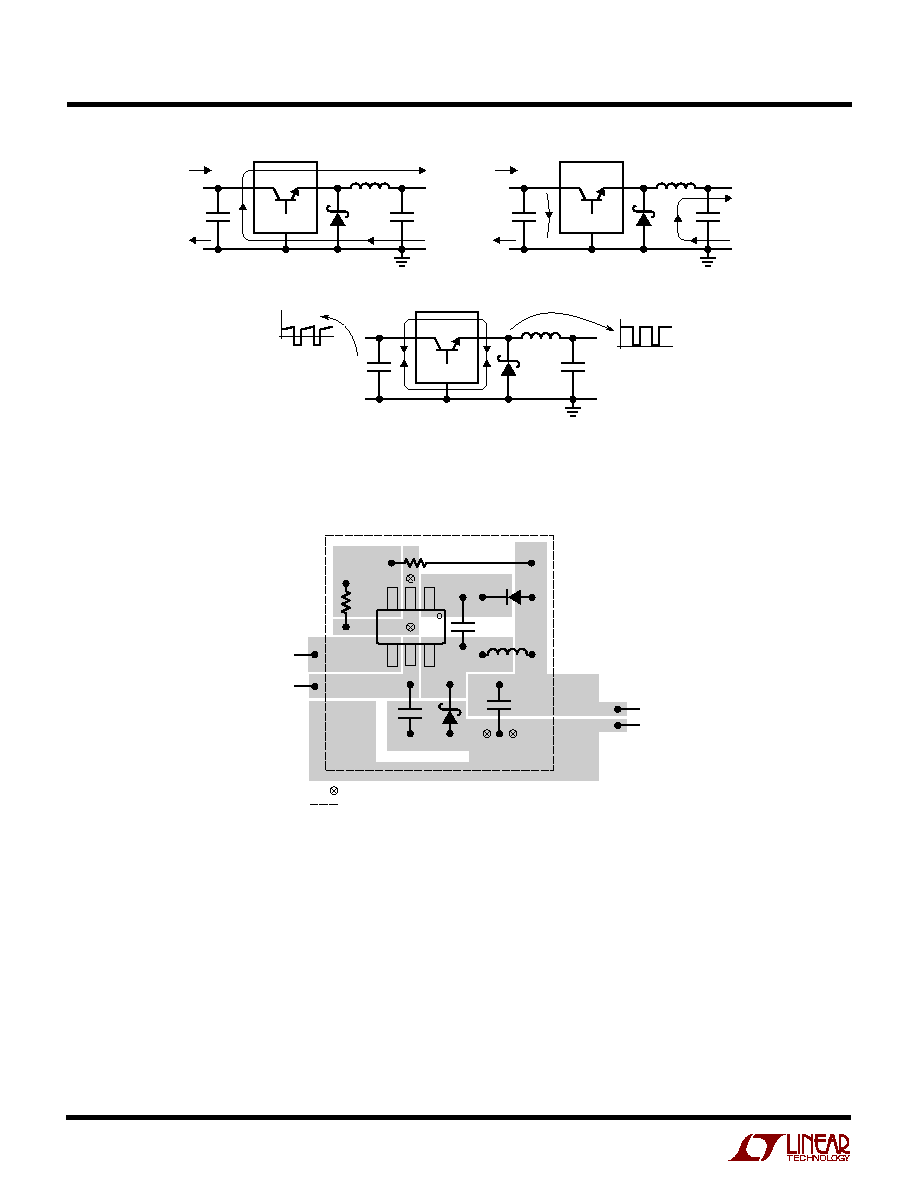
BOOST Pin Considerations
Capacitor C3 and diode D2 are used to generate a boost
voltage that is higher than the input voltage. In most cases
a 0.1
µ
F capacitor and fast switching diode (such as the
1N4148 or 1N914) will work well. Figure 2 shows two
ways to arrange the boost circuit. The BOOST pin must be
more than 2.5V above the SW pin for best efficiency. For
outputs of 3.3V and above, the standard circuit (Figure 2a)
is best. For outputs between 2.8V and 3V, use a 0.22
µ
F
capacitor and a small Schottky diode (such as the
BAT-54). For lower output voltages the boost diode can be
tied to the input (Figure 2b). The circuit in Figure 2a is more
efficient because the BOOST pin current comes from a
lower voltage source. You must also be sure that the
maximum voltage rating of the BOOST pin is not exceeded.
The minimum operating voltage of an LT1934 application
is limited by the undervoltage lockout (~3V) and by the
maximum duty cycle as outlined above. For proper start-
up, the minimum input voltage is also limited by the boost
circuit. If the input voltage is ramped slowly, or the LT1934
is turned on with its SHDN pin when the output is already
in regulation, then the boost capacitor may not be fully
charged. Because the boost capacitor is charged with the
energy stored in the inductor, the circuit will rely on some
minimum load current to get the boost circuit running
properly. This minimum load will depend on input and
output voltages, and on the arrangement of the boost
circuit. The minimum load generally goes to zero once the
circuit has started. Figure 3 shows a plot of minimum load
to start and to run as a function of input voltage. In many
cases the discharged output capacitor will present a load
to the switcher which will allow it to start. The plots show
the worst-case situation where V
IN
is ramping very slowly.
Use a Schottky diode (such as the BAT-54) for the lowest
start-up voltage.
At light loads, the inductor current becomes discontinu-
ous and the effective duty cycle can be very high. This
reduces the minimum input voltage to approximately
300mV above V
OUT
. At higher load currents, the inductor
current is continuous and the duty cycle is limited by the
V
IN
BOOST
GND
SW
V
IN
LT1934
(2a)
D2
V
OUT
C3
V
BOOST
≠ V
SW
V
OUT
MAX V
BOOST
V
IN
+ V
OUT
V
IN
BOOST
GND
SW
V
IN
LT1934
(2b)
D2
1934 F02
V
OUT
C3
V
BOOST
≠ V
SW
V
IN
MAX V
BOOST
2V
IN
Figure 2. Two Circuits for Generating the Boost Voltage
11
LT1934/LT1934-1
1934f
APPLICATIO S I FOR ATIO
W
U
U
U
Figure 4. Diode D4 Prevents a Shorted Input from Discharging
a Backup Battery Tied to the Output; It Also Protects the Circuit
from a Reversed Input. The LT1934 Runs Only When the Input
is Present
maximum duty cycle of the LT1934, requiring a higher
input voltage to maintain regulation.
Shorted Input Protection
If the inductor is chosen so that it won't saturate exces-
sively, an LT1934 buck regulator will tolerate a shorted
output. There is another situation to consider in systems
where the output will be held high when the input to the
LT1934 is absent. This may occur in battery charging
applications or in battery backup systems where a battery
or some other supply is diode OR-ed with the LT1934's
output. If the V
IN
pin is allowed to float and the SHDN pin
is held high (either by a logic signal or because it is tied to
V
IN
), then the LT1934's internal circuitry will pull its
quiescent current through its SW pin. This is fine if your
system can tolerate a few mA in this state. If you ground
the SHDN pin, the SW pin current will drop to essentially
zero. However, if the V
IN
pin is grounded while the output
is held high, then parasitic diodes inside the LT1934 can
pull large currents from the output through the SW pin and
the V
IN
pin. Figure 4 shows a circuit that will run only when
the input voltage is present and that protects against a
shorted or reversed input.
V
IN
BOOST
GND
FB
SHDN
SW
5
D4
V
IN
4
1
6
2
3
1M
100k
LT1934
1934 F07
V
OUT
BACKUP
D4: MBR0530
Figure 3. The Minimum Input Voltage Depends
on Output Voltage, Load Current and Boost Circuit
Minimum Input Voltage V
OUT
= 3.3V
Minimum Input Voltage V
OUT
= 5V
LOAD CURRENT (mA)
3.5
INPUT VOLTAGE (V)
4.0
4.5
5.0
5.5
6.0
0.1
10
100
1934 G12
3.0
1
LT1934
V
OUT
= 3.3V
T
A
= 25
∞
C
BOOST DIODE TIED TO OUTPUT
V
IN
TO START
V
IN
TO RUN
LOAD CURRENT (mA)
5
INPUT VOLTAGE (V)
6
7
8
0.1
10
100
1934 G13
4
1
LT1934
V
OUT
= 5V
T
A
= 25
∞
C
BOOST DIODE TIED TO OUTPUT
V
IN
TO START
V
IN
TO RUN
PCB Layout
For proper operation and minimum EMI, care must be
taken during printed circuit board layout. Figure 5 shows
the high current paths in the buck regulator circuit. Note
that large, switched currents flow in the power switch, the
catch diode (D1) and the input capacitor (C2). The loop
formed by these components should be as small as
possible. Furthermore, the system ground should be tied
to the regulator ground in only one place; this prevents the
switched current from injecting noise into the system
ground. These components, along with the inductor and
output capacitor, should be placed on the same side of the
circuit board, and their connections should be made on
that layer. Place a local, unbroken ground plane below
these components, and tie this ground plane to system
ground at one location, ideally at the ground terminal of the
output capacitor C1. Additionally, the SW and BOOST
nodes should be kept as small as possible. Finally, keep
the FB node as small as possible so that the ground pin and
12
LT1934/LT1934-1
1934f
APPLICATIO S I FOR ATIO
W
U
U
U
Figure 6. A Good PCB Layout Ensures Proper, Low EMI Operation
SHUTDOWN
VIAS TO LOCAL GROUND PLANE
OUTLINE OF LOCAL GROUND PLANE
V
IN
V
OUT
1934 F06
SYSTEM
GROUND
Figure 5. Subtracting the Current When the Switch is On (a) from the Current When the Switch is Off (b) Reveals the Path of the High
Frequency Switching Current (c). Keep This Loop Small. The Voltage on the SW and BOOST Nodes Will Also be Switched; Keep These
Nodes as Small as Possible. Finally, Make Sure the Circuit is Shielded with a Local Ground Plane
V
IN
SW
GND
(5a)
V
IN
V
SW
C2
D1
C1
1934 F05
L1
SW
GND
(5c)
V
IN
SW
GND
(5b)
I
C1
ground traces will shield it from the SW and BOOST nodes.
Figure 6 shows component placement with trace, ground
plane and via locations. Include two vias near the GND pin
of the LT1934 to help remove heat from the LT1934 to the
ground plane.
Hot Plugging Safely
The small size, robustness and low impedance of ceramic
capacitors make them an attractive option for the input
bypass capacitor of LT1934 and LT1934-1 circuits. How-
ever, these capacitors can cause problems if the LT1934
is plugged into a live supply (see Linear Technology
Application Note 88 for a complete discussion). The low
loss ceramic capacitor combined with stray inductance in
series with the power source forms an under damped tank
circuit, and the voltage at the V
IN
pin of the LT1934 can ring
to twice the nominal input voltage, possibly exceeding the
LT1934's rating and damaging the part. If the input supply
is poorly controlled or the user will be plugging the LT1934
into an energized supply, the input network should be
designed to prevent this overshoot.
13
LT1934/LT1934-1
1934f
APPLICATIO S I FOR ATIO
W
U
U
U
+
LT1934
2.2
µ
F
V
IN
10V/DIV
I
IN
10A/DIV
10
µ
s/DIV
V
IN
CLOSING SWITCH
SIMULATES HOT PLUG
I
IN
(7a)
(7b)
(7c)
(7d)
(7e)
LOW
IMPEDANCE
ENERGIZED
24V SUPPLY
STRAY
INDUCTANCE
DUE TO 6 FEET
(2 METERS) OF
TWISTED PAIR
+
LT1934
2.2
µ
F
10
µ
F
35V
AI.EI.
LT1934
2.2
µ
F
0.1
µ
F
1
LT1934-1
1
µ
F
LT1934-1
1
µ
F
1934 F07
0.1
µ
F
4.7
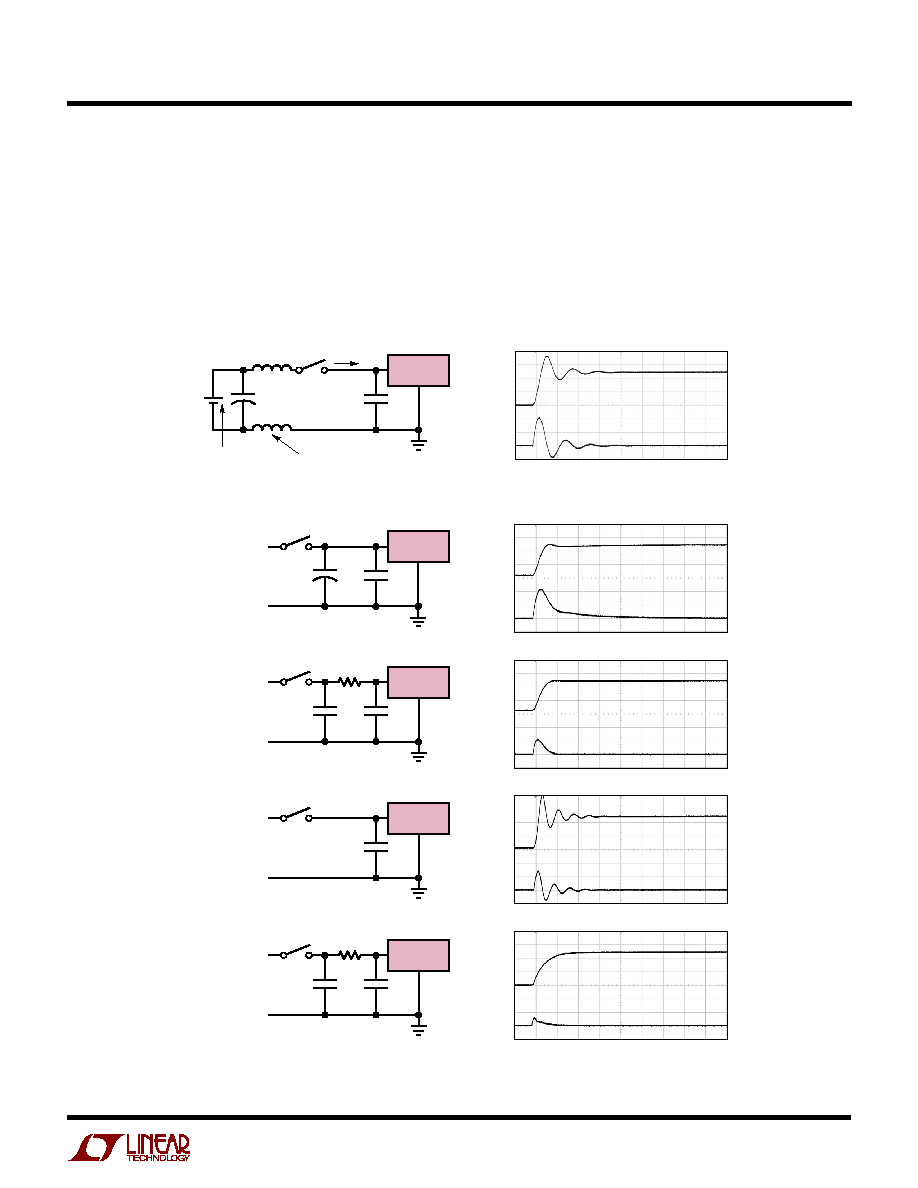
Figure 7. A Well Chosen Input Network Prevents Input Voltage Overshoot and
Ensures Reliable Operation When the LT1934 is Connected to a Live Supply
Figure 7 shows the waveforms that result when an LT1934
circuit is connected to a 24V supply through six feet of
24-gauge twisted pair. The first plot is the response with
a 2.2
µ
F ceramic capacitor at the input. The input voltage
rings as high as 35V and the input current peaks at 20A.
One method of damping the tank circuit is to add another
capacitor with a series resistor to the circuit. In Figure 7b
an aluminum electrolytic capacitor has been added. This
capacitor's high equivalent series resistance damps the
circuit and eliminates the voltage overshoot. The extra
capacitor improves low frequency ripple filtering and can
slightly improve the efficiency of the circuit, though it is
likely to be the largest component in the circuit. An
alternative solution is shown in Figure 7c. A 1
resistor is

14
LT1934/LT1934-1
1934f
added in series with the input to eliminate the voltage
overshoot (it also reduces the peak input current). A 0.1
µ
F
capacitor improves high frequency filtering. This solution
is smaller and less expensive than the electrolytic capaci-
tor. For high input voltages its impact on efficiency is
minor, reducing efficiency less than one half percent for a
5V output at full load operating from 24V.
Voltage overshoot gets worse with reduced input capaci-
tance. Figure 7d shows the hot plug response with a 1
µ
F
ceramic input capacitor, with the input ringing above 40V.
The LT1934-1 can tolerate a larger input resistance, such
as shown in Figure 7e where a 4.7
resistor damps the
voltage transient and greatly reduces the input current
glitch on the 24V supply.
High Temperature Considerations
The die temperature of the LT1934 must be lower than the
maximum rating of 125
∞
C. This is generally not a concern
unless the ambient temperature is above 85
∞
C. For higher
temperatures, care should be taken in the layout of the
circuit to ensure good heat sinking of the LT1934. The
maximum load current should be derated as the ambient
temperature approaches 125
∞
C.
The die temperature is calculated by multiplying the LT1934
power dissipation by the thermal resistance from junction
to ambient. Power dissipation within the LT1934 can be
APPLICATIO S I FOR ATIO
W
U
U
U
estimated by calculating the total power loss from an
efficiency measurement and subtracting the catch diode
loss. The resulting temperature rise at full load is nearly
independent of input voltage. Thermal resistance depends
on the layout of the circuit board, but a value of 150
∞
C/W
is typical.
The temperature rise for an LT1934 producing 5V at
250mA is approximately 25
∞
C, allowing it to deliver full
load to 100
∞
C ambient. Above this temperature the load
current should be reduced. For 3.3V at 250mA the tem-
perature rise is 15
∞
C.
Finally, be aware that at high ambient temperatures the
external Schottky diode, D1, is likely to have significant
leakage current, increasing the quiescent current of the
LT1934 converter.
Outputs Greater Than 6V
For outputs greater than 6V, tie a diode (such as a 1N4148)
from the SW pin to V
IN
to prevent the SW pin from ringing
above V
IN
during discontinuous mode operation. The 12V
output circuit in Typical Applications shows the location of
this diode. Also note that for outputs above 6V, the input
voltage range will be limited by the maximum rating of the
BOOST pin. The 12V circuit shows how to overcome this
limitation using an additional Zener diode.

15
LT1934/LT1934-1
1934f
TYPICAL APPLICATIO S
U
3.3V Step-Down Converter
BOOST
V
IN
LT1934-1
SHDN
1934 TA04
C2
1
µ
F
0.1
µ
F
10pF
C1: TAIYO YUDEN JMK316BJ226ML
C2: TAIYO YUDEN GMK316BJ105ML
D1: ZETEX ZHCS400 OR ON SEMI MBR0540
D2: CENTRAL CMDSH-3
L1: COILCRAFT DO1608C-104 OR
WURTH ELECTRONICS WE-PD4 TYPE S
V
OUT
3.3V
45mA
D2
604k
1M
L1
100
µ
H
D1
V
IN
4.5V TO 34V
ON OFF
SW
FB
GND
C1
22
µ
F
+
5V Step-Down Converter
BOOST
V
IN
LT1934-1
SHDN
1934 TA05
C2
1
µ
F
0.1
µ
F
10pF
C1: TAIYO YUDEN JMK316BJ226ML
C2: TAIYO YUDEN GMK316BJ105ML
D1: ZETEX ZHCS400 OR ON SEMI MBR0540
D2: CENTRAL CMPD914
L1: COILCRAFT DO1608C-154 OR
WURTH ELECTRONICS WE-PD4 TYPE S
V
OUT
5V
45mA
D2
332k
1M
L1
150
µ
H
D1
V
IN
6.5V TO 34V
ON OFF
SW
FB
GND
C1
22
µ
F
+
16
LT1934/LT1934-1
1934f
1.8V Step-Down Converter
BOOST
V
IN
LT1934
SHDN
1934 TA06
C2
2.2
µ
F
0.1
µ
F
C1: SANYO 2R5TPB100M
C2: TAIYO YUDEN EMK316BJ225ML
D1: ZETEX ZHCS400 OR ON SEMI MBR0540
D2: CENTRAL CMPD914
L1: SUMIDA CR43-330
V
OUT
1.8V
250mA
D2
332k
147k
L1
33
µ
H
D1
V
IN
3.6V TO 16V
ON OFF
SW
FB
GND
C1
100
µ
F
+
BOOST
V
IN
LT1934-1
SHDN
1934 TA08
1
µ
F
D4
10V
C1
10pF
D1: ON SEMICONDUCTOR MBR0540
D2, D3: BAT54
D4: CENTRAL CMPZ5240B
L1: COILTRONICS CTX50-1
ZENER DIODE D4 PROVIDES AN UNDERVOLTAGE LOCKOUT,
REDUCING THE INPUT CURRENT REQUIRED AT START-UP
V
OUT
3V
9mA
ISOLATED
OUT
3V
3mA
D2
D3
715k
390k
1M
L1A
50
µ
H
L1B
50
µ
H
D1
V
IN
14V TO 32V
<3.6mA
SW
FB
GND
33
µ
F
+
∑
∑
10
µ
F
+
Loop Powered 3.3V Supply with Additional Isolated Output
TYPICAL APPLICATIO S
U

17
LT1934/LT1934-1
1934f
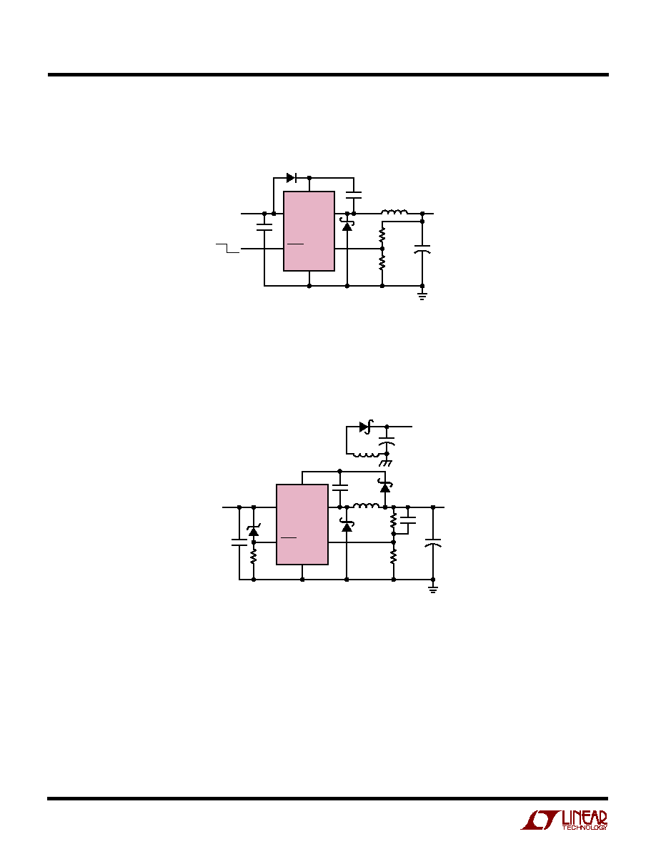
Standalone 350mA Li-Ion Battery Charger
BOOST
V
IN
LT1934
SHDN
1934 TA07a
C2
1
µ
F
D3
0.1
µ
F
C1: SANYO 6TPB47M
(619) 661-6835
C2: TAIYO YUDEN GMK316BJ105ML
(408) 573-4150
D1, D3: ON SEMICONDUCTOR MBR0540
(602) 244-6600
D2: CENTRAL CMDSH-3
(516) 435-1110
L1: SUMIDA CR43-470
(847) 956-0667
D2
332k
1M
1k
1k
10k
L1
47
µ
H
D1
V
IN
7V TO 28V
SW
FB
GND
V
IN
CHRG
LTC4052
ACPR
GATE
SENSE
BAT
350mA
1-CELL 4.2V
Li-Ion
BATTERY
GND
TIMER
C1
47
µ
F
CHARGE STATUS
AC PRESENT
+
C5
10
µ
F
+
0.047
µ
F
C
TIMER
0.1
µ
F
0.022
µ
F
BATTERY VOLTAGE (V)
2.5
CHARGE CURRENT (mA)
200
300
4.5
1934 TA07b
100
0
3
3.5
4
500
400
V
IN
= 12V
V
IN
= 8V
V
IN
= 24V
TYPICAL APPLICATIO S
U
18
LT1934/LT1934-1
1934f
TYPICAL APPLICATIO S
U
12V Step-Down Converter
BOOST
V
IN
LT1934
SHDN
1934 TA09
C2
2.2
µ
F
0.1
µ
F
C1: KEMET T495D226K020AS
C2: TAIYO YUDEN GMK325BJ225MN
D1: ON SEMI MBR0540
D2, D4: CENTRAL CMPD914
D3: CENTRAL CMPZ5234B 6.2V ZENER
L1: TDK SLF6028T-101MR42
V
OUT
12V
170mA
D4
100k
866k
L1
100
µ
H
D1
V
IN
15V TO 32V
ON OFF
SW
FB
GND
D2
D3
C1
22
µ
F
+
19
LT1934/LT1934-1
1934f
PACKAGE DESCRIPTIO
N
U
S6 Package
6-Lead Plastic TSOT-23
(Reference LTC DWG # 05-08-1636)
Information furnished by Linear Technology Corporation is believed to be accurate and reliable.
However, no responsibility is assumed for its use. Linear Technology Corporation makes no represen-
tation that the interconnection of its circuits as described herein will not infringe on existing patent rights.
1.50 ≠ 1.75
(NOTE 4)
2.80 BSC
0.30 ≠ 0.45
6 PLCS (NOTE 3)
DATUM `A'
0.09 ≠ 0.20
(NOTE 3)
S6 TSOT-23 0302
2.90 BSC
(NOTE 4)
0.95 BSC
1.90 BSC
0.80 ≠ 0.90
1.00 MAX
0.01 ≠ 0.10
0.20 BSC
0.30 ≠ 0.50 REF
PIN ONE ID
NOTE:
1. DIMENSIONS ARE IN MILLIMETERS
2. DRAWING NOT TO SCALE
3. DIMENSIONS ARE INCLUSIVE OF PLATING
4. DIMENSIONS ARE EXCLUSIVE OF MOLD FLASH AND METAL BURR
5. MOLD FLASH SHALL NOT EXCEED 0.254mm
6. JEDEC PACKAGE REFERENCE IS MO-193
3.85 MAX
0.62
MAX
0.95
REF
RECOMMENDED SOLDER PAD LAYOUT
PER IPC CALCULATOR
1.4 MIN
2.62 REF
1.22 REF

20
LT1934/LT1934-1
1934f
LT/TP 0703 1K ∑ PRINTED IN USA
©
LINEAR TECHNOLOGY CORPORATION 2002
RELATED PARTS
Linear Technology Corporation
1630 McCarthy Blvd., Milpitas, CA 95035-7417
(408) 432-1900
q
FAX: (408) 434-0507
q
www.linear.com
PART NUMBER
DESCRIPTION
COMMENTS
LT1616
25V, 500mA (I
OUT
), 1.4MHz, High Efficiency
V
IN
= 3.6V to 25V, V
OUT
= 1.25V, I
Q
= 1.9mA, I
SD
= <1
µ
A,
Step-Down DC/DC Converter
ThinSOT Package
LT1676
60V, 440mA (I
OUT
), 100kHz, High Efficiency
V
IN
= 7.4V to 60V, V
OUT
= 1.24V, I
Q
= 3.2mA, I
SD
= 2.5
µ
A,
Step-Down DC/DC Converter
S8 Package
LT1765
25V, 2.75A (I
OUT
), 1.25MHz, High Efficiency
V
IN
= 3V to 25V, V
OUT
= 1.2V, I
Q
= 1mA, I
SD
= 15
µ
A,
Step-Down DC/DC Converter
S8, TSSOP16E Packages
LT1766
60V, 1.2A (I
OUT
), 200kHz, High Efficiency
V
IN
= 5.5V to 60V, V
OUT
= 1.2V, I
Q
= 2.5mA, I
SD
= 25
µ
A,
Step-Down DC/DC Converter
TSSOP16/E Package
LT1767
25V, 1.2A (I
OUT
), 1.25MHz, High Efficiency
V
IN
= 3V to 25V; V
OUT
= 1.2V, I
Q
= 1mA, I
SD
= 6
µ
A,
Step-Down DC/DC Converter
MS8/E Packages
LT1776
40V, 550mA (I
OUT
), 200kHz, High Efficiency
V
IN
= 7.4V to 40V; V
OUT
= 1.24V, I
Q
= 3.2mA, I
SD
= 30
µ
A,
Step-Down DC/DC Converter
N8, S8 Packages
LTC
Æ
1877
600mA (I
OUT
), 550kHz, Synchronous
V
IN
= 2.7V to 10V; V
OUT
= 0.8V, I
Q
= 10
µ
A, I
SD
= <1
µ
A,
Step-Down DC/DC Converter
MS8 Package
LTC1879
1.2A (I
OUT
), 550kHz, Synchronous
V
IN
= 2.7V to 10V; V
OUT
= 0.8V, I
Q
= 15
µ
A, I
SD
= <1
µ
A,
Step-Down DC/DC Converter
TSSOP16 Package
LT1956
60V, 1.2A (I
OUT
), 500kHz, High Efficiency
V
IN
= 5.5V to 60V, V
OUT
= 1.2V, I
Q
= 2.5mA, I
SD
= 25
µ
A,
Step-Down DC/DC Converter
TSSOP16/E Package
LTC3405/LTC3405A
300mA (I
OUT
), 1.5MHz, Synchronous
V
IN
= 2.7V to 6V, V
OUT
= 0.8V, I
Q
= 20
µ
A, I
SD
= <1
µ
A,
Step-Down DC/DC Converter
ThinSOT Package
LTC3406/LTC3406B
600mA (I
OUT
), 1.5MHz, Synchronous
V
IN
= 2.5V to 5.5V, V
OUT
= 0.6V, I
Q
= 20
µ
A, I
SD
= <1
µ
A,
Step-Down DC/DC Converter
ThinSOT Package
LTC3411
1.25A (I
OUT
), 4MHz, Synchronous
V
IN
= 2.5V to 5.5V, V
OUT
= 0.8V, I
Q
= 60
µ
A, I
SD
= <1
µ
A,
Step-Down DC/DC Converter
MS Package
LTC3412
2.5A (I
OUT
), 4MHz, Synchronous
V
IN
= 2.5V to 5.5V, V
OUT
= 0.8V, I
Q
= 60
µ
A, I
SD
= <1
µ
A,
Step-Down DC/DC Converter
TSSOP16E Package
LTC3430
60V, 2.75A (I
OUT
), 200kHz, High Efficiency
V
IN
= 5.5V to 60V, V
OUT
= 1.2V, I
Q
= 2.5mA, I
SD
= 30
µ
A,
Step-Down DC/DC Converter
TSSOP16E Package
5V Step-Down Converter
BOOST
V
IN
LT1934
SHDN
1934 TA03
C2
2.2
µ
F
0.1
µ
F
10pF
C1: SANYO 6TPB68M
C2: TAIYO YUDEN GMK325BJ225MN
D1: ZETEX ZHCS400 OR ON SEMI MBR0540
D2: CENTRAL CMPD914
L1: SUMIDA CDRH5D28-680
V
OUT
5V
250mA
D2
332k
1M
L1
68
µ
H
D1
V
IN
6.5V TO 34V
ON OFF
SW
FB
GND
C1
68
µ
F
+
TYPICAL APPLICATIO
U