 | ÐлекÑÑоннÑй компоненÑ: LT3027IDD | СкаÑаÑÑ:  PDF PDF  ZIP ZIP |
Äîêóìåíòàöèÿ è îïèñàíèÿ www.docs.chipfind.ru
1
LT3027
3027f
V
OUT
100µV/DIV
20µV
RMS
3027 TA01b
APPLICATIO S
U
DESCRIPTIO
U
FEATURES
TYPICAL APPLICATIO
U
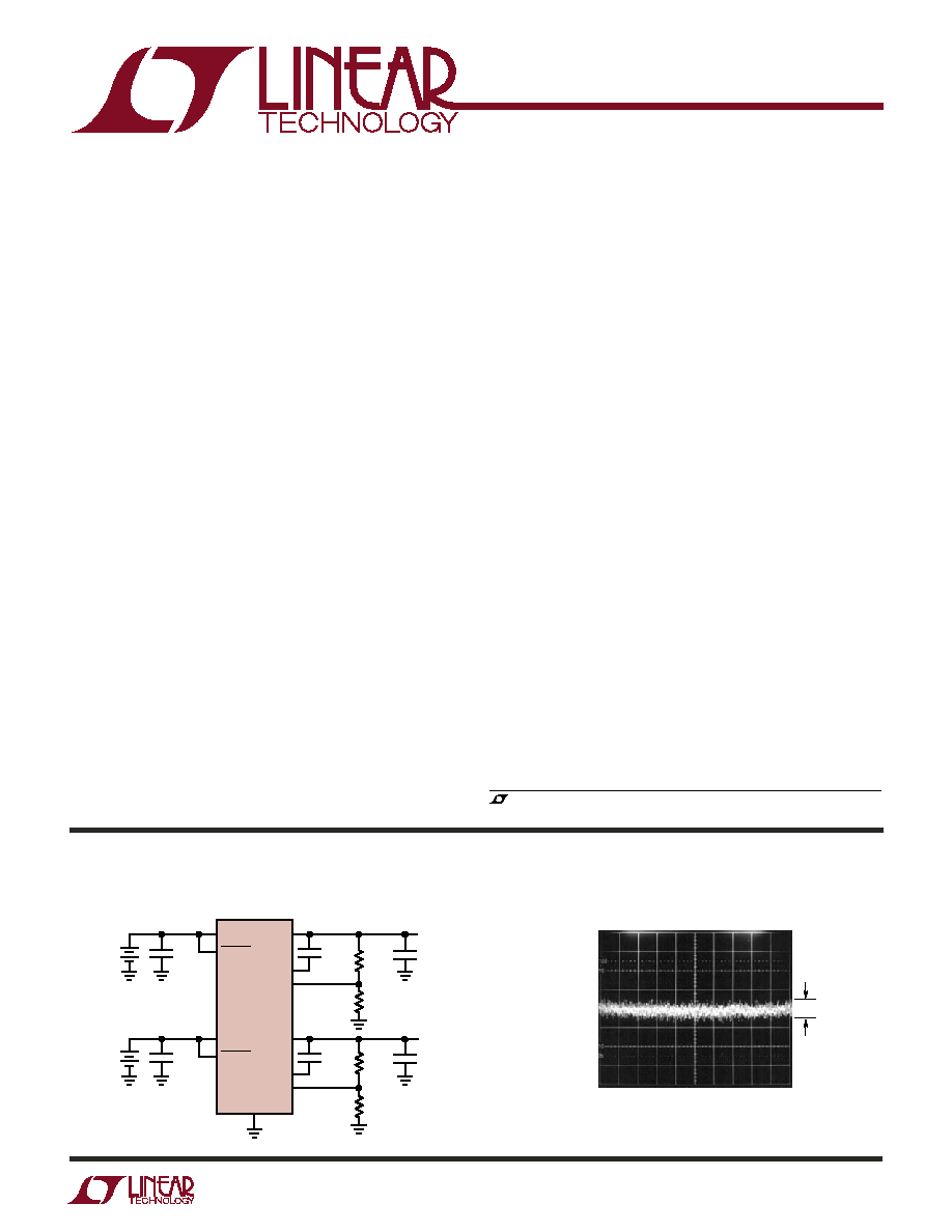
Dual 100mA,
Low Dropout, Low Noise,
Micropower Regulator with
Independent Inputs
Low Noise: 20µV
RMS
(10Hz to 100kHz)
Low Quiescent Current: 25µA/Channel
Independent Inputs
Wide Input Voltage Range: 1.8V to 20V
Output Current: 100mA/Channel
Very Low Shutdown Current: <0.1
µ
A
Low Dropout Voltage: 300mV at 100mA
Adjustable Output from 1.22V to 20V
Stable with 1µF Output Capacitor
Stable with Aluminum, Tantalum or
Ceramic Capacitors
Reverse Battery Protected
No Protection Diodes Needed
Overcurrent and Overtemperature Protected
Thermally Enhanced 10-Lead MSOP and DFN
Packages
The LT
®
3027 is a dual, micropower, low noise, low drop-
out regulator with independent inputs. With an external
0.01µF bypass capacitor, output noise is a low 20µV
RMS
over a 10Hz to 100kHz bandwidth. Designed for use in
battery-powered systems, the low 25µA quiescent current
per channel makes it an ideal choice. In shutdown, quies-
cent current drops to less than 0.1µA. Shutdown control
is independent for each channel, allowing for flexibility in
power management. The device is capable of operating
over an input voltage from 1.8V to 20V, and can supply
100mA of output current from each channel with a drop-
out voltage of 300mV. Quiescent current is well controlled
in dropout.
The LT3027 regulator is stable with output capacitors as
low as 1µF. Small ceramic capacitors can be used without
the series resistance required by other regulators.
Internal protection circuitry includes reverse battery pro-
tection, current limiting and thermal limiting protection.
The device is available as an adjustable device with a
1.22V reference voltage. The LT3027 regulator is available
in the thermally enhanced 10-lead MSOP and low profile
(0.75mm) 3mm × 3mm DFN packages.
10Hz to 100kHz Output Noise
3.3V/2.5V Low Noise Regulators
Cellular Phones
Pagers
Battery-Powered Systems
Frequency Synthesizers
Wireless Modems
, LTC and LT are registered trademarks of Linear Technology Corporation.
IN1
0.01µF
0.01µF
10µF
3027 TA01
OUT1
V
IN1
3.7V TO
20V
BYP1
ADJ1
OUT2
BYP2
ADJ2
GND
LT3027
3.3V AT 100mA
20µV
RMS
NOISE
2.5V AT 100mA
20µV
RMS
NOISE
1µF
SHDN1
IN2
V
IN2
2.9V TO
20V
1µF
SHDN2
10µF
422k
249k
261k
249k
Protected by U.S. Patents, including 6118263, 6144250.
2
LT3027
3027f
(Note 1)
IN1, IN2 Pin Voltage .............................................. ±20V
OUT1, OUT2 Pin Voltage ....................................... ±20V
Input to Output Differential Voltage ....................... ±20V
ADJ1, ADJ2 Pin Voltage ......................................... ±7V
BYP1, BYP2 Pin Voltage ....................................... ±0.6V
SHDN1, SHDN2 Pin Voltage ................................. ±20V
Output Short-Circut Duration .......................... Indefinite
PARAMETER
CONDITIONS
MIN
TYP
MAX
UNITS
Minimum Input Voltage
I
LOAD
= 100mA
1.8
2.3
V
(Notes 3, 10)
ADJ1, ADJ2 Pin Voltage
V
IN
= 2V, I
LOAD
= 1mA
1.205
1.220
1.235
V
(Note 3, 4)
2.3V < V
IN
< 20V, 1mA < I
LOAD
< 100mA
1.190
1.220
1.250
V
Line Regulation (Note 3)
V
IN
= 2V to 20V, I
LOAD
= 1mA
1
10
mV
Load Regulation (Note 3)
V
IN
= 2.3V, I
LOAD
= 1mA to 100mA
1
12
mV
V
IN
= 2.3V, I
LOAD
= 1mA to 100mA
25
mV
Dropout Voltage
I
LOAD
= 1mA
0.10
0.15
V
V
IN
= V
OUT(NOMINAL)
I
LOAD
= 1mA
0.19
V
(Notes 5, 6, 10)
I
LOAD
= 10mA
0.17
0.22
V
I
LOAD
= 10mA
0.29
V
I
LOAD
= 50mA
0.24
0.28
V
I
LOAD
= 50mA
0.38
V
I
LOAD
= 100mA
0.30
0.35
V
I
LOAD
= 100mA
0.45
V
The
denotes specifications which apply over the full operating temperature range, otherwise specifications are T
A
= 25°C. (Note 2)
Consult factory for parts specified with wider operating temperature ranges.
ABSOLUTE AXI U RATI GS
W
W
W
U
PACKAGE/ORDER I FOR ATIO
U
U
W
ELECTRICAL CHARACTERISTICS
LT3027EDD
LT3027IDD
ORDER PART
NUMBER
DD PART
MARKING
Operating Junction Temperature Range
(Note 2) ............................................ 40°C to 125°C
Storage Temperature Range
DD Package ...................................... 65°C to 125°C
MSE Package ................................... 65°C to 150°C
Lead Temperature (Soldering, 10 sec).................. 300°C
TOP VIEW
DD PACKAGE
10-LEAD (3mm × 3mm) PLASTIC DFN
EXPOSED PAD (PIN 11) IS GND
MUST BE SOLDERED TO PCB
10
9
6
7
8
4
5
3
2
1
OUT2
IN2
IN1
SHDN1
OUT1
BYP2
ADJ2
SHDN2
ADJ1
BYP1
11
1
2
3
4
5
BYP2
ADJ2
SHDN2
ADJ1
BYP1
10
9
8
7
6
OUT2
IN2
IN1
SHDN1
OUT1
TOP VIEW
MSE PACKAGE
10-LEAD PLASTIC MSOP
EXPOSED PAD (PIN 11) IS GND
MUST BE SOLDERED TO PCB
11
LT3027EMSE
LT3027IMSE
ORDER PART
NUMBER
MSE PART
MARKING
T
JMAX
= 125°C,
JA
= 43°C/ W,
JC
= 3°C/ W
T
JMAX
= 150°C,
JA
= 40°C/ W,
JC
= 10°C/ W
LBKN
LBMC
LTBKK
LTBMD
3
LT3027
3027f
PARAMETER
CONDITIONS
MIN
TYP
MAX
UNITS
GND Pin Current (Per Channel)
I
LOAD
= 0mA
25
50
µA
V
IN
= V
OUT(NOMINAL)
I
LOAD
= 1mA
60
120
µA
(Notes 5, 7)
I
LOAD
= 10mA
250
400
µA
I
LOAD
= 50mA
1
2
mA
I
LOAD
= 100mA
2.4
4
mA
Output Voltage Noise
C
OUT
= 10µF, C
BYP
= 0.01µF, I
LOAD
= 100mA, BW = 10Hz to 100kHz
20
µV
RMS
ADJ1/ADJ2 Pin Bias Current
(Notes 3, 8)
30
100
nA
Shutdown Threshold
V
OUT
= Off to On
0.8
1.4
V
V
OUT
= On to Off
0.25
0.65
V
SHDN1/SHDN2 Pin Current
V
SHDN
= 0V
0
0.5
µA
(Note 9)
V
SHDN
= 20V
1
3
µA
Quiescent Current in Shutdown
V
IN
= 6V, V
SHDN
= 0V (Both SHDN Pins)
0.01
0.1
µA
Ripple Rejection (Note 3)
V
IN
= 2.72V (Avg), V
RIPPLE
= 0.5V
P-P
, f
RIPPLE
= 120Hz,
55
65
dB
I
LOAD
= 100mA
Current Limit
V
IN
= 7V, V
OUT
= 0V
200
mA
V
IN
= 2.3V, V
OUT
= 5%
110
mA
Input Reverse Leakage Current
V
IN
= 20V, V
OUT
= 0V
1
mA
The
denotes specifications which apply over the full operating temperature range, otherwise specifications are T
A
= 25°C. (Note 2)
ELECTRICAL CHARACTERISTICS
Note 5: To satisfy requirements for minimum input voltage, the LT3027 is
tested and specified for these conditions with an external resistor divider
(two 250k resistors) for an output voltage of 2.44V. The external resistor
divider will add a 5µA DC load on the output.
Note 6: Dropout voltage is the minimum input to output voltage differential
needed to maintain regulation at a specified output current. In dropout, the
output voltage will be equal to: V
IN
V
DROPOUT
.
Note 7: GND pin current is tested with V
IN
= 2.44V and a current source
load. This means the device is tested while operating in its dropout region
or at the minimum input voltage specification. This is the worst-case GND
pin current. The GND pin current will decrease slightly at higher input
voltages.
Note 8: ADJ1 and ADJ2 pin bias current flows into the pin.
Note 9: SHDN1 and SHDN2 pin current flows into the pin.
Note 10: For the LT3027 dropout voltage will be limited by the minimum
input voltage specification under some output voltage/load conditions. See
the curve of Minimum Input Voltage in the Typical Performance
Characteristics.
Note 1: Absolute Maximum Ratings are those values beyond which the life
of a device may be impaired.
Note 2: The LT3027 regulator is tested and specified under pulse load
conditions such that T
J
T
A
. The LT3027E is guaranteed to meet
performance specifications from 0°C to 125°C junction temperature.
Specifications over the 40°C to 125°C operating junction temperature
range are assured by design, characterization and correlation with
statistical process controls. The LT3027I is guaranteed and tested over the
full 40°C to 125°C operating junction temperature range.
Note 3: The LT3027 is tested and specified for these conditions with the
ADJ1/ADJ2 pin connected to the corresponding OUT1/OUT2 pin.
Note 4: Operating conditions are limited by maximum junction
temperature. The regulated output voltage specification will not apply for
all possible combinations of input voltage and output current. When
operating at maximum input voltage, the output current range must be
limited. When operating at maximum output current, the input voltage
range must be limited.
4
LT3027
3027f
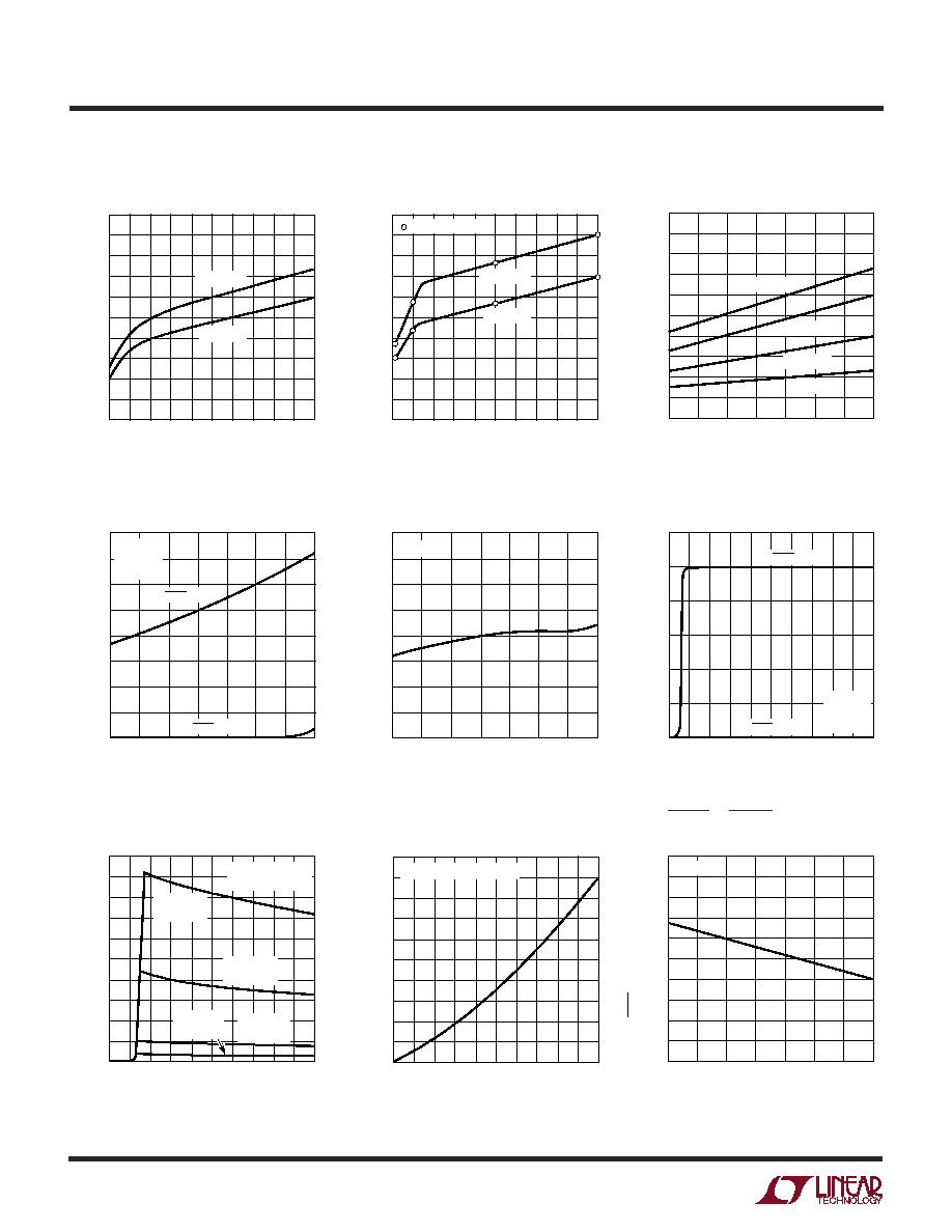
OUTPUT CURRENT (mA)
500
450
400
350
300
250
200
150
100
50
0
DROPOUT VOLTAGE (mV)
3027 G02
0
10 20 30 40
50 60 70
80 90 100
T
J
125°C
T
J
25°C
= TEST POINTS
TEMPERATURE (°C)
50
QUIESCENT CURRENT (
µ
A)
100
3027 G03
0
50
40
35
30
25
20
15
10
5
0
25
25
75
125
V
IN
= 6V
R
L
= 250k
I
L
= 5µA
V
SHDN
= V
IN
V
SHDN
= 0V
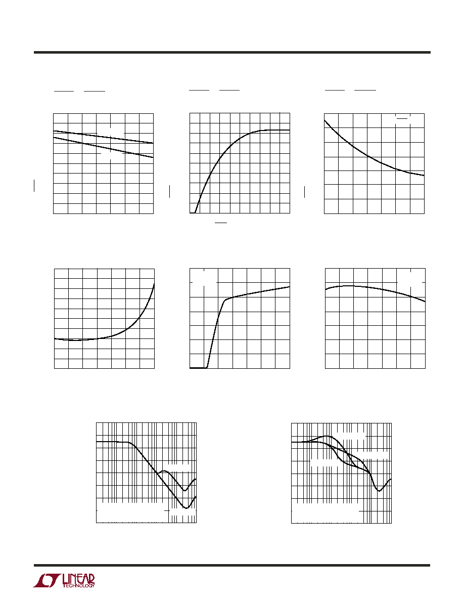
Guaranteed Dropout Voltage
Quiescent Current
Dropout Voltage
TEMPERATURE (°C)
50
DROPOUT VOLTAGE (mV)
0
50
75
3027 G03
25
25
100
125
I
L
= 100mA
I
L
= 50mA
I
L
= 10mA
I
L
= 1mA
500
450
400
350
300
250
200
150
100
50
0
OUTPUT CURRENT (mA)
500
450
400
350
300
250
200
150
100
50
0
DROPOUT VOLTAGE (mV)
3027 G01
0
10 20 30 40
50 60 70
80 90 100
T
J
= 125°C
T
J
= 25°C
Typical Dropout Voltage
TYPICAL PERFOR A CE CHARACTERISTICS
U
W
INPUT VOLTAGE (V)
0
2
6
10
14
18
QUIESCENT CURRENT (
µ
A)
30
25
20
15
10
5
0
4
8
12
16
3027 G06
20
T
J
= 25°C
R
L
= 250k
I
L
= 5µA
V
SHDN
= V
IN
V
SHDN
= 0V
Quiescent Current
ADJ1 or ADJ2 Pin Voltage
TEMPERATURE (°C)
50
ADJ PIN VOLTAGE (V)
100
3027 G05
0
50
1.240
1.235
1.230
1.225
1.220
1.215
1.210
1.205
1.200
25
25
75
125
I
L
= 1mA
INPUT VOLTAGE (V)
2.50
2.25
2.00
1.75
1.50
1.25
1.00
0.75
0.50
0.25
0
GND PIN CURRENT (mA)
3027 G07
0
1
2
3
4
5
6
7
8
9
10
T
J
= 25°C
*FOR V
OUT
= 1.22V
R
L
= 12.2
I
L
= 100mA*
R
L
= 24.4
I
L
= 50mA*
R
L
= 122
I
L
= 10mA*
R
L
= 1.22k
I
L
= 1mA*
OUTPUT CURRENT (mA)
2.50
2.25
2.00
1.75
1.50
1.25
1.00
0.75
0.50
0.25
0
GND PIN CURRENT (mA)
3027 G08
0
10 20 30 40
50 60 70
80 90 100
V
IN
= V
OUT(NOMINAL)
+ 1V
GND Pin Current
GND Pin Current vs I
LOAD
TEMPERATURE (°C)
50
SHDN PIN THRESHOLD (V)
1.0
0.9
0.8
0.7
0.6
0.5
0.4
0.3
0.2
0.1
0
0
50
75
3027 G09
25
25
100
125
I
L
= 1mA
SHDN1 or SHDN2 Pin Threshold
(On-to-Off)
5
LT3027
3027f
TYPICAL PERFOR A CE CHARACTERISTICS
U
W
SHDN1 or SHDN2 Pin Input
Current
ADJ1 or ADJ2 Pin Bias Current
Current Limit
TEMPERATURE (°C)
50
SHDN PIN INPUT CURRENT (
µ
A)
0
50
75
3027 G12
25
25
100
125
V
SHDN
= 20V
1.4
1.2
1.0
0.8
0.6
0.4
0.2
0
TEMPERATURE (°C)
50
ADJ PIN BIAS CURRENT (nA)
100
90
80
70
60
50
40
30
20
10
0
0
50
75
3027 G13
25
25
100
125
INPUT VOLTAGE (V)
0
SHORT-CIRCUIT CURRENT (mA)
2
4
5
3027 G14
1
3
6
7
350
300
250
200
150
100
50
0
V
OUT
= 0V
T
J
= 25°C
Current Limit
TEMPERATURE (°C)
50
CURRENT LIMIT (mA)
0
50
75
3027 G15
25
25
100
125
350
300
250
200
150
100
50
0
V
IN
= 7V
V
OUT
= 0V
SHDN PIN VOLTAGE (V)
1.0
0.9
0.8
0.7
0.6
0.5
0.4
0.3
0.2
0.1
0
SHDN PIN INPUT CURRENT (
µ
A)
3027 G11
0
1
2
3
4
5
6
7
8
9
10
SHDN1 or SHDN2 Pin Input
Current
TEMPERATURE (°C)
50
SHDN PIN THRESHOLD (V)
1.0
0.9
0.8
0.7
0.6
0.5
0.4
0.3
0.2
0.1
0
0
50
75
3027 G10
25
25
100
125
I
L
= 100mA
I
L
= 1mA
SHDN1 or SHDN2 Pin Threshold
(Off-to-On)
Input Ripple Rejection
FREQUENCY (kHz)
RIPPLE REJECTION (dB)
80
70
60
50
40
30
20
10
0
0.01
1
10
1000
3027 G18
0.1
100
I
L
= 100mA
V
IN
= 2.3V + 50mV
RMS
RIPPLE
C
BYP
= 0
C
OUT
= 10µF
C
OUT
= 1µF
Input Ripple Rejection
FREQUENCY (kHz)
RIPPLE REJECTION (dB)
80
70
60
50
40
30
20
10
0
0.01
1
10
1000
3027 G19
0.1
100
I
L
= 100mA
V
IN
= 2.3V + 50mV
RMS
RIPPLE
C
OUT
= 10µF
C
BYP
= 0.01µF
C
BYP
= 1000pF
C
BYP
= 100pF