 | ÐлекÑÑоннÑй компоненÑ: LT3461ES6 | СкаÑаÑÑ:  PDF PDF  ZIP ZIP |
Äîêóìåíòàöèÿ è îïèñàíèÿ www.docs.chipfind.ru
LT3461/LT3461A
1
3461af
TYPICAL APPLICATIO
U
FEATURES
DESCRIPTIO
U
APPLICATIO S
U
Digital Cameras
CCD Bias Supply
XDSL Power Supply
TFT-LCD Bias Supply
Local 5V or 12V Supply
Medical Diagnostic Equipment
Battery Backup
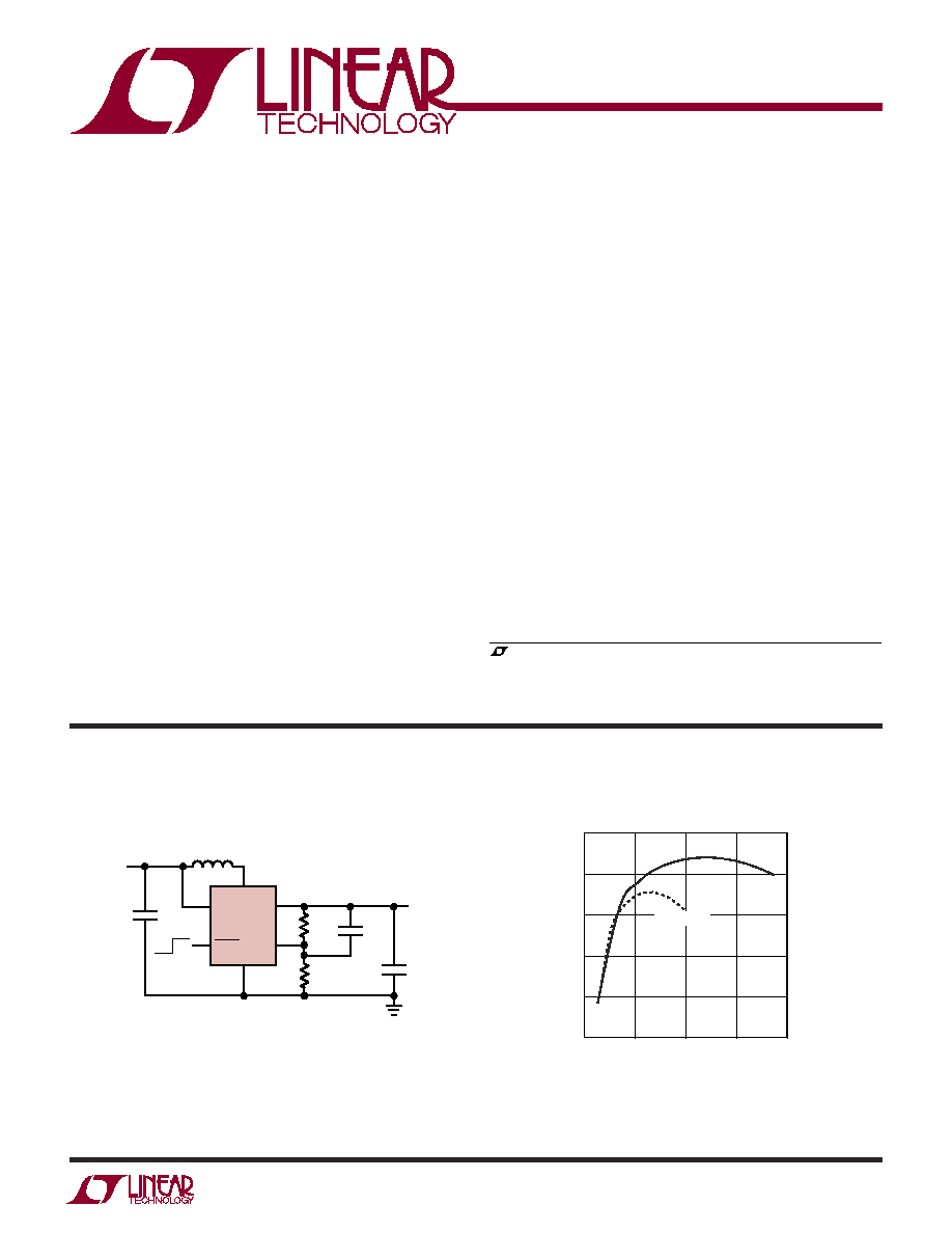
5V to 12V, 70mA Step-Up DC/DC Converter
Efficiency
V
IN
5V
L1
10µH
261k
30.1k
C2
1µF
15pF
C1
1µF
V
OUT
12V
70mA
1
2
V
IN
V
OUT
SW
3
4
5
6
FB
SHDN
GND
LT3461A
3461 TA01a
OFF ON
Integrated Schottky Rectifier
Fixed Frequency 1.3MHz/3MHz Operation
High Output Voltage: Up to 38V
Low V
CESAT
Switch: 260mV at 250mA
12V at 70mA from 5V Input
5V at 115mA from 3.3V Input
Wide Input Range: 2.5V to 16V
Uses Small Surface Mount Components
Low Shutdown Current: <1µA
Soft-Start
Low Profile (1mm) SOT-23 (ThinSOT
TM
) Package
1.3MHz/3MHz Step-Up
DC/DC Converters with
Integrated Schottky in ThinSOT
The LT
®
3461/LT3461A are general purpose fixed fre-
quency current mode step-up DC/DC converters. Both
devices feature an integrated Schottky and a low V
CESAT
switch allowing a small converter footprint and lower parts
cost. The LT3461 switches at 1.3MHz while the LT3461A
switches at 3MHz. These high switching frequencies en-
able the use of tiny, low cost and low height capacitors and
inductors. The constant switching frequency results in
predictable output noise that is easy to filter, and the
inductor based topology ensures an input free from switch-
ing noise typically present with charge pump solutions.
The high voltage switch in the LT3461/LT3461A is rated at
40V making the device ideal for boost converters up to
38V.
The LT3461/LT3461A are available in a low profile (1mm)
SOT-23 package.
, LTC and LT are registered trademarks of Linear Technology Corporation.
ThinSOT is a trademark of Linear Technology Corporation.
LOAD CURRENT (mA)
0
EFFICIENCY (%)
85
80
75
70
65
60
3461 TAO1b
20
40
60
80
V
IN
= 5V
V
IN
= 3.3V
LT3461/LT3461A
2
3461af
PARAMETER
CONDITIONS
MIN
TYP
MAX
UNITS
Minimum Operating Voltage
2.5
V
Maximum Operating Voltage
16
V
Feedback Voltage
1.235
1.255
1.275
V
1.225
1.280
V
Feedback Line Regulation
0.005
%/V
FB Pin Bias Current
40
100
nA
Supply Current
FB = 1.3V, Not Switching
2.8
3.6
mA
SHDN = 0V
0.1
0.5
µA
Switching Frequency (LT3461A)
2.1
3.0
3.9
MHz
Switching Frequency (LT3461)
1.0
1.3
1.7
MHz
Maximum Duty Cycle (LT3461A)
82
%
Maximum Duty Cycle (LT3461)
92
%
Switch Current Limit
300
420
600
mA
Switch V
CESAT
I
SW
= 250mA
260
350
mV
Switch Leakage Current
V
SW
= 5V
0.01
1
µA
Schottky Forward Voltage
I
SCHOTTKY
= 250mA
800
1100
mV
Schottky Reverse Leakage
V
OUT
SW = 40V
0.03
4
µA
SHDN Voltage High
1.5
V
SHDN Voltage Low
0.4
V
SHDN Pin Bias Current
35
50
µA
Input Voltage (V
IN
) .................................................. 16V
V
OUT
, SW Voltage .................................................... 40V
FB Voltage ................................................................. 5V
SHDN Voltage .......................................................... 16V
Operating Ambient
Temperature Range (Note 2) .................. 40°C to 85°C
Maximum Junction Temperature .......................... 125°C
Storage Temperature Range ................. 65°C to 150°C
Lead Temperature (Soldering, 10 sec).................. 300°C
ABSOLUTE AXI U
RATI GS
W
W
W
U
PACKAGE/ORDER I FOR ATIO
U
U
W
(Note 1)
ELECTRICAL CHARACTERISTICS
The
denotes the specifications which apply over the full operating
temperature range, otherwise specifications are at T
A
= 25°C, V
IN
= 3V, V
SHDN
= 3V, unless otherwise noted.
Consult LTC Marketing for parts specified with wider operating temperature ranges.
ORDER PART
NUMBER
S6 PART MARKING
LTAHG
LTAEB
LT3461AES6
LT3461ES6
T
JMAX
= 125°C,
JA
= 150°C ON BOARD OVER
GROUND PLANE,
JC
= 120°C/W
Note 1: Absolute Maximum Ratings are those values beyond which the life
of a device may be impaired.
Note 2: The LT3461E/LT3461AE is guaranteed to meet specifications from
0°C to 70°C. Specifications over the 40°C to 85°C operating temperature
range are assured by design, characterization and correlation with
statistical process controls.
6 V
IN
5 V
OUT
4 SHDN
SW 1
TOP VIEW
S6 PACKAGE
6-LEAD PLASTIC TSOT-23
GND 2
FB 3
LT3461/LT3461A
3
3461af
TEMPERATURE (°C)
FB VOLTAGE (V)
1.28
1.27
1.26
1.25
1.24
1.23
1.22
3461a G03
DUTY CYCLE (%)
10
CURRENT LIMIT (mA)
90
80
60
40
20
3461a G02
30
50
70
480
360
240
120
0
3461a G06
TEMPERATURE (°C)
60 40
FREQUENCY (MHz)
3.9
3.6
3.3
3.0
2.7
2.4
2.1
20
60
3461a G04
20
0
40
80
100
SHDN PIN VOLTAGE (V)
1.3
CURRENT LIMIT (mA)
1.9
2.3
3461a G05
1.5
1.7
2.1
480
420
360
300
240
180
120
60
0
T
A
= 25°C
T
A
= 25°C
SHDN PIN VOLTAGE (V)
0
SHDN PIN CURRENT (
µ
A)
16
4
8
12
320
280
240
200
160
120
80
40
0
T
A
= 25°C
40
20
60
20
0
40
80
100
TEMPERATURE (°C)
FREQUENCY (MHz)
1.6
1.5
1.4
1.3
1.2
1.1
1.0
3461a G01
40
20
60
20
0
40
80
100
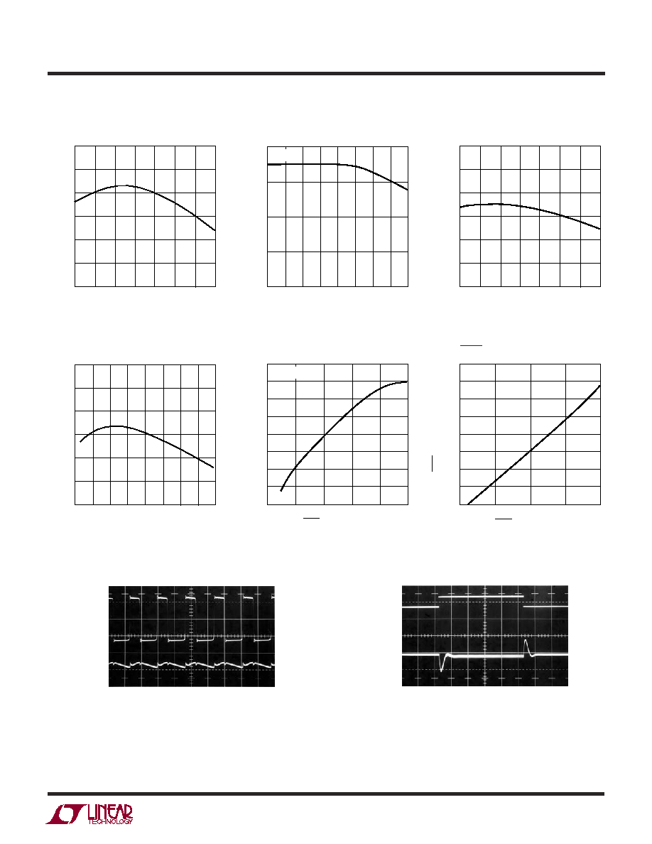
TYPICAL PERFOR A CE CHARACTERISTICS
U
W
Oscillator Frequency (LT3461A)
Current Limit
FB Pin Voltage
Current Limit in Soft-Start Mode
V
SW
5V/DIV
V
OUT
50mV/DIV
0.2µs/DIV
3461a G08
I
LOAD
= 60mA
70mA
V
OUT
100mV/DIV
50µs/DIV
3461a G09
I
LOAD
35mA
Switching Waveform
Circuit of Figure 4
Load Transient Response
Circuit of Figure 4
SHDN Pin Current
Oscillator Frequency (LT3461)
LT3461/LT3461A
4
3461af
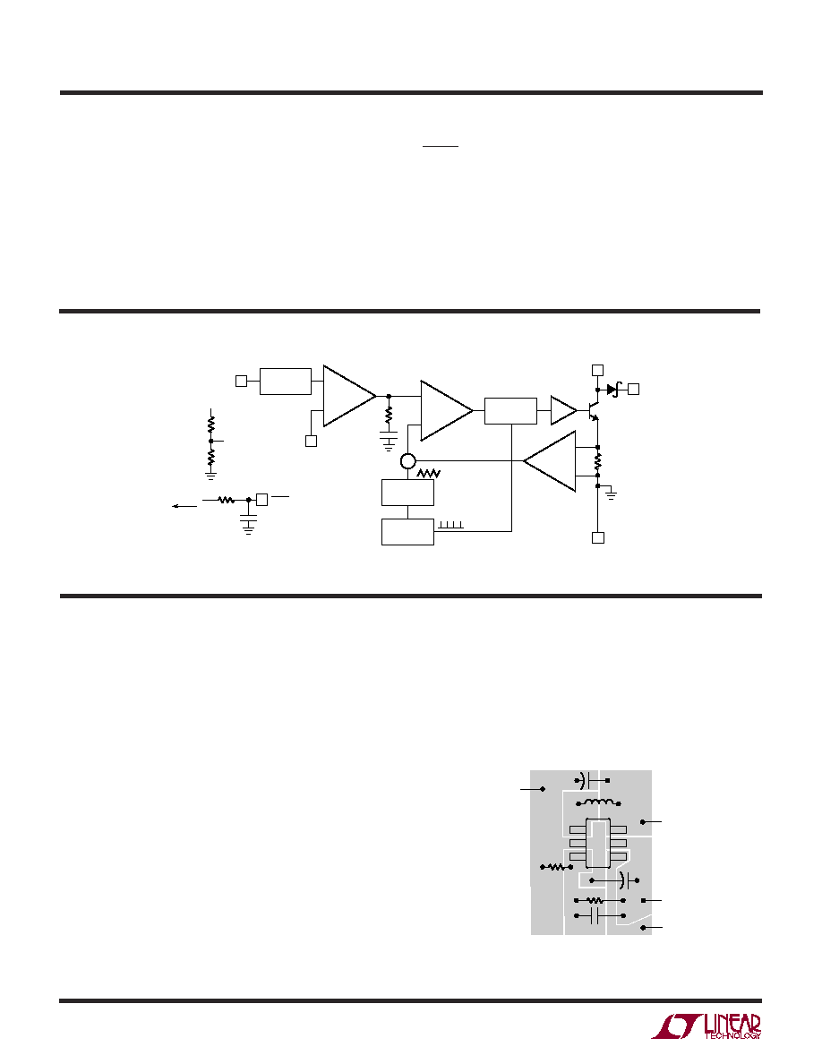
OPERATIO
U
Figure 2. Suggested Layout
R2
R1
GND
C3
L1
C1
V
OUT
V
IN
SHUTDOWN
+
C2
+
3461a F03
The LT3461/LT3461A uses a constant frequency, current
mode control scheme to provide excellent line and load
regulation. Operation can be best understood by referring
to the block diagram in Figure 1. At the start of each
oscillator cycle, the SR latch is set, which turns on the
power switch Q1. A voltage proportional to the switch
current is added to a stabilizing ramp and the resulting
sum is fed into the positive terminal of the PWM compara-
tor A2. When this voltage exceeds the level at the negative
input of A2, the SR latch is reset turning off the power
switch. The level at the negative input of A2 is set by the
error amplifier A1, and is simply an amplified version of
the difference between the feedback voltage and the
reference voltage of 1.255V. In this manner, the error
amplifier sets the correct peak current level to keep the
output in regulation. If the error amplifier's output in-
creases, more current is delivered to the output; if it
decreases, less current is delivered.
Layout Hints
The high speed operation of the LT3461/LT3461A de-
mands careful attention to board layout. You will not get
advertised performance with careless layout. Figure 2
shows the recommended component placement.
BLOCK DIAGRA
W
+
+
+
6
1
3
2
V
OUT
V
OUT
R1 (EXTERNAL)
R2 (EXTERNAL)
R
S
(EXTERNAL)
C
S
(EXTERNAL)
FB
SHUTDOWN
SHDN
RAMP
GENERATOR
1.255V
REFERENCE
3MHz*
OSCILLATOR
R
S
Q
4
A1
A2
COMPARATOR
DRIVER
R
C
C
C
SW
Q1
0.1
GND
V
IN
FB
3461a F02
R
S
, C
S
OPTIONAL SOFT-START COMPONENTS
5
*LT3461 IS 1.3MHz
Figure 1. Block Diagram
U
U
U
PI FU CTIO S
SW (Pin 1): Switch Pin. Connect inductor here. Minimize
trace at this pin to reduce EMI.
GND (Pin 2): Ground Pin. Tie directly to local ground
plane.
FB (Pin 3): Feedback Pin. Reference voltage is 1.255V.
Connect resistor divider tap here. Minimize trace area at
FB. Set V
OUT
according to V
OUT
= 1.255V (1 + R1/R2).
SHDN (Pin 4): Shutdown Pin. Tie to 1.5V or higher to
enable device; 0.4V or less to disable device. Also func-
tions as soft-start. Use RC filter (47k, 47nF typ) as shown
in Figure 1.
V
OUT
(Pin 5): Output Pin. Connect to resistor divider. Put
capacitor close to pin and close to GND plane.
V
IN
(Pin 6): Input Supply Pin. Must be locally bypassed.
LT3461/LT3461A
5
3461af
Inrush Current
The LT3461 has a built-in Schottky diode. When supply
voltage is applied to the V
IN
pin, the voltage difference
between V
IN
and V
OUT
generates inrush current flowing
from input through the inductor and the Schottky diode to
charge the output capacitor. The maximum nonrepetitive
surge current the Schottky diode in the LT3461 can
sustain is 1.5A. The selection of inductor and capacitor
value should ensure the peak of the inrush current to be
below 1.5A. In addition, turn-on of the LT3461 should be
delayed until the inrush current is less than the maximum
current limit. The peak inrush current can be calculated as
follows:
I
V
L
C
L
C
P
IN
=
-
-
.
· exp
0 6
1
2
1
where L is the inductance, r is the resistance of the
inductor and C is the output capacitance.
Table 3 gives inrush peak currents for some component
selections.
Table 3. Inrush Peak Current
V
IN
(V)
L (µH)
C (µF)
I
P
(A)
5
4.7
1
1.1
5
10
1
0.9
Thermal Considerations
Significant power dissipation can occur on the LT3461
and LT3461A, particularly at high input voltage. Device
load, voltage drops in the power path components, and
switching losses are the major contributors. It is impor-
tant to measure device power dissipation in an application
to ensure that the LT3461 does not exceed the absolute
maximum operating junction temperature of 125°C over
the operating ambient temperature range. Generally, for
supply voltages below 5V the integrated current limit
function provides adequate protection for nonfault condi-
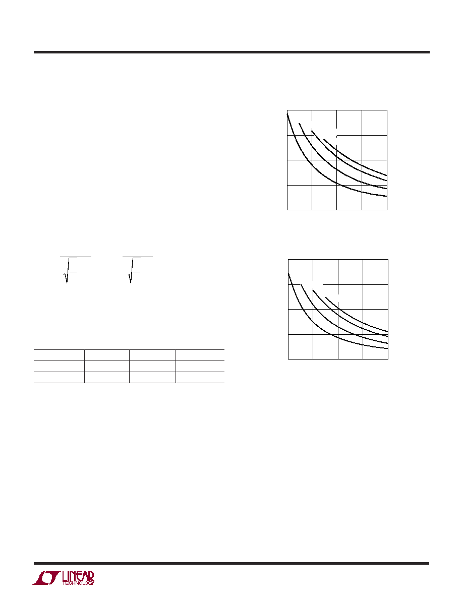
tions. For supply voltages above 5V, Figures 3a and 3b
show the recommended operating region of the LT3461
and LT3461A, respectively. These graphs are based
on 250mW on-chip dissipation. Improvement of these
APPLICATIO S I FOR ATIO
W
U
U
U
numbers can be expected if the LT3461 is supplied from a
separate low voltage rail.
Figure 3a. LT3461 Operating Region
Figure 3b. LT3461A Operating Region
V
OUT
(V)
6
I
OUT
(mA)
80
120
38
3461 F01a
40
0
14
22
30
160
V
IN
>15V
V
IN
= 12V
V
IN
= 8V
V
IN
= 5V
V
OUT
(V)
6
I
OUT
(mA)
80
120
38
3461 F01b
40
0
14
22
30
160
V
IN
>15V
V
IN
= 12V
V
IN
= 8V
V
IN
= 5V
Switching Frequency
The key difference between the LT3461 and LT3461A is the
faster switching frequency of the LT3461A. At 3MHz, the
LT3461A switches at twice the rate of the LT3461. The
higher switching frequency of the LT3461A allows physi-
cally smaller inductors and capacitors to be used in a given
application, but with a slight decrease in efficiency and
maximum output current when compared to the LT3461.
Generally if efficiency and maximum output current are
crucial, or a high output voltage is being generated, the
LT3461 should be used. If application size and cost are
more important, the LT3461A will be the better choice.
LT3461/LT3461A
6
3461af
Inductor Selection
The inductors used with the LT3461/LT3461A should
have a saturation current rating of 0.3A or greater. If the
device is used in an application where the input supply will
be hot-plugged, then the saturation current rating should
be equal to or greater than the peak inrush current. For the
LT3461, an inductor value between 10µH and 47µH,
depending upon output voltage, will usually be the best
choice for most designs. For the LT3461A, inductor values
between 4.7µH and 15µH inductor will suffice for most
applications. For best loop stability results, the inductor
value selected should provide a ripple current of 70mA or
more. For a given V
IN
and V
OUT
the inductor value to use
with LT3461A is estimated by the formula:
L (in microhenries) =
D V
V
A
V
IN
OUT
·
·
· sec
·
1
1
1
where D
=
+
+
V
V
V
V
V
OUT
IN
OUT
1
1
Use twice this value for the LT3461.
Capacitor Selection
Low ESR capacitors should be used at the output to
minimize the output voltage ripple. Multilayer ceramic
capacitors using X5R/X7R dielectrics are preferred as they
have a low ESR and maintain capacitance over wide
voltage and temperature range. A 2.2µF output capacitor
is sufficient for most applications using the LT3461, while
a 1µF capacitor is sufficient for most applications using
the LT3461A. High output voltages typically require less
capacitance for loop stability. Always use a capacitor with
sufficient voltage rating.
Either ceramic or solid tantalum capacitors may be used
for the input decoupling capacitor, which should be placed
as close as possible to the LT3461/LT3461A. A 1µF
capacitor is sufficient for most applications.
Phase Lead Capacitor
A small value capacitor can be added across resistor R1
between the output and the FB pin to reduce output
perturbation due to a load step and to improve transient
response. This phase lead capacitor introduces a pole-
zero pair to the feedback that boosts phase margin near
the cross-over frequency. The following formula is useful
to estimate the capacitor value needed:
C
k
R
pF
PL
=
500
2
1
·
For an application running 50µA in the feedback divider,
capacitor values from 10pF to 22pF work well.
APPLICATIO S I FOR ATIO
W
U
U
U
TYPICAL APPLICATIO S
U
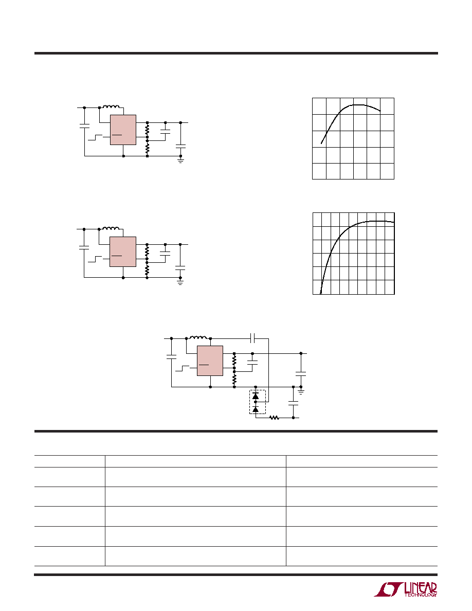
Figure 4. 5V to 12V with Soft-Start Circuit (LT3461A)
Input Current and Output Voltage
V
IN
5V
L1
10µH
R1
261k
R2
30.1k
C2
1µF
15pF
C1
1µF
V
OUT
12V
70mA
1
2
V
IN
V
OUT
SW
3
4
5
6
FB
SHDN
GND
LT3461A
3461a TA02a
CONTROL
SIGNAL
47nF
47k
C1, C2: TAIYO YUDEN EMK212BJ105
L1: MURATA LQH32CN100K53
I
IN
50mA/DIV
CONTROL
SIGNAL
5V/DIV
1ms/DIV
V
OUT
5V/DIV
3461a TA02b
LT3461/LT3461A
7
3461af
3.3V to 5V Step-Up Converter (LT3461A)
3.3V to 5V Step-Up Converter Efficiency
V
IN
3.3V
L1
4.7µH
R1
45.3k
R2
15k
C2
1µF
15pF
C1
1µF
V
OUT
5V
115mA
1
2
V
IN
V
OUT
SW
3
4
5
6
FB
SHDN
GND
LT3461A
C1, C2: TAIYO YUDEN X7R LMK212BJ105
L1: MURATA LQH32CN4R7M33 OR EQUIVALENT
3461a TA03a
OFF ON
LOAD CURRENT (mA)
0
EFFICIENCY (%)
80
75
70
65
60
3461a TA03b
60
30
120
90
TYPICAL APPLICATIO S
U
Information furnished by Linear Technology Corporation is believed to be accurate and reliable.
However, no responsibility is assumed for its use. Linear Technology Corporation makes no represen-
tation that the interconnection of its circuits as described herein will not infringe on existing patent rights.
PACKAGE DESCRIPTIO
U
S6 Package
6-Lead Plastic TSOT-23
(Reference LTC DWG # 05-08-1636)
1.50 1.75
(NOTE 4)
2.80 BSC
0.30 0.45
6 PLCS (NOTE 3)
DATUM `A'
0.09 0.20
(NOTE 3)
S6 TSOT-23 0302
2.90 BSC
(NOTE 4)
0.95 BSC
1.90 BSC
0.80 0.90
1.00 MAX
0.01 0.10
0.20 BSC
0.30 0.50 REF
PIN ONE ID
NOTE:
1. DIMENSIONS ARE IN MILLIMETERS
2. DRAWING NOT TO SCALE
3. DIMENSIONS ARE INCLUSIVE OF PLATING
4. DIMENSIONS ARE EXCLUSIVE OF MOLD
FLASH AND METAL BURR
5. MOLD FLASH SHALL NOT EXCEED 0.254mm
6. JEDEC PACKAGE REFERENCE IS MO-193
3.85 MAX
0.62
MAX
0.95
REF
RECOMMENDED SOLDER PAD LAYOUT
PER IPC CALCULATOR
1.4 MIN
2.62 REF
1.22 REF
LT3461/LT3461A
8
3461af
Linear Technology Corporation
1630 McCarthy Blvd., Milpitas, CA 95035-7417
(408) 432-1900
FAX: (408) 434-0507
www.linear.com
© LINEAR TECHNOLOGY CORPORATION 2003
LT/TP 1004 1K · PRINTED IN USA
RELATED PARTS
PART NUMBER
DESCRIPTION
COMMENTS
LT1615/LT1615-1
300mA/80mA (I
SW
) Constant Off-Time,
V
IN
: 1.2V to 15V, V
OUT(MAX)
= 34V, I
Q
= 20µA,
High Efficiency Step-Up DC/DC Converter
I
SD
<1µA, ThinSOT Package
LT1944/LT1944-1
Dual Output 350mA/100mA (I
SW
), Constant Off-Time,
V
IN
: 1.2V to 15V, V
OUT(MAX)
= 34V, I
Q
= 20µA,
High Efficiency Step-Up DC/DC Converter
I
SD
<1µA, MS Package
LTC3400/LTC3400B
600mA (I
SW
), 1.2MHz, Synchronous Step-Up DC/DC Converter
V
IN
: 0.85V to 5V, V
OUT(MAX)
= 5V, I
Q
= 19µA/300µA,
I
SD
<1µA, ThinSOT
LT3460
0.32A (I
SW
), 1.3MHz, High Efficiency Step-Up DC/DC Converter
V
IN
: 2.5V to 16V, V
OUT(MAX)
= 36V, I
Q
= 2mA,
I
SD
<1µA, SC70, ThinSOT Packages
LT3465/LT3465A
Constant Current, 1.2MHz/2.7MHz, High Efficiency White LED
V
IN
: 2.7V to 16V, V
OUT(MAX)
= 34V, I
Q
= 1.9mA,
Boost Regulator with Integrated Schottky Diode
I
SD
<1µA, ThinSOT Package
TYPICAL APPLICATIO S
U
Low Profile (1mm) 3.3V to 15V Step-Up Converter
3.3V to 15V Efficiency
V
IN
3.3V
L1
10µH
332k
30.1k
C2
2.2µF
22pF
C1
1µF
V
OUT
15V
25mA
1
2
V
IN
V
OUT
SW
3
4
5
6
FB
SHDN
GND
LT3461A
C1: TAIYO YUDEN LMK107BJ105KA
C2: TAIYO YUDEN EMK316BJ225KD (X5R)
L1: MURATA LQH2MCN100K02
3461a TA04a
OFF ON
LOAD CURRENT (mA)
0
EFFICIENCY (%)
75
70
65
60
55
50
3461a TA04b
10
5
20
30
15
25
V
IN
5V
L1
47µH
280k
10k
C2
0.47µF
50V
22pF
C1
1µF
V
OUT
36V
18mA
1
2
V
IN
V
OUT
SW
3
4
5
6
FB
SHDN
GND
LT3461
C1: TAIYO YUDEN X7R LMK212BJ105
C2: MURATA GRM42-6X7R474K50
L1: MURATA LQH32CN470
3461 TA05a
OFF ON
LOAD CURRENT (mA)
0
EFFICIENCY (%)
16
3461 TA05b
8
12
14
6
2
4
10
80
75
70
65
60
55
50
18
5V to 36V Step-Up Converter (LT3461)
5V to 36V Efficiency
3.3V to ±5V Dual Output Converter
V
IN
3.3V
L1
4.7µH
45.3k
15k
15pF
C1
1µF
1
2
V
IN
V
OUT
SW
3
4
5
6
FB
SHDN
GND
LT3461A
OFF ON
3461 TA06
C4
1µF
C2
1µF
C3
1µF
5V
15mA
D1
D2
V
OUT
5V
100mA
C1, C2, C3, C4: TAIYO YUDEN JMK107BJ105
D1, D2: PHILIPS PMEG2005EB
L1: MURATA LQH2MCN4R7M02
10