 | –≠–ª–µ–∫—Ç—Ä–æ–Ω–Ω—ã–π –∫–æ–º–ø–æ–Ω–µ–Ω—Ç: LT3479 | –°–∫–∞—á–∞—Ç—å:  PDF PDF  ZIP ZIP |
1
LTC3490
3490f
Portable Lighting
Rechargeable Flashlights
Single Cell Minimum Component LED Driver
Single Cell 350mA
LED Driver
350mA Constant Current Output
2.8V to 4V Output Compliance
1- or 2-Cell NiMH or Alkaline Input
Synchronous Rectification: Up to 90% Efficiency
Fixed Frequency Operation: 1.3MHz
Low Quiescient Current: <1mA
Very Low Shutdown Current: <50
µA
Open LED Output Limited to 4.7V
V
IN
Range: 1V to 3.2V
Dimming Control
Undervoltage Lockout to Protect Batteries
Low Profile (0.75mm) 3mm
◊ 3mm Thermally
Enhanced 8-Lead DD and S8 Packages
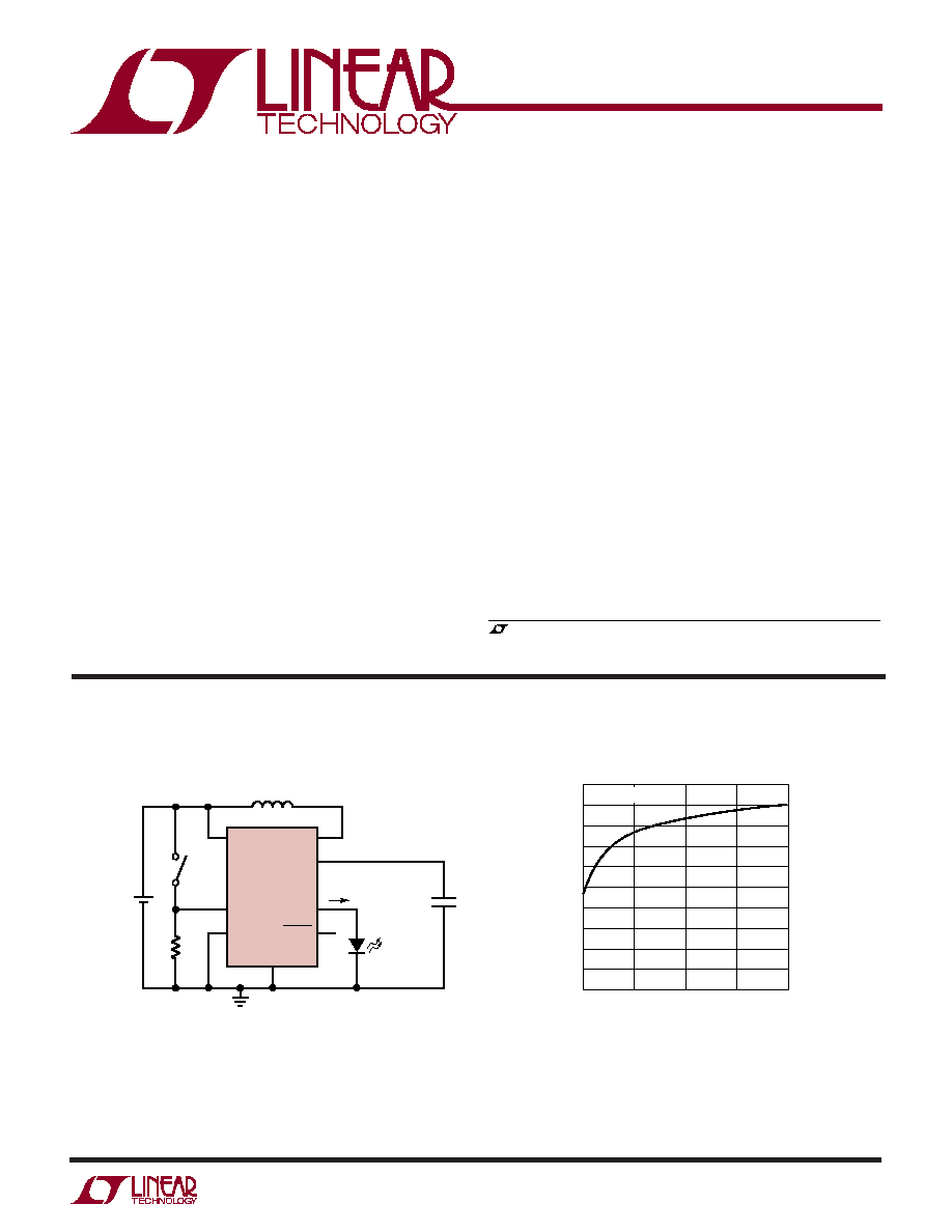
Efficiency vs V
IN
at V
LED
= 3.5V
FEATURES
DESCRIPTIO
U
APPLICATIO S
U
TYPICAL APPLICATIO
U
The LTC
Æ
3490 provides a constant current drive for 1W
LED applications. It is a high efficiency boost converter
that operates from 1 or 2 NiMH or alkaline cells and
generates 350mA of constant current with up to 4V of
compliance. It contains a 100m
NFET switch and a
130m
PFET synchronous rectifier. The fixed switching
frequency is internally set to 1.3MHz.
The LTC3490 limits the output voltage to 4.7V if the output
load is disconnected. It also features an analog dimming
capability that reduces the drive current proportional to
the CTRL/SHDN pin voltage. A low-battery logic output
signals when the battery has dropped below 1V/cell. An
undervoltage lockout circuit shuts down the LTC3490
when the battery voltage drops below 0.85V/cell. The
feedback loop is internally compensated to minimize com-
ponent count.
+
SW
CAP
ON/OFF
LED
1 NiMH OR
ALKALINE
CELL
4.7
µF
LOBAT
3490 TA01
V
IN
CTRL/SHDN
CELLS
1M
HIGH
CURRENT
LED
GND
LTC3490
3.3
µH
350mA
V
IN
(V)
1
0
EFFICIENCY (%)
10
30
40
50
100
70
1.5
2
3490 TA02
20
80
90
60
2.5
3
I
OUT
= 350mA
, LTC and LT are registered trademarks of Linear Technology Corporation.
All other trademarks are the property of their respective owners.
2
LTC3490
3490f
Supply Voltage (V
IN
) ................................... ≠ 0.3V to 6V
Input Voltages (CTRL/SHDN, CELLS) ......... ≠ 0.3V to 6V
Output Voltages (CAP, LED, SW) ................ ≠ 0.3V to 6V
Consult LTC Marketing for parts specified with wider operating temperature ranges.
ABSOLUTE AXI U RATI GS
W
W
W
U
PACKAGE/ORDER I FOR ATIO
U
U
W
(Note 1)
LTC3490EDD
ORDER PART
NUMBER
DD PART MARKING
LBRQ
T
JMAX
= 125
∞C,
JA
= 43
∞C/ W (NOTE 4)
EXPOSED PAD (PIN 9) IS GND
MUST BE SOLDERED TO PCB (NOTE 5)
Operating Temperature Range (Note 2) .. ≠ 40
∞C to 85∞C
Storage Temperature Range ................. ≠ 65
∞C to 125∞C
Lead Temperature (Soldering, 10 sec, S8) .......... 300
∞C
LTC3490ES8
ORDER PART
NUMBER
S8 PART MARKING
3490
T
JMAX
= 125
∞C,
JA
= 150
∞C/ W (NOTE 4)
TOP VIEW
9
DD PACKAGE
8-LEAD (3mm
◊ 3mm) PLASTIC DFN
5
6
7
8
4
3
2
1
CELLS
V
IN
SW
GND
CTRL/SHDN
LOBAT
CAP
LED
1
2
3
4
8
7
6
5
TOP VIEW
CTRL/SHDN
LOBAT
CAP
LED
CELLS
V
IN
SW
GND
S8 PACKAGE
8-LEAD PLASTIC SO
SYMBOL
PARAMETER
CONDITIONS
MIN
TYP
MAX
UNITS
V
IN
Input Supply Range
1
3.2
V
V
IN(START)
Minimum Start-Up Voltage
(Note 3)
0.9
1
V
I
LED(MAX)
LED Drive Current
V
CTRL/SHDN
= V
IN
, DD Package
25
∞C to 85∞C
330
350
370
mA
≠ 40
∞C to <25∞C
310
350
385
mA
V
CTRL/SHDN
= V
IN
, S8 Package
25
∞C to 85∞C
337
350
363
mA
≠ 40
∞C to <25∞C
325
345
365
mA
I
LED(SHDN)
LED Drive Current in Shutdown
V
CTRL/SHDN
= 0V
0.1
1
µA
V
LED
Output Compliance Voltage
2.8
4
V
V
LED(OVL)
Output Voltage Overvoltage Limit
Open LED
4.2
4.7
V
I
IN(SHDN)
Input Current, Shutdown
V
CTRL/SHDN
= 0V, Excluding Switch Leakage
20
50
µA
I
IN(ACTIVE)
Input Current, Active
Excluding Load Power
20
30
mA
f
SW
Switching Frequency
1.0
1.3
1.6
MHz
I
L(NMOS)
Leakage Current, NMOS Switch
0.1
µA
R
ON(NMOS)
On Resistance, NMOS Switch
0.1
I
L(PMOS)
Leakage Current, PMOS Switch
0.1
µA
R
ON(PMOS)
On Resistance, PMOS Switch
0.13
V
IH
Input High (CELLS)
V
IN
≠ 0.4
V
Input High (SHDN)
V
IN
∑ 0.9
V
V
IL
Input Low (CELLS)
0.4
V
Input Low (SHDN)
V
IN
∑ 0.2
V
The
denotes specifications which apply over the full operating
temperature range, otherwise specifications are T
A
= 25
∞C. V
IN
= 2.5V unless otherwise specified.
ELECTRICAL CHARACTERISTICS
3
LTC3490
3490f
SYMBOL
PARAMETER
CONDITIONS
MIN
TYP
MAX
UNITS
The
denotes specifications which apply over the full operating
temperature range, otherwise specifications are T
A
= 25
∞C. V
IN
= 2.5V unless otherwise specified.
ELECTRICAL CHARACTERISTICS
I
IN
Input Current (CTRL/SHDN, CELLS)
0.01
µA
K
CTRL
Control Gain, I
LED
/V
CTRL
Scales Linearity with V
IN
, V
IN
= 1V
500
mA/V
R
ON(LOBAT)
On Resistance, LOBAT Output
V
IN
Below UVLO Threshold
300
V
IN(LOBAT1)
Input Voltage, Low Battery, 1 Cell
V
CELLS
= 0V
0.8
1.12
V
V
IN(LOBAT2)
Input Voltage, Low Battery, 2 Cells
V
CELLS
= V
IN
1.8
2.24
V
V
IN(UVLO2)
Input Voltage, Undervoltage Lockout, V
CELLS
= V
IN
1.4
1.8
V
2 Cells
V
IN(UVLO1)
Input Voltage, Undervoltage Lockout, V
CELLS
= 0 V
0.7
0.9
V
1 Cell
Note 1: Absolute Maximum Ratings are those values beyond which the life
of a device may be impaired.
Note 2: The LTC3490 is guaranteed to meet performance specifications
from 0
∞C to 70∞C. Specifications over the ≠40∞C to 85∞C range are
assured by design, characterization and correlation with statistical process
controls.
Note 3: The LTC3490 input voltage may drop below the minimum start-up
voltage once the LED voltage has risen above 2.3V.
Note 4: This device includes overtemperature protection intended to
protect the device during momentary overload conditions. The maximum
junction temperature may be exceeded when overtemperature protection
is active. Continuous operation above the specified maximum operating
junction temperature may result in device degradation or failure.
Note 5: The Exposed Pad of the DFN package must be soldered to a PCB
pad for optimum thermal conductivity. This pad must be connected to
ground.
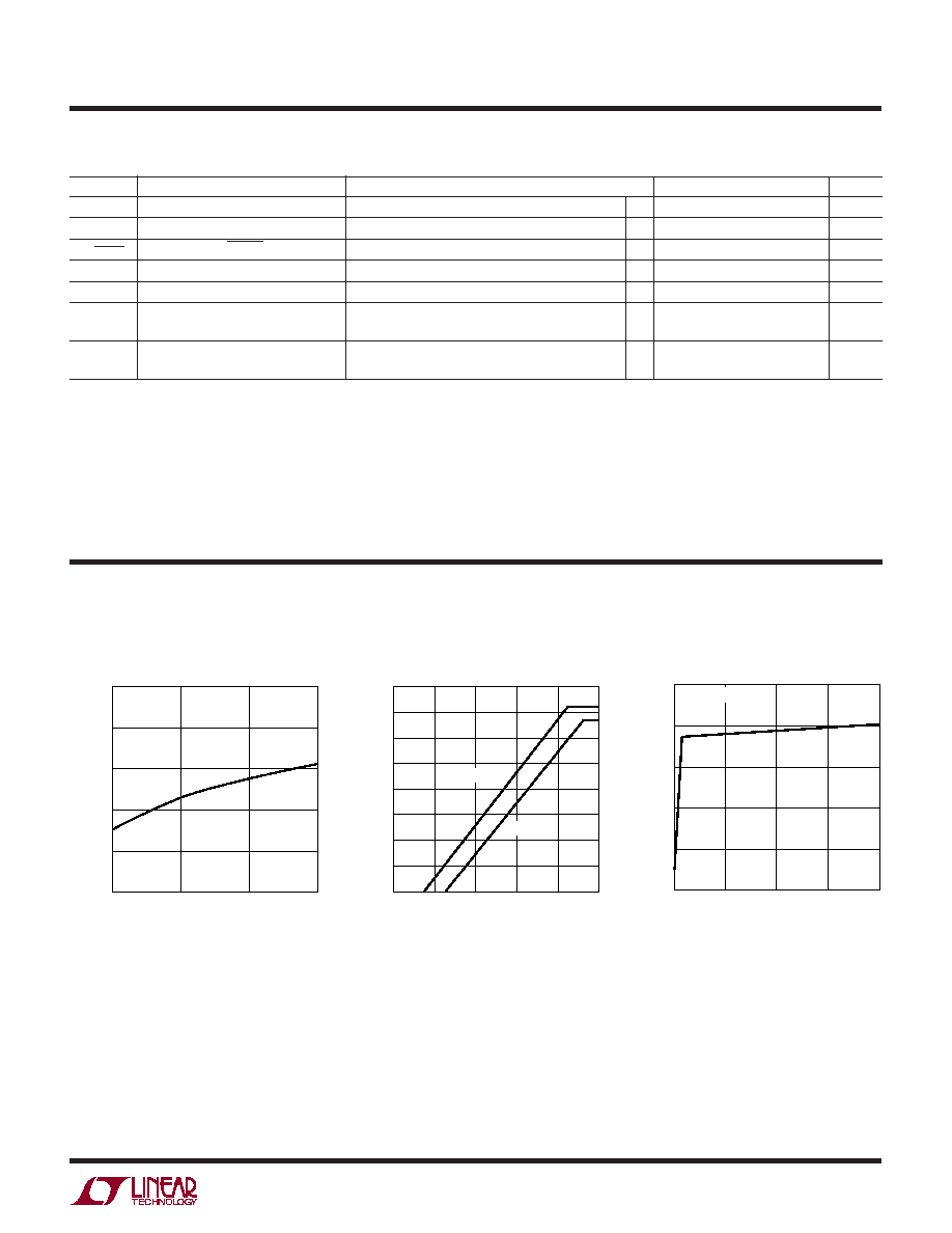
TYPICAL PERFOR A CE CHARACTERISTICS
U
W
Oscillator Frequency
vs Temperature
I
LED
vs V
CTRL
V
CTRL
/V
IN
(V)
0
I
LED
(mA)
150
200
250
0.6
1
3490 G02
100
50
0
0.2
0.4
0.8
300
350
400
MAXIMUM
MINIMUM
I
LED
vs V
IN
V
IN
(V)
I
LED
(mA)
325
350
375
2.5
3490 G03
300
275
250
1
1.5
2
3
V
LED
= 3.5V
TEMPERATURE (
∞C)
≠50
FREQUENCY (MHz)
1.280
1.320
3490 G01
1.240
1.200
0
50
100
1.400
1.360
4
LTC3490
3490f
U
U
U
PI FU CTIO S
CELLS (Pin 1): A logic input to set the low-battery and
undervoltage shutdown thresholds. A logic low (tied to
GND) will set the thresholds for 1 cell. A logic high (tied to
V
IN
) will set the thresholds for 2 cells.
V
IN
(Pin 2): Supply Voltage.
SW (Pin 3): Switch Input. Connect this pin to an external
inductor from V
IN
.
GND (Pin 4): Circuit Ground.
LED (Pin 5): Output Drive Current to LED.
CAP (Pin 6): Filter Capacitor. A 4.7
µF low ESR capacitor
should be tied to this pin.
LOBAT (Pin 7): Low active, open-drain logic output indi-
cating a low-battery condition.
CTRL/SHDN (Pin 8): Analog Control Voltage and Shut-
down. When V
IN
∑ 0.2 < V
CTRL
< V
IN
∑ 0.9, the LED drive
current varies according to the formula:
I
V
V
mA
LED
CTRL
IN
=
500
0 2
∑
≠ .
When V
CTRL
> V
IN
∑ 0.9, the LED drive current is clamped
at 350mA. When V
CTRL
< V
IN
∑ 0.2, then the part is in low
power shutdown.
Exposed Pad (Pin 9, DD Package): Ground. This pin must
be soldered to the PCB to provide both electrical contact
to ground and good thermal contact to the PCB.
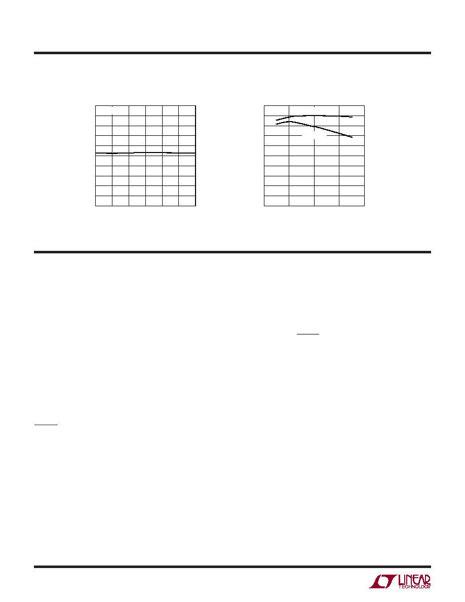
I
LED
vs V
LED
V
LED
(V)
2.8
340
I
LED
(mA)
342
346
348
350
360
354
3
3.2
3.4
3.6
3.8
3490 G04
344
356
358
352
4
V
IN
= 2.4V
TYPICAL PERFOR A CE CHARACTERISTICS
U
W
I
LED
(mA)
0
0
EFFICIENCY (%)
10
30
40
50
100
70
100
200
3490 G05
20
80
90
60
300
400
V
IN
= 2.4V
V
IN
= 1.2V
Efficiency vs I
LED
5
LTC3490
3490f
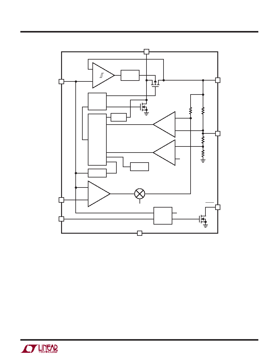
FU CTIO AL DIAGRA
U
U
W
≠
+
2
3
6
SW
CAP
GATE
CONTROL
AND
DRIVERS
BATTERY
MONITOR
PWM
LOGIC
LIMIT
V
IN
8
CTRL/
SHDN
START-UP
OSCILLATOR
I
REF
SENSE
AMP
OVERVOLTAGE
DETECT
DIMMING
AMP
19.2
0.1
250k
40k
V
REF
/2
≠
+
≠
+
≠
+
P BODY
CONTROL
5
LED
LOBAT
3490 FD
1
CELLS
GND
SHUTDOWN
7
4