 | ÐлекÑÑоннÑй компоненÑ: LT3804EFE | СкаÑаÑÑ:  PDF PDF  ZIP ZIP |
Äîêóìåíòàöèÿ è îïèñàíèÿ www.docs.chipfind.ru
LT3804
1
3804i
Information furnished by Linear Technology Corporation is believed to be accurate and reliable.
However, no responsibility is assumed for its use. Linear Technology Corporation makes no represen-
tation that the interconnection of its circuits as described herein will not infringe on existing patent rights.
Final Electrical Specifications
s
Regulates Two Secondary Outputs
s
Optocoupler Feedback Driver and Second Output
Synchronous Driver Controller
s
True Differential Remote Sensing Regulation
s
High Switching Frequency: up to 800kHz
s
Programmable Current Limit
s
Programmable Soft-Start and Power Good
s
Automatic Frequency Synchronization
s
Available in Thermally Enhanced 28-Lead TSSOP
APPLICATIO S
U
FEATURES
DESCRIPTIO
U
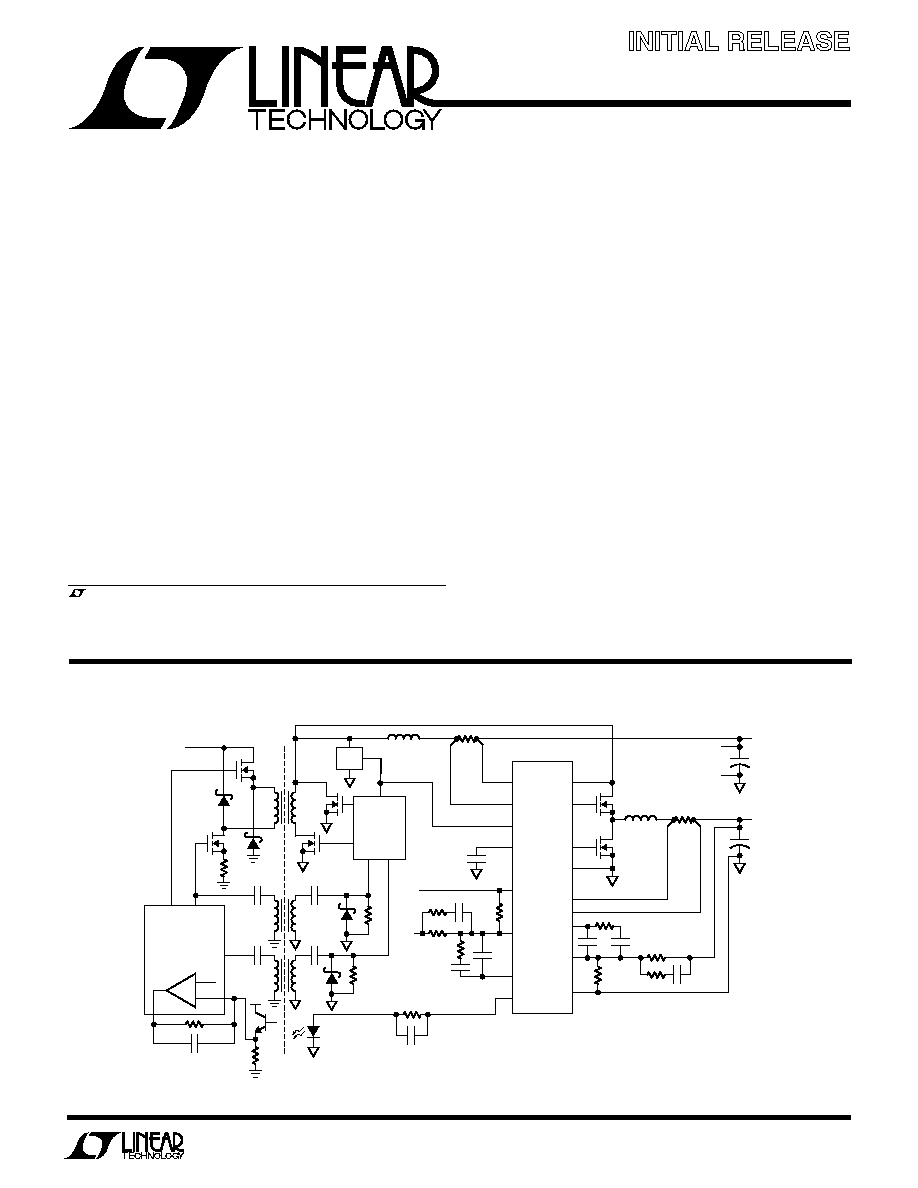
TYPICAL APPLICATIO
U
The LT
®
3804 is a high efficiency step-down switching
regulator with optocoupler feedback control for regulating
multiple outputs in single-secondary winding isolated
power supplies.
The LT3804 contains an error amplifier and an optocoupler
driver to regulate the first (main) output. For the second
output regulation, the LT3804 contains a complete PWM
controller to drive dual synchronous N-channel MOSFETs.
With leading edge modulation, it operates with either
current or voltage mode control of the primary side. The
LT3804 is synchronized to the falling edge of the trans-
former secondary winding and can be used in single-
ended or double-ended isolated power converter topolo-
gies. A user selectable discontinuous conduction mode
improves light load efficiency.
True differential Kelvin sensing is used for each output
feedback amplifier to achieve high regulation accuracy
and design simplicity. Other features include soft start,
current limit and power good flags.
, LTC and LT are registered trademarks of Linear Technology Corporation.
s
48V Input Isolated DC/DC Converters
s
Multiple Output Power Supplies
s
Offline Converters
s
DC/DC Power Modules
Secondary Side Dual
Output Controller with Opto Driver
June 2003
IN2
IN1
OUT2
OUT1
V
CC
BIAS
V
OUT1
3.3V
AT 15A
BG
SG
LT3781
ISOLATION
BOUNDARY
C
OUT1
, C
OUT2
: SANYO POSCAP 4TPE680MF 680
µ
F/4V
L1, L2: SUMIDA CEP125-IR8MC-H
Q1-Q4: SILICONIX Si7892DP
V
IN
36V
TO 72V
V
REF
V
C
V
FB
TG
·
·
Q1
Q2
L2
1.8
µ
H
0.003
·
·
+
V
OUT2
1.8V
AT 15A
·
·
C
OUT1
+
LTC1693-1
CL1N
CL1P
V
CC
CSET
GNDS1
V
FB1
V
AOUT1
OPTO
SYNC
TGATE
SW
BGATE
PGND
CL2N
V
FB2
Q4
x2
x2
Q3
CL2P
V
AOUT2
GNDS2
C
OUT2
+
L1
1.8
µ
H
V
OS1
+
V
OS1
V
OS1
+
V
OS1
1.5k
3.01k
604
LT3804
2.74k
390pF
3804 F01
0.003
Figure 1. 250kHz, 3.3V and 1.8V Output Isolated DC/DC Converter (Simplified Schematic)
LT3804
2
3804i
V
CC
Supply Voltage .................................................. 26V
BOOST Pin Voltage with Respect to SW Pin ............ 10V
BOOST Pin Voltage with Respect to GND Pin .......... 35V
SYNC Pin Voltage (Note 2) ..................................... 30V
GNDS1 Pin Voltage ................................................... 1V
GNDS2 Pin Voltage ................................................... 1V
Operating Junction Temperature Range
LT3804E (Note 3) ..............................40
°
C to 125
°
C
Storage Temperature Range ..................65
°
C to 150
°
C
Lead Temperature (Soldering, 10 sec).................. 300
°
C
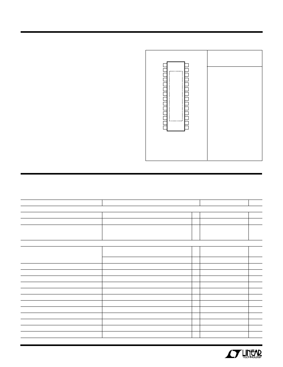
ORDER PART
NUMBER
T
JMAX
= 125
°
C,
JA
= 38
°
C/W
EXPOSED PAD IS SGND (PIN 29)
MUST BE CONNECTED TO PCB
LT3804EFE
ABSOLUTE AXI U
RATI GS
W
W
W
U
PACKAGE/ORDER I FOR ATIO
U
U
W
(Note 1)
ELECTRICAL CHARACTERISTICS
The
q
denotes the specifications which apply over the full operating
temperature range, otherwise specifications are at T
A
= 25
°
C. V
CC
= 11V, GNDS1=GNDS2=0V, operating maximum V
CC
= 25V, no load
on any outputs, unless otherwise noted.
Consult LTC Marketing for parts specified with wider operating temperature ranges.
FE PACKAGE
28-LEAD PLASTIC TSSOP
1
2
3
4
5
6
7
TOP VIEW
28
27
26
25
24
23
22
8
9
10
11
12
13
14
21
20
19
18
17
16
15
CL1P
CL1N
I
LCOMP2
BOOST
TGATE
SW
CSET
SYNC
SS2
PGIN1
PGIN2
GNDS2
GNDS1
V
FB2
I
LCOMP1
GBIAS
BGATE
V
CC
PGND
OPTO
V
AOUT1
CL2N
CL2P
PGOOD
V
FB1
SS1
BGS
V
AOUT2
29
PARAMETER
CONDITIONS
MIN
TYP
MAX
UNITS
Overall
Supply Voltage (V
CC
)
q
8
25
V
Supply Current (I
VCC
)
V
AOUT2
1.2V (Switching Off)
9
13
mA
BOOST Pin Current
V
BOOST
= V
SW
+ 8V, 0V
V
SW
24V
TGATE High
2
3
mA
TGATE Low
2
3
mA
Voltage Amplifier V
A1
,V
A2
Reference Voltage (V
REF1
,V
REF2
)
Common Mode:
±
20mV (0
°
C to 125
°
C)
0.591
0.6
0.609
V
(40
°
C to 125
°
C)
q
0.587
0.609
V
V
REF
over Common Mode:
±
100mV
3
3
mV
V
FB1
, V
FB2
Pin Input Current
V
FB1
= V
REF1
, V
FB2
= V
REF2
0.2
0.5
µ
A
Remote Ground Pin (GNDS1,GNDS2) Current
100mV
GNDS1, GNDS2
100mV
q
50
100
µ
A
V
AOUT1
High at OA1 Threshold 1.5V
V
FB1
= V
REF1
10mV, I
VAOUT1
= 50
µ
A
1.75
V
V
AOUT1
High at OA1 Threshold 1.25V
V
FB1
= V
REF1
10mV, I
VAOUT1
= 50
µ
A
1.45
V
V
AOUT1
Low
V
FB1
= V
REF1
+ 10mV, I
VAOUT1
= 100
µ
A
0.7
V
V
AOUT2
High
V
FB2
= V
REF2
10mV, I
VAOUT2
= 50
µ
A
4.5
V
V
AOUT2
Low
V
FB2
= V
REF2
+ 10mV, I
VAOUT2
= 100
µ
A
0.8
V
V
AOUT1
Source Current
q
100
230
400
µ
A
V
AOUT2
Source Current
q
70
150
250
µ
A
Open-Loop Gain
100
dB
Gain Bandwidth Product
10
MHz
Soft-Start Current (SS1,SS2)
5
10
24
µ
A
LT3804
3
3804i
ELECTRICAL CHARACTERISTICS
The
q
denotes the specifications which apply over the full operating
temperature range, otherwise specifications are at T
A
= 25
°
C. V
CC
= 11V, GNDS1=GNDS2=0V, operating maximum V
CC
= 25V, no load
on any outputs, unless otherwise noted.
Note 1: Absolute Maximum Ratings are those values beyond which the life
of a device may be impaired.
Note 2: If highter than 30V on SYNC pin is needed, add a 10k
resistor in
series with the pin.
Note 3: The LT3804E is guaranteed to meet performance specifications
from 0
°
C to 70
°
C. Specifications over the 40
°
C to 85
°
C operating
temperature range are assured by design, characterization and correlation
with statistical process controls.
PARAMETER
CONDITIONS
MIN
TYP
MAX
UNITS
Opto Driver Amplifier OA1
OA1 Upper Threshold
q
1.4
1.55
1.65
V
OA1 Threshold Hysteresis
0.25
V
OA1 Voltage Gain (V
OPTO
/V
AOUT1
)
1.2V < V
OPTO
< 4V, R
OPTO
= 1k
q
5.6
6
6.4
V
V
OPTO
High
V
AOUT1
= 0.9V, I
OPTO
= 10mA
q
4.5
5.2
6
V
V
OPTO
Low
V
FB1
= V
REF1
10mV, R
OPTO
= 1k
q
0
0.1
0.25
V
I
OPTO
Short-Circuit Current Limit
V
FB1
=V
REF1
10mV, GNDS1 = 0V,
V
OPTO
= 4V
q
50
25
12
mA
Power Good
Power Good Window Threshold
(PGIN1-GNDS1, PGIN2-GNDS2)
100mV < GNDS1, GNDS2 < 100mV
0.85
1.15
V
REF
Input Current (PGIN1,PGIN2)
0V < PGIN1, PGIN2 < 1V
0.2
0.35
µ
A
Delay Time for Power Bad
25mV Overdrive on PGIN1,PGIN2
q
100
200
300
µ
s
Output Low (PGOOD)
2mA into the Pin
q
150
300
mV
Current Limit Amplifier CA1, CA2
Current Limit Threshold (CL1P-CL1N, CL2P-CL2N)
Common Mode Voltage from 0V to V
CC
2.5V
V
AOUT1
= 1.2V, V
AOUT2
= 2.5V,
q
40
50
60
mV
BGATE Off Threshold at (V
CL2P
-V
CL2N
), BGS Pin Float
Commond Mode Voltage from 0V to V
CC
2.5V
0
8
15
mV
Switching Off Threshold at I
LCOMP2
V
ILCOMP2
0.15
V
Input Current (CL1P, CL1N, CL2P, CL2N)
V
CL2P
= V
CL1N
, V
CL2P
= V
CL2N
100
µ
A
Oscillator
Switching Frequency
C
S
= 500pF (NO SYNC)
q
170
200
240
kHz
C
S
= 333pF (NO SYNC)
q
240
280
340
kHz
C
S
= 200pF (NO SYNC)
q
400
470
570
kHz
Synchronization Frequency Range
C
S
= 500pF
q
245
400
kHz
C
S
= 333pF
q
345
500
kHz
C
S
= 200pF
q
575
800
kHz
CSET Ramp Valley Voltage
C
S
= 1000pF (NO SYNC)
0.90
1.15
1.4
V
CSET Peak-to-Peak Voltage
C
S
= 1000pF (NO SYNC)
2.4
V
Synchronization Pulse Threshold on SYNC Pin
Falling Edge V
SYNC
2.5
V
Maximum Duty Cycle
V
FB2
= V
REF2
5mV, C
S
> 333pF
q
75
80
%
Gate Drivers (TGATE, BGATE)
V
GBIAS
I
GBIAS
< 25mA
q
7.5
8
8.5
V
V
TGATE
High (V
TGATE
V
SW
)
I
TGATE
< 50mA, V
BOOST
= V
GBIAS
0.5V
5
6
7.5
V
V
BGATE
High
I
BGATE
< 50mA
q
5
6
7.5
V
V
TGATE
Low (V
TGATE
-V
SW
)
I
TGATE
< 50mA
q
0.5
V
V
BGATE
Low
I
BGATE
< 50mA
q
0.5
V
Peak Gate Drive Current
10nF Load
1
A
Gate Drive Rise and Fall Time
1nF Load
25
ns
LT3804
4
3804i
V
GBIAS
vs I
GBIAS
Over Junction
Temperature
I
CC
vs V
CC
(Switching Off)
Voltage Amplifier V
A1
, V
A2
Gain
and Phase
V
REF
vs V
CC
,
FREQ vs V
CC
CSET vs Switching Frequency
V
REF
vs Temperature
Switching Frequency vs
Temperature
G
BIAS
vs I
GBIAS
(Charging 2.2
µ
F)
Current Limit Amplifier CA1 Gain
at V
CC
= 11V, V
CL2N
= 5V
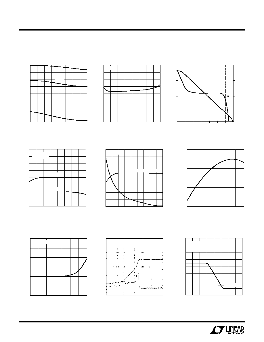
TYPICAL PERFOR A CE CHARACTERISTICS
U
W
I
GBIAS
(mA)
0
V
GBIAS
(V)
8.1
8.0
7.9
7.8
7.7
3804 G01
10
20
26
40
°
C
25
°
C
125
°
C
V
CC
(V)
8
10
12
14
16
18
20
22
24
I
CC
(mA)
13
12
11
10
9
8
7
6
5
3804 G02
T
A
= 25
°
C
FREQUENCY (Hz)
10
GAIN (dB)
120
80
40
0
20
PHASE (DEG)
0
50
100
150
180
3804 G03
PHASE
0dB, 10MHz
(111
°
)
GAIN
100
1k
10k
100k
1M
10M 100M
T
A
= 25
°
C
V
CC
(V)
10
15
20
25
V
REF
(mV)
3
2
1
0
1
FREQ (kHz)
1
0
1
3804 G04
V
REF
CSET = 500pF
T
A
= 25
°
C
FREQ
TIME
0
I
GBIAS
(mA)
300
250
200
150
100
50
0
V
GBIAS
(V)
12
10
8
6
4
2
0
500
µ
s
3804 G08
1ms
V
GBIAS
C
GBIAS
= 2.2
µ
F
T
A
= 25
°
C
I
GBIAS
V
CL2P
V
CL2N
(mV)
40
30
50
60
70
V
AOUT2
(V)
8
7
6
5
4
3
2
1
0
3804 G09
CSET PEAK
V
CC
= 11V
V
CL2N
= 5V
T
A
= 25
°
C
CSET VALLEY
CSET (pF)
FREQUENCY (kHz)
400 500 600 700 800 900 1000
3804 G05
100 200 300
800
600
400
200
1.00
0.95
0.90
0.85
0.80
0.75
0.70
CSET
MAXIMUM DUTY CYCLE
MAXIMUM DUTY CYCLE
T
A
= 25
°
C
JUNCTION TEMPERATURE (
°
C)
40
V
REF
(V)
0.602
0.601
0.600
0.599
0.598
0.587
0.596
25
75
3804 G06
20
0
50
100
125
JUNCTION TEMPERATURE (
°
C)
40
SWITCHING FREQUENCY (kHz)
215
210
205
200
195
25
75
3804 G07
20
0
50
100
125
CSET = 500pF

LT3804
5
3804i
CL1P (Pin 1): Current Limit Amplifier CA1 Positive Input.
CA1 drives optocoupler when the first output is in current
limit.The threshold is set at 50mV.
CL1N (Pin 2): Current Limit Amplifier CA1 Negative Input.
When used, CL1N is connected to the output, and CL1P is
connected to the other end of the output current sense
resistor.
I
LCOMP2
(Pin 3): Current Limit Amplifier CA2 Compensa-
tion Node. At second output current limit, CA2 pulls down
on this pin to regulate output current.
BOOST (Pin 4): Topside (Boosted) Driver Supply.This pin
is used to bootstrap and supply the topside power switch
gate drive circuitry. In normal operation V
BOOST
is powered
from the internally generated 8V GBIAS; V
BOOST
= V
SW
+ 8V
when TGATE is on.
TGATE (Pin 5): Topside (Boosted) N-Channel MOSFET
Driver. When TGATE is on, the voltage is equal to V
SW
+ 6V.
SW (Pin 6): Switch Node Connection to Inductor.
CSET (Pin 7): Oscillator Frequency Setting Pin.The capaci-
tor from this pin to ground sets the PWM switching
frequency.
SYNC (Pin 8): Synchronization Input. This pin should be
connected to the secondary side output of the power
transformer with a series resistor. A filtering capacitor of
10pf is recommended.
SS2 (Pin 9): Soft-Start for the Second Output. A capacitor
on this pin sets the output ramp-up rate. The typical time
for SS2 to reach the programmed level is: (C · 0.6V)/10
µ
A.
PGIN1 (Pin 10): First Output Power Good Input.The volt-
age setting resistor divider should be connected to GNDS1
if remote sensing is used.
PGIN2 (Pin 11): Second Output Power Good Input. The
voltage setting resistor divider should be connected to
GNDS2 if remote sensing is used.
GNDS2 (Pin 12): Second Output Remote Ground Sensing.
GNDS1 (Pin 13): First Output Remote Ground Sensing.
V
FB2
(Pin 14): Voltage Amplifier V
A2
Inverting Input. A
resistor divider to this pin sets the second output voltage.
The reference voltage at this pin is V
REF2
(0.6V referred to
remote sensing ground GNDS2).
V
AOUT2
(Pin 15): Voltage Amplifier V
A2
Output.
BGS (Pin 16): Bottom Gate Switching Control. CA2 moni-
tors the inductor current and prohibits BGATE from turn-
ing on when the inductor current is low (below 8mV across
the current sense resistor R
S2
) allowing discontinous
mode operation and avoiding reverse inductor current.
Grounding BGS disables this function, so that the PWM is
always in continuous mode except during start-up.
SS1 (Pin 17): Soft-Start for the First Output. A capacitor on
this pin sets the output ramp-up rate. The typical time for
SS1 to reach the programmed level is: (C · 0.6V)/10
µ
A.
V
FB1
(Pin 18): Voltage Amplifier V
A1
Inverting Input. A
resistor divider to this pin sets the first output voltage. The
reference voltage at this pin is V
REF1
(0.6V referred to
remote sensing ground GNDS1).
PGOOD (Pin 19): Power Good. PGOOD goes high to
indicate power good only when both PGIN1 and PGIN2
sense power good. A pull up resistor is required on this pin
if the power good function is used.
CL2P (Pin 20): Second 0utput Current Limit Amplifier
CA2 Positive Input.The threshold is set at 50mV.
CL2N (Pin 21): Current Limit Amplifier CA2 Negative
Input. When used, CL2N is connected to the output
capacitor, and CL2P is connected to the other end of the
output current sense resistor.
V
AOUT1
(Pin 22): Voltage Amplifier VA1 Output.
OPTO (Pin 23): Optocoupler Driver. A resistor to the opto
diode is required to set the optocoupler bias current.
Maximum sourcing current is 10mA at 5V.
PGND (Pin 24): Ground of the Bottom Side N-Channel
MOSFET Driver.
V
CC
(Pin 25): Supply of the Chip. A low ESR capacitor is
required to bypass the supply.
BGATE (Pin 26): Bottom Side N-Channel MOSFET Driver.
GBIAS (Pin 27): 8V Regulator Output for Boostrapping
V
BOOST
. A bypass capacitor of at least 2
µ
F is needed.
I
LCOMP1
(Pin 28): Current Limit Amplifier CA1 Compensa-
tion Node . When the first output is in current limit, CA1
pulls down V
AOUT1
pin to regulate the first output current.
Exposed Pad (Pin 29): Signal Ground. Must be electrically
connected on PCB.
U
U
U
PI FU CTIO S