 | –≠–ª–µ–∫—Ç—Ä–æ–Ω–Ω—ã–π –∫–æ–º–ø–æ–Ω–µ–Ω—Ç: LT5506 | –°–∫–∞—á–∞—Ç—å:  PDF PDF  ZIP ZIP |
LT5517
1
5517f
BPF
5V
V
CC
BPF
RF
+
RF
≠
LPF
LT5517
I
OUT
+
I
OUT
≠
0
∞
2xLO
EN
ENABLE
2xLO
INPUT
LPF
DSP
Q
OUT
+
Q
OUT
≠
90
∞
˜
2
5517 F01
LNA
VGA
VGA
s
Wireless Infrastructure
s
High Linearity Direct Conversion I/Q Receiver
s
High Linearity I/Q Demodulator
, LTC and LT are registered trademarks of Linear Technology Corporation.
s
RF Input Frequency Range: 40MHz to 900MHz
s
High IIP3: 21dBm at 800MHz
s
High IIP2: 58dBm at 800MHz
s
I/Q Gain Mismatch: 0.3dB Max
s
I/Q Phase Mismatch: 0.7
∞
s
Noise Figure: 12.4dB at 800MHz
s
Conversion Gain: 3.3dB at 800MHz
s
Baseband Bandwidth: 130MHz
s
Single Ended, 50
Matched 2XLO Input
s
Shutdown Mode
s
16-Lead QFN (4mm
◊
4mm) Package
with Exposed Pad
40MHz to 900MHz
Quadrature Demodulator
Figure 1. High Signal-Level I/Q Demodulator for 450MHz Infrastructure Receiver
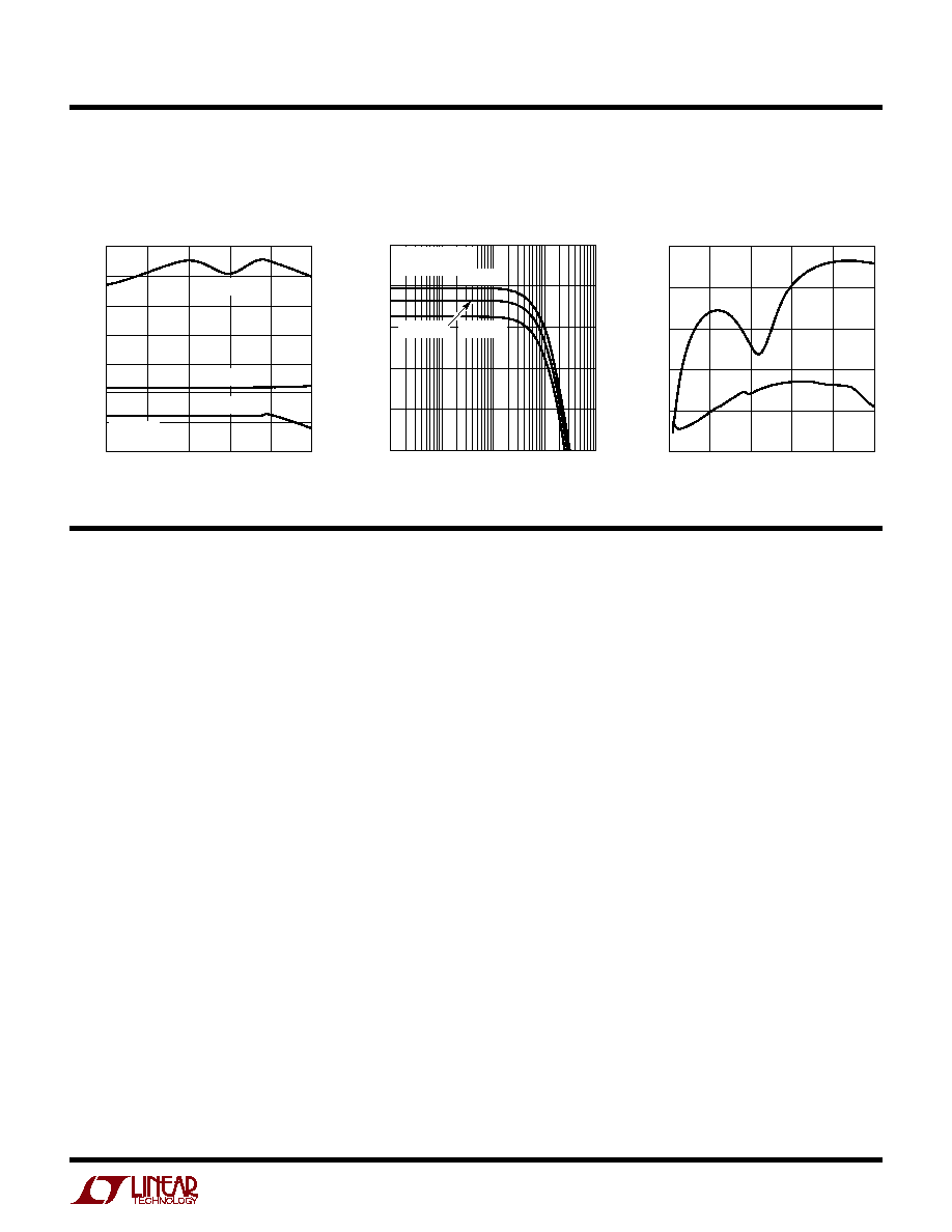
I/Q Output Power, IM3, IM2
vs RF Input Power
The LT
Æ
5517 is a 40MHz to 900MHz quadrature demodu-
lator optimized for high linearity receiver applications
where high dynamic range is important. It is suitable for
communications receivers where an RF or IF signal is
directly converted into I and Q baseband signals with a
bandwidth up to 130MHz. The LT5517 incorporates bal-
anced I and Q mixers, LO buffer amplifiers and a precision,
broadband quadrature generator derived from an on-chip
divide-by-two circuit.
The superior linearity and low noise performance of the
LT5517 is achieved across its full frequency range. A well-
balanced divide-by-two circuit generates precision quadra-
ture LO carriers to drive the I mixer and the Q mixer.
Consequently, the outputs of the I-channel and the
Q-channel are well matched in amplitude, and their phases
are 90
∞
apart. The LT5517 also provides excellent 50
impedance matching at the 2XLO port across its entire
frequency range.
RF INPUT POWER (dBm)
≠18
≠100
P
OUT
, IM3, IM2 (dBm/TONE)
≠80
≠60
≠40
≠20
0
20
P
OUT
IM3
IM2
≠14
≠10
≠6
≠2
5517 F01b
2
T
A
= 25
∞
C
P
2XLO
= ≠10dBm
f
2XLO
= 1602MHz
f
RF1
= 799.9MHz
f
RF2
= 800.1MHz
FEATURES
DESCRIPTIO
U
APPLICATIO S
U
TYPICAL APPLICATIO
U
LT5517
2
5517f
Power Supply Voltage ............................................ 5.5V
Enable Voltage .................................................... 0V, V
CC
2XLO Voltage (10dBm Equivalent) ..........................
±
1V
RF
+
to RF
≠
Differential Voltage
(10dBm Equivalent) .................................................
±
2V
Operating Ambient Temperature ..............≠40
∞
C to 85
∞
C
Storage Temperature Range ................. ≠ 65
∞
C to 125
∞
C
Maximum Junction Temperature .......................... 125
∞
C
ORDER PART
NUMBER
Consult LTC Marketing for parts specified with wider operating temperature ranges.
LT5517EUF
ABSOLUTE AXI U
RATI GS
W
W
W
U
PACKAGE/ORDER I FOR ATIO
U
U
W
(Note 1)
T
A
= 25
∞
C. V
CC
= 5V, EN = V
CC
, f
RF1
= 799.9MHz, f
RF2
= 800.1MHz,
f
2XLO
= 1602MHz, P
2XLO
= ≠10dBm, unless otherwise noted. (Notes 2, 3) (Test circuit shown in Figure 2)
PARAMETER
CONDITIONS
MIN
TYP
MAX
UNITS
RF Frequency Range
40 to 900
MHz
2XLO Frequency Range
80 to 1800
MHz
2XLO Power
≠15 to 0
dBm
2XLO Port Return Loss
Internally Matched to a 50
Source
20
dB
Conversion Gain
Voltage Gain, Load Impedance = 1k
0
3.3
dB
Gain Variation vs Temperature
≠40
∞
C to 85
∞
C
0.01
dB/
∞
C
Noise Figure
12.4
dB
Input 3rd Order Intercept
2-Tone, ≠10dBm/Tone,
f = 200kHz
21
dBm
Input 2nd Order Intercept
2-Tone, ≠10dBm/Tone,
f = 200kHz
58
dBm
Input 1dB Compression
10
dBm
Baseband Bandwidth
130
MHz
I/Q Gain Mismatch
(Note 4)
≠0.3
0.03
0.3
dB
I/Q Phase Mismatch
(Note 4)
≠3.5
0.7
3.5
deg
Output Impedance
Differential
120
2XLO to RF Leakage
≠69
dBm
LO to RF Leakage
≠80
dBm
RF to 2XLO Isolation
63
dB
AC ELECTRICAL CHARACTERISTICS
T
JMAX
= 125
∞
C,
JA
= 37
∞
C/W
UF PART
MARKING
5517
16 15 14 13
5
6
7
8
TOP VIEW
UF PACKAGE
16-LEAD (4mm
◊
4mm) PLASTIC QFN
EXPOSED PAD (PIN 17) IS GND,
MUST BE SOLDERED TO PCB
9
10
11
12
4
3
2
1
GNDRF
RF
+
RF
≠
GNDRF
V
CC
GND
2XLO
GND
I
OUT
+
I
OUT
≠
Q
OUT
+
Q
OUT
≠
EN
V
CC
V
CC
V
CC
17
LT5517
3
5517f
DC ELECTRICAL CHARACTERISTICS
T
A
= 25
∞
C. V
CC
= 5V unless otherwise noted.
PARAMETER
CONDITIONS
MIN
TYP
MAX
UNITS
Supply Voltage
4.5
5.25
V
Supply Current
70
90
110
mA
Shutdown Current
EN = LOW
0.1
20
µ
A
Turn-On Time
(Note 5)
200
ns
Turn-Off Time
(Note 5)
300
ns
EN = HIGH (On)
1.6
V
EN = LOW (Off)
1.3
V
EN Input Current
V
ENABLE
= 5V
2
µ
A
Output DC Offset Voltage
f
LO
= 1602MHz, P
LO
= ≠10dBm
0.5
30
mV
(
I
OUT
+
≠ I
OUT
≠
,
Q
OUT
+
≠ Q
OUT
≠
)
Output DC Offset Variation vs Temperature
≠ 40
∞
C to 85
∞
C
7
µ
V/
∞
C
Note 1: Absolute Maximum Ratings are those values beyond which the life
of a device may be impaired.
Note 2: Tests are performed as shown in the configuration of Figure 2.
Note 3: Specifications over the ≠ 40
∞
C to 85
∞
C temperature range are
assured by design, characterization and correlation with statistical process
control.
Note 4: Measured at P
2XLO
= ≠10dBm and output frequency = 1MHz.
Note 5: Turn ON and Turn OFF times are based on rise and fall times of the
output baseband voltage with RF input power of ≠10dBm.
TYPICAL PERFOR A CE CHARACTERISTICS
U
W
Supply Current vs Supply Voltage
Conv Gain, NF, IIP3
vs RF Input Frequency
SUPPLY VOLTAGE (V)
4.5
SUPPLY CURRENT (mA)
80
90
5.5
5517 G01
70
60
4.75
5
5.25
110
100
T
A
= 85
∞
C
T
A
= 25
∞
C
T
A
= ≠40
∞
C
RF INPUT FREQUENCY (MHz)
0
0
GAIN (dB), NF (dB), IIP3 (dBm)
5
15
20
25
200
400 500
900
5517 G02
10
100
300
600 700 800
IIP3
NF
CONV GAIN
P
2XLO
= ≠10dBm
V
CC
= 5V
T
A
= 25
∞
C
RF INPUT FREQUENCY (MHz)
0
30
IIP2 (dBm)
40
60
70
80
200
400 500
900
5517 G03
50
100
300
600 700 800
P
2XLO
= ≠10dBm
V
CC
= 5V
T
A
= 25
∞
C
IIP2 vs RF Input Frequency
f
RF
= 800MHz, P
2XLO
= ≠10dBm, unless otherwise noted. (Test circuit shown in Figure 2)
LT5517
4
5517f
I/Q Output Power, IM3
vs RF Input Power
RF INPUT POWER (dBm)
≠18
≠100
P
OUT
, IM3 (dBm/TONE)
≠80
≠60
≠40
≠20
0
20
≠14
≠10
≠6
≠2
5517 G04
2
T
A
= 85
∞
C
T
A
= 25
∞
C
T
A
= ≠40
∞
C
f
2XLO
= 1602MHz
V
CC
= 5V
f
RF1
= 799.9MHz
f
RF2
= 800.1MHz
OUTPUT POWER
IM3
RF INPUT FREQUENCY (MHz)
0
GAIN MISMATCH (dB)
0
0.20
0.40
800
5517 G05
≠0.20
≠0.40
≠0.80
200
400
600
100
300
500
700
900
≠0.60
0.80
0.60
T
A
= 85
∞
C
T
A
= 25
∞
C
T
A
= ≠40
∞
C
P
2XLO
= ≠10dBm
f
BB
= 1MHz
V
CC
= 5V
RF INPUT FREQUENCY (MHz)
0
≠6
PHASE MISMATCH (DEGREE)
≠4
0
2
4
200
400 500
900
5517 G06
≠2
100
300
600 700 800
6
T
A
= 85
∞
C
T
A
= 25
∞
C
T
A
= ≠40
∞
C
P
2XLO
= ≠10dBm
f
BB
= 1MHz
V
CC
= 5V
I/Q Gain Mismatch
vs RF Input Frequency
I/Q Phase Mismatch
vs RF Input Frequency
Conv Gain, IIP3 vs Supply Voltage
NF vs 2XLO Input Power
Conv Gain, IIP3
vs 2XLO Input Power
SUPPLY VOLTAGE (V)
4.5
16
20
28
5.25
5517 G07
12
8
4.75
5
5.5
4
0
24
IIP3
CONV GAIN (dB), IIP3 (dBm)
T
A
= 85
∞
C
T
A
= 25
∞
C
T
A
= ≠40
∞
C
f
2XLO
= 1602MHz
V
CC
= 5V
CONV GAIN
f
RF1
= 799.9MHz
f
RF2
= 800.1MHz
2XLO INPUT POWER (dBm)
≠15
NF (dB)
10
12
14
≠3
5517 G08
8
6
4
≠12
≠9
≠6
0
f
RF
= 800MHz
f
RF
= 400MHz
f
RF
= 200MHz
f
RF
= 40MHz
T
A
= 25
∞
C
V
CC
= 5V
2XLO INPUT POWER (dBm)
≠15
0
CONV GAIN (dB), IIP3 (dBm)
4
8
12
16
20
24
IIP3
≠12
≠9
≠6
≠3
5517 G09
0
T
A
= 85
∞
C
T
A
= 25
∞
C
T
A
= ≠40
∞
C
f
2XLO
= 1602MHz
V
CC
= 5V
f
RF1
= 799.9MHz
f
RF2
= 800.1MHz
CONV GAIN
IIP2 vs 2XLO Input Power
LO-RF Leakage
vs 2XLO Input Power
2XLO INPUT POWER (dBm)
≠15
IIP2 (dBm)
45
50
55
≠6
0
5517 G10
40
35
30
≠12
≠9
≠3
60
65
70
T
A
= 85
∞
C
T
A
= 25
∞
C
T
A
= ≠40
∞
C
f
2XLO
= 1602MHz
V
CC
= 5V
2XLO INPUT POWER (dBm)
≠15
≠120
LO-RF LEAKAGE (dBm)
≠110
≠100
≠90
≠80
≠70
≠60
≠12
≠9
≠6
≠3
5517 G11
0
T
A
= 25
∞
C
V
CC
= 5V
f
2XLO
= 1600MHz
f
2XLO
= 800MHz
f
2XLO
= 80MHz
2XLO-RF Leakage
vs 2XLO Input Power
2XLO INPUT POWER (dBm)
≠15
≠120
2XLO-RF LEAKAGE (dBm)
≠110
≠100
≠90
≠80
≠70
≠60
≠12
≠9
≠6
≠3
5517 G12
0
T
A
= 25
∞
C
V
CC
= 5V
f
2XLO
= 1600MHz
f
2XLO
= 800MHz
f
2XLO
= 80MHz
TYPICAL PERFOR A CE CHARACTERISTICS
U
W
f
RF
= 800MHz, P
2XLO
= ≠10dBm, unless otherwise noted. (Test circuit shown in Figure 2)
LT5517
5
5517f
U
U
U
PI FU CTIO S
GNDRF (Pins 1, 4): Ground Pins for RF Termination.
These pins are not internally connected, and should be
connected to the PCB ground plane for best RF isolation.
RF
+
, RF
≠
(Pins 2, 3): Differential RF Input Pins. These pins
are internally biased to 2.30V. These two pins should be
DC blocked when connected to ground or other matching
components. The inputs can be terminated in a single-
ended configuration, but differential input drive is pre-
ferred for best performance. An external matching network
is required for impedance transformation.
EN (Pin 5): Enable Pin. When the input voltage is higher
than 1.6V, the circuit is completely turned on. When the
input voltage is less than 1.3V, the circuit is turned off.
V
CC
(Pins 6, 7, 8, 12): Power Supply Pins. These pins
should be decoupled using 1000pF and 0.1
µ
F capacitors.
GND (Pins 9, 11): Ground Pins. These pins are internally
tied together and to the Exposed Pad. They should be
connected to the PCB ground plane.
2XLO (Pin 10): 2XLO Input Pin. This pin is internally
biased to 1V. The input signal's frequency should be twice
that of the desired demodulator LO frequency. The pin
should be AC coupled with an external DC blocking
capacitor.
Q
OUT
≠
, Q
OUT
+
(Pins 13, 14): Differential Baseband Output
Pins of the Q-Channel. The internal DC bias voltage is
V
CC
≠ 0.78V for each pin.
I
OUT
≠
, I
OUT
+
(Pins 15, 16): Differential Baseband Output
Pins of the I-Channel. The internal DC bias voltage is
V
CC
≠ 0.78V for each pin.
Exposed Pad (Pin 17): Ground Return for the Entire IC.
This pin must be soldered to the printed circuit board
ground plane.
RF-LO Isolation
vs RF Input Power
Conv Gain
vs Baseband Frequency
RF, 2XLO Port Return Loss
vs Frequency
RF INPUT POWER (dBm)
≠15
100
110
120
5
5517 G13
90
80
≠10
≠5
0
10
70
60
50
RF-LO ISOLATION (dB)
f
RF
= 800MHz
f
RF
= 400MHz
f
RF
= 40MHz
T
A
= 25
∞
C
V
CC
= 5V
BASEBAND FREQUENCY (MHz)
≠2
CONV GAIN (dB)
0
2
4
6
0.1
10
100
1000
5517 G14
≠4
1
T
A
= 85
∞
C
f
2XLO
= 1602MHz
V
CC
= 5V
T
A
= ≠40
∞
C
T
A
= 25
∞
C
FREQUENCY (GHz)
0
RETURN LOSS (dB)
≠10
≠5
0
1.60
5517 G15
≠15
RF
LO
≠20
≠25
0.40
0.80
1.20
2
TYPICAL PERFOR A CE CHARACTERISTICS
U
W
f
RF
= 800MHz, P
2XLO
= ≠10dBm, unless otherwise noted. (Test circuit shown in Figure 2)
LT5517
6
5517f
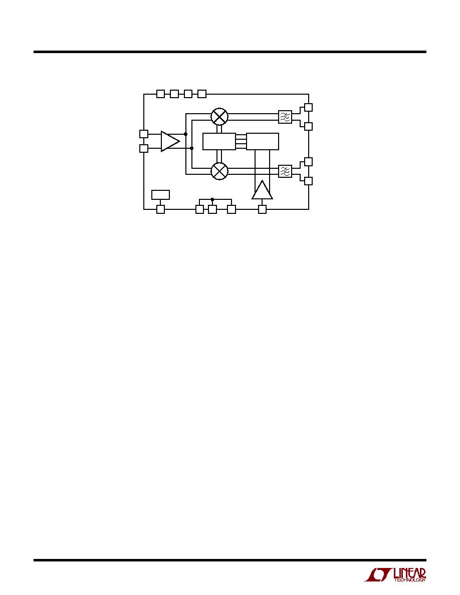
BLOCK DIAGRA
W
RF
+
I
OUT
+
2XLO
˜
2
0
∞
BIAS
16
I
OUT
≠
15
Q
OUT
+
14
Q
OUT
≠
13
LO BUFFERS
LPF
I-MIXER
LPF
Q-MIXER
2
6
V
CC
5
EN
9
GND GND EXPOSED
PAD
7
V
CC
8
V
CC
12
V
CC
RF
≠
5517 BD
3
11
17
10
RF AMP
90
∞
LT5517
7
5517f
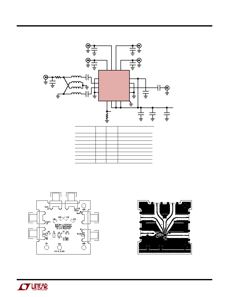
Figure 2. Evaluation Circuit Schematic
Figure 4. Component Side Layout of Evaluation Board
Figure 3. Component Side Silkscreen of Evaluation Board
TEST CIRCUIT
I
OUT
≠
J3
I
OUT
+
J4
RF
J1
Q
OUT
+
J5
Q
OUT
≠
J6
C10
3.3pF
R2
0
C11
1nF
C12
1nF
J2
2XLO
C5
1nF
EN
5
6
7
8
16 15 14 13
17
R1
100k
C3
0.1
µ
F
C4
2.2
µ
F
V
CC
LT5517
GNDRF
RF
+
RF
≠
GNDRF
V
CC
GND
2XLO
GND
1
2
3
4
12
11
10
9
I
OUT
+
I
OUT
≠
Q
OUT
+
Q
OUT
≠
EN
V
CC
V
CC
V
CC
REFERENCE
DESIGNATION
VALUE
SIZE
PART NUMBER
C1,C2,C5,C11,C12
1nF
0603
AVX 06033A102JAT1A
C3
0.1
µ
F
0603
TAIYO YUDEN EMK107B
C4
2.2
µ
F
0603
TAIYO YUDEN JMK107B
C10
3.3pF
0603
AVX 06033A3R3KAT2A
C13 TO C16
10pF
0805
AVX 08055A100ZAT1A
R1
100k
0603 OPTIONAL
R2
0
0603
JUMPER, OPTIONAL
T1
1:4
M/A COM MABAES0054
5517 F02
C15
10pF
C16
10pF
C1
1nF
T1
MABAES0054
C2
1nF
C13
10pF
C14
10pF
LT5517
8
5517f
APPLICATIO S I FOR ATIO
W
U
U
U
The LT5517 is a direct I/Q demodulator targeting high
linearity receiver applications. It consists of an RF ampli-
fier, I/Q mixers, a quadrature LO carrier generator and bias
circuitry.
The RF signal is applied to the inputs of the RF amplifier,
and is then demodulated into I-channel and Q-channel
baseband signals using precision quadrature LO signals,
which are internally generated using a divide-by-two cir-
cuit. The demodulated I/Q signals are lowpass filtered
internally with a ≠3dB bandwidth of 130MHz. The differen-
tial outputs of the I-channel and Q-channel are well matched
in amplitude and their phases are 90
∞
apart across the full
frequency range from 40MHz to 900MHz.
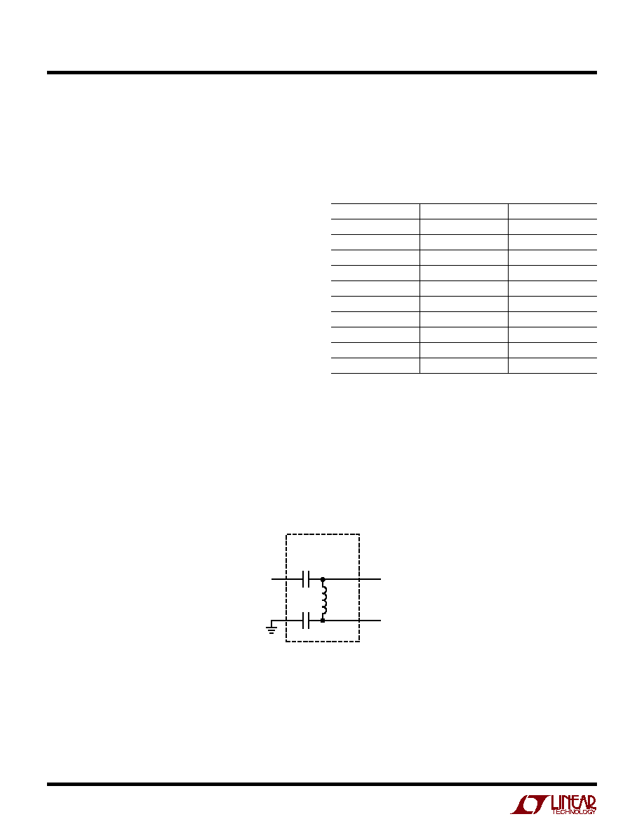
RF Input Port
Differential drive is recommended for the RF inputs as
shown in Figure 2. A low loss 1:4 transformer is used on
the demonstration board for a wide bandwidth input
impedance match and to assure good noise figure and
maximum demodulator gain. Single-ended to differential
conversion can also be implemented using narrowband
L-C circuits to produce the required balanced waveforms
at the RF
+
and RF
≠
inputs using three discrete elements as
shown in Figure 5. Nominal values are listed in Table 1. (In
practice, these values should be compensated according
to the parasitics of the PCB.) The conversion gain and NF
of the receiver are similar to those of the transformer-
coupled demo board, because the single-ended to differ-
ential conversion has a 1:4 impedance transformation,
similar to the transformer.
Table 1. The Component Values of Matching Network L
SH
, C
S1
and C
S2
FREQUENCY (MHz)
L
SH
(nH)
C
S1
, C
S2
(pF)
40
437
71.1
100
169
28.6
200
80.8
14.3
300
51.5
9.6
400
37
7.2
500
28.3
5.8
600
22.6
4.9
700
18.5
4.2
800
15.6
3.7
900
13.5
3.3
The differential impedance of the RF inputs is listed in
Table 2. The RF inputs may also be terminated in a single-
ended configuration. In this case either the RF
+
or the RF
≠
input can be simply AC coupled to a 50
source, while the
other RF input is connected to ground with a 1nF capacitor.
Note, however, that this will result in degraded conversion
gain and noise figure in most cases.
Figure 5. RF Input Matching Network at 800MHz
L
SH
15.6nH
TO RF
+
TO RF
≠
MATCHING NETWORK
C
S1
3.7pF
RF
INPUT
5517 F05
C
S2
3.7pF
LT5517
9
5517f
Table 2. RF Input Differential Impedance
FREQUENCY
DIFFERENTIAL INPUT
DIFFERENTIAL S11
(MHz)
IMPEDANCE (
)
MAG
ANGLE(
∞
)
40
240.1-j10.3
0.665
≠0.8
100
245.5-j25.9
0.664
≠2.5
200
236.8-j50.0
0.664
≠5.1
300
223.6-j70.5
0.663
≠7.6
400
207.9-j86.3
0.662
≠10.2
500
190.6-j98.1
0.660
≠12.7
600
173.2-j105.8
0.657
≠15.3
700
156.2-j110.2
0.655
≠17.9
800
141.2-j111.8
0.651
≠20.4
900
129.5-j114.5
0.650
≠22.9
2XLO Input Port
To ease the interface of the receiver with the external 2XLO
input, the 2XLO port is designed with on-chip 50
imped-
ance matching up to 2GHz. The input is internally biased
at 1V. A 1nF DC blocking capacitor is required when
connected to the external 2XLO source.
The 2XLO frequency is required to be twice the desired
operating frequency in order for the chip to generate the
APPLICATIO S I FOR ATIO
W
U
U
U
quadrature Local Oscillator (LO) signals for the demodu-
lator. The on-chip divide-by-two circuit delivers well-
matched, quadrature LO carriers to the I mixer and the Q
mixer.
I-Channel and Q-Channel Outputs
Each of the I-channel and Q-channel outputs is internally
connected to V
CC
though a 60
resistor. The output DC
bias voltage is V
CC
≠ 0.78V. The outputs can be DC coupled
or AC coupled to the external loads. The differential output
impedance of the demodulator is 120
in parallel with a
10pF internal capacitor, forming a lowpass filter with a
≠3dB corner frequency at 130MHz. The load impedance,
R
LOAD
, should be larger than 600
to assure full gain. The
gain is reduced by 20 ∑ log(1 + 120
/R
LOAD
) in dB when
the differential output is terminated by R
LOAD
. For ex-
ample, the gain is reduced by 6.85dB when each output pin
is connected to a 50
load (or 100
differential loads).
The output should be taken differentially (or by using
differential-to-single-ended conversion) for best RF per-
formance, including NF and IM2. Proper filtering of the
unwanted high frequency mixing product is also impor-
tant to maintain the highest linearity. A convenient
Figure 6. RF Input Equivalent Circuit with External Broadband Matching
3
2
V
CC
LT5517
RF
+
1
2
3
5
4
RF
≠
5517 F06
250
2.30V
RF
J1
C10
3.3pF
C1
1nF
T1
MABAES0054
C2
1nF
LT5517
10
5517f
Figure 7. I/Q Output Equivalent Circuit
APPLICATIO S I FOR ATIO
W
U
U
U
15
16
V
CC
10pF
I
OUT
+
I
OUT
≠
5517 F07
13
14
10pF
Q
OUT
+
Q
OUT
≠
60
60
60
60
approach is to terminate each output with a shunt capaci-
tor. The capacitor value can be optimized depending upon
the operating frequency and the specific PCB layout.
The phase relationship between the I-channel output sig-
nal and the Q-channel output signal is fixed. When the LO
input frequency is higher than the RF input frequency, then
the Q-channel outputs (Q
OUT
+
, Q
OUT
≠
) lead the I-channel
outputs (I
OUT
+
, I
OUT
≠
) by 90
∞
.
When the LO input frequency is lower than the RF input
frequency, then the Q-channel outputs lag the I-channel
outputs by 90
∞
. Note that the phase relationship of the I-
and Q-channel outputs relative to the LO can vary by 180
∞
,
depending on start-up conditions. This is the nature of a
frequency divider-based quadrature phase generator.
When AC output coupling is used, the resulting highpass
filter's ≠3dB roll-off frequency is defined by the R-C
constant of the blocking capacitor and R
LOAD
, assuming
R
LOAD
> 600
.
Care should be taken when the demodulator's outputs are
DC coupled to the external load to make sure that the I/Q
mixers are biased properly. If the current drain from the
outputs exceeds 6mA, there can be significant degrada-
tion of the linearity performance. Each output can sink no
more than 13mA when connected to an external load with
a DC voltage higher than V
CC
≠ 0.78V.
LT5517
11
5517f
UF Package
16-Lead Plastic QFN (4mm
◊
4mm)
(Reference LTC DWG # 05-08-1692)
U
PACKAGE DESCRIPTIO
4.00
±
0.10
(4 SIDES)
NOTE:
1. DRAWING CONFORMS TO JEDEC PACKAGE OUTLINE MO-220 VARIATION (WGGC)
2. ALL DIMENSIONS ARE IN MILLIMETERS
3. DIMENSIONS OF EXPOSED PAD ON BOTTOM OF PACKAGE DO NOT INCLUDE
MOLD FLASH. MOLD FLASH, IF PRESENT, SHALL NOT EXCEED 0.15mm ON ANY SIDE
4. EXPOSED PAD SHALL BE SOLDER PLATED
PIN 1
TOP MARK
0.55
±
0.20
16
15
1
2
BOTTOM VIEW--EXPOSED PAD
2.15
±
0.10
(4-SIDES)
0.75
±
0.05
R = 0.115
TYP
0.30
±
0.05
0.65 BSC
0.200 REF
0.00 ≠ 0.05
(UF) QFN 0503
RECOMMENDED SOLDER PAD PITCH AND DIMENSIONS
0.72
±
0.05
0.30
±
0.05
0.65 BSC
2.15
±
0.05
(4 SIDES)
2.90
±
0.05
4.35
±
0.05
PACKAGE OUTLINE
Information furnished by Linear Technology Corporation is believed to be accurate and reliable.
However, no responsibility is assumed for its use. Linear Technology Corporation makes no represen-
tation that the interconnection of its circuits as described herein will not infringe on existing patent rights.

LT5517
12
5517f
Linear Technology Corporation
1630 McCarthy Blvd., Milpitas, CA 95035-7417
(408) 432-1900
q
FAX: (408) 434-0507
q
www.linear.com
©
LINEAR TECHNOLOGY CORPORATION 2004
LT/TP 0104 1K ∑ PRINTED IN USA
RELATED PARTS
PART NUMBER
DESCRIPTION
COMMENTS
Infrastructure
LT5511
High Linearity Upconverting Mixer
RF Output to 3GHz, 17dBm IIP3, Integrated LO Buffer
LT5512
DC-3GHz High Signal Level Downconverting Mixer
DC to 3GHz, 21dBm IIP3, Integrated LO Buffer
LT5515
1.5GHz to 2.5GHz Direct Conversion Quadrature Demodulator
20dBm IIP3, Integrated LO Quadrature Generator
LT5516
0.8GHz to 1.5GHz Direct Conversion Quadrature Demodulator
21.5dBm IIP3, Integrated LO Quadrature Generator
LT5520
1.3GHz to 2.3GHz High Linearity Upconverting Mixer
15.9dBm IIP3, Single Ended, 50
Matched RF and LO Ports
LT5522
600MHz to 2.7GHz High Signal Level Downconverting Mixer
4.5V to 5.25V Supply, 25dBm IIP3 at 900MHz, NF = 12.5dB,
50
Single-Ended RF and LO Ports
RF Power Detectors
LT5504
800MHz to 2.7GHz RF Measuring Receiver
80dB Dynamic Range, Temperature Compensated,
2.7V to 5.25V Supply
LTC
Æ
5505
RF Power Detectors with >40dB Dynamic Range
300MHz to 3GHz, Temperature Compensated, 2.7V to 6V Supply
LTC5507
100kHz to 1000MHz RF Power Detector
100kHz to 1GHz, Temperature Compensated, 2.7V to 6V Supply
LTC5508
300MHz to 7GHz RF Power Detector
44dB Dynamic Range, Temperature Compensated, SC70 Package
LTC5509
300MHz to 3GHz RF Power Detector
36dB Dynamic Range, Low Power Consumption, SC70 Package
LTC5532
300MHz to 7GHz Precision RF Power Detector
Precision V
OUT
Offset Control, Adjustable Gain and Offset
RF Building Blocks
LT5500
1.8GHz to 2.7GHz Receiver Front End
1.8V to 5.25V Supply, Dual-Gain LNA, Mixer, LO Buffer
LT5502
400MHz Quadrature IF Demodulator with RSSI
1.8V to 5.25V Supply, 70MHz to 400MHz IF, 84dB Limiting Gain,
90dB RSSI Range
LT5503
1.2GHz to 2.7GHz Direct IQ Modulator and
1.8V to 5.25V Supply, Four-Step RF Power Control,
Upconverting Mixer
120MHz Modulation Bandwidth
LT5506
500MHz Quadrature IF Demodulator with VGA
1.8V to 5.25V Supply, 40MHz to 500MHz IF, ≠4dB to 57dB
Linear Power Gain, 8.8MHz Baseband Bandwidth
LT5546
500MHz Ouadrature IF Demodulator with
17MHz Baseband Bandwidth, 40MHz to 500MHz IF, 1.8V to 5.25V
VGA and 17MHz Baseband Bandwidth
Supply, ≠7dB to 56dB Linear Power Gain
RF Power Controllers
LTC1757A
RF Power Controller
Multiband GSM/DCS/GPRS Mobile Phones
LTC1758
RF Power Controller
Multiband GSM/DCS/GPRS Mobile Phones
LTC1957
RF Power Controller
Multiband GSM/DCS/GPRS Mobile Phones
LTC4400
SOT-23 RF PA Controller
Multiband GSM/DCS/GPRS Phones, 45dB Dynamic Range,
450kHz Loop BW
LTC4401
SOT-23 RF PA Controller
Multiband GSM/DCS/GPRS Phones, 45dB Dynamic Range,
250kHz Loop BW
LTC4403
RF Power Controller for EDGE/TDMA
Multiband GSM/GPRS/EDGE Mobile Phones