6001_02.pm65
LT6001/LT6002
1
60012f
APPLICATIO S
U
TYPICAL APPLICATIO
U
FEATURES
DESCRIPTIO
U
Gas Sensing
Portable Instrumentation
Battery- or Solar-Powered Systems
Low Voltage Signal Processing
Micropower Active Filters
Ideal for Battery-Powered Applications
� Low Voltage: 1.8V Operation
� Low Current: 16
�
A/Amplifier Max
� Small Packages: DFN, MSOP, SSOP
� Shutdown to 1.5
�A Max (LT6001DD)
Low Offset Voltage: 500
�V Max
Rail-to-Rail Input and Output
Fully Specified on 1.8V and 5V Supplies
Operating Temperature Range: �40
�C to 85�C
Available in 10-Lead and 16-Lead DFN, 8-Lead MSOP
and 16-Lead SSOP Packages
Dual and Quad,
1.8V, 13
�A Precision
Rail-to-Rail Op Amps
, LTC and LT are registered trademarks of Linear Technology Corporation.
All other trademarks are the property of their respective owners.
The LT
�
6001/LT6002 are dual and quad precision rail-to-
rail input and output operational amplifiers. Designed to
maximize battery life in always-on applications, the de-
vices will operate on supplies down to 1.8V while drawing
only 13
�A quiescient current. The low supply current and
low voltage operation is combined with precision specifi-
cations; input offset is guaranteed less than 500
�V. The
performance on 1.8V supplies is fully specified and guar-
anteed over temperature. A shutdown feature in the 10-
lead dual version can be used to extend battery life by
allowing the amplifiers to be switched off during periods
of inactivity.
The LT6001 is available in the 8-Pin MSOP package; a
10-lead version with the shutdown feature is available in a
tiny, dual fine pitch leadless package (DFN). The quad
LT6002 is available in the 16-pin SSOP package and the
16-pin DFN package. These devices are specified over the
commercial and industrial temperature range.
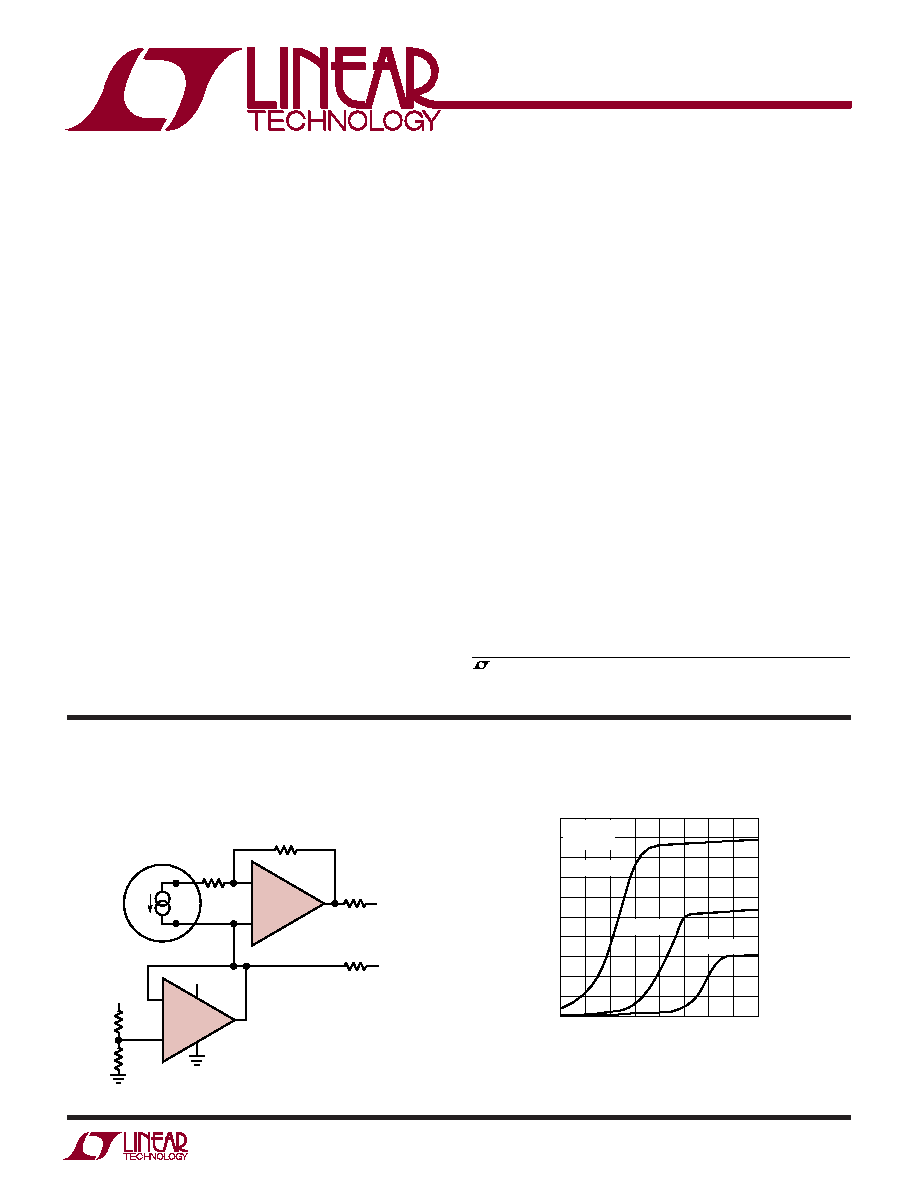
�
+
�V
E
100
330
V
OUT
= 1V IN AIR,
0V WITHOUT OXYGEN
330
+
�
10k
OXYGEN SENSOR
CITY TECHNOLOGY
40X(2)
www.citytech.com
+V
E
1/2 LT6001
200k
V
S
= 1.8V
I
SUPPLY
= 145
�A IN AIR,
45
�A WITHOUT OXYGEN
V
S
V
S
20k
60012 TA01a
�
+
1/2 LT6001
Micropower Oxygen Sensor
Start-Up Characteristics
Supply Current vs Supply Voltage
TOTAL SUPPLY VOLTAGE (V)
0.4
0
SUPPLY CURRENT PER AMPLIFIER (
�
A)
10
25
0.8
1.2
1.4
60012 TA01b
5
20
15
0.6
1.0
1.6
1.8
2.0
A
V
= 1
V
CM
= 0.5V
T
A
= 125
�C
T
A
= 25
�C
T
A
= �55
�C
LT6001/LT6002
60012f
2
DD PART MARKING*
MS8 PART MARKING*
ABSOLUTE AXI U
RATI GS
W
W
W
U
(Note 1)
Total Supply Voltage (V
+
to V
�
) .............................. 18V
Input Current .....................................................
�10mA
SHDN Pin Voltage (Note 7) ............................... V
�
to V
+
Output Short Current Duration (Note 2) ......... Indefinite
Operating Temperature Range (Note 3) ... �40
�C to 85�C
Specified Temperature Range (Note 4) .... �40
�C to 85�C
Junction Temperature ........................................... 150
�C
Junction Temperature (DFN Packages) ................ 125
�C
Storage Temperature Range .................. �65
�C to 150�C
Storage Temperature Range
DFN Packages ................................... �65
�C to 125�C
Lead Temperature (Soldering, 10 sec)
MSOP, SSOP Packages .................................... 300
�C
*Temperature grades are identified on the shipping container. Consult LTC Marketing for parts specified with wider operating temperature ranges.
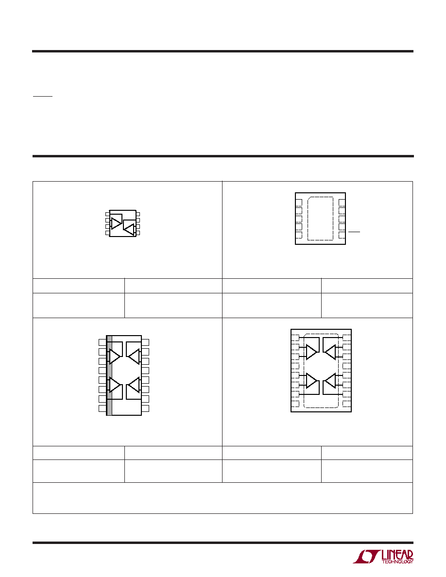
PACKAGE/ORDER I FOR ATIO
U
U
W
ORDER PART NUMBER
LT6001CMS8
LT6001IMS8
ORDER PART NUMBER
LT6001CDD
LT6001IDD
TOP VIEW
DD PACKAGE
10-LEAD (3mm
� 3mm) PLASTIC DFN
10
9
6
7
8
4
5
3
2
1
V
+
OUT B
IN
�
B
IN
+
B
SHDN
OUT A
IN
�
A
IN
+
A
V�
NC
T
JMAX
= 125
�C,
JA
= 160
�C/W (NOTE 2)
UNDERSIDE METAL CONNECTED TO V
�
ORDER PART NUMBER
LT6002CGN
LT6002IGN
ORDER PART NUMBER
DHC PART MARKING*
LT6002CDHC
LT6002IDHC
GN PART MARKING
6002
6002I
T
JMAX
= 150
�C,
JA
= 250
�C/W
1
2
3
4
OUT A
IN
�
A
IN
+
A
V
�
8
7
6
5
V
+
OUT B
IN
�
B
IN
+
B
TOP VIEW
MS8 PACKAGE
8-LEAD PLASTIC MSOP
�
+
�
+
T
JMAX
= 125
�C,
JA
= 160
�C/W (NOTE 2)
UNDERSIDE METAL CONNECTED TO V
�
16
15
14
13
12
11
10
9
1
2
3
4
5
6
7
8
TOP VIEW
DHC PACKAGE
16-LEAD (5mm
� 3mm) DFN
OUT A
IN
�
A
IN
+
A
V
+
IN
+
B
IN
�
B
OUT B
NC
OUT D
IN
�
D
IN
+
D
V
�
IN
+
C
IN
�
C
OUT C
NC
A
D
B
C
1
2
3
4
5
6
7
8
TOP VIEW
GN PACKAGE
16-LEAD NARROW PLASTIC SSOP
16
15
14
13
12
11
10
9
OUT A
IN
�
A
IN
+
A
V
+
IN
+
B
IN
�
B
OUT B
NC
OUT D
IN
�
D
IN
+
D
V
�
IN
+
C
IN
�
C
OUT C
NC
+
�
+
�
�
+
�
+
A
D
B
C
T
JMAX
= 150
�C,
JA
= 135
�C/W
Order Options Tape and Reel: Add #TR
Lead Free: Add #PBF Lead Free Tape and Reel: Add #TRPBF
Lead Free Part Marking:
http://www.linear.com/leadfree/
LTBVD
LTBVD
LBVH
LBVH
6002
6002
LT6001/LT6002
3
60012f
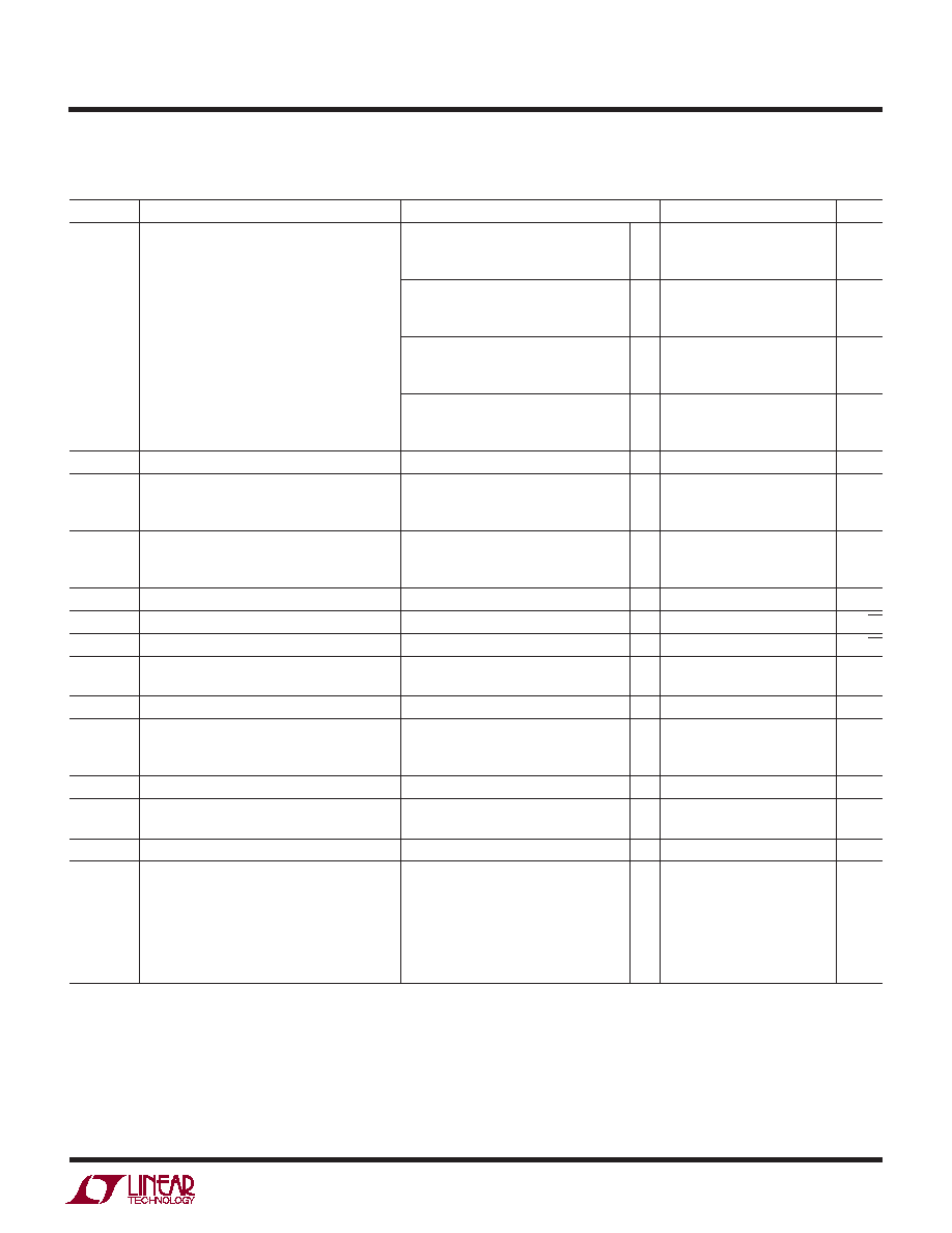
ELECTRICAL CHARACTERISTICS
The
denotes specifications which apply over the full specified temperature
range, otherwise specifications are T
A
= 25
�C. V
S
= 1.8V, 0V, V
CM
= V
OUT
= 0.5V, for the LT6001DD, V
SHDN
= V
+
, unless otherwise
noted.
SYMBOL
PARAMETER
CONDITIONS
MIN
TYP
MAX
UNITS
V
OS
Input Offset Voltage
LT6001MS8, LT6002GN
200
500
�V
0
�C T
A
70�C
700
�V
�40
�C T
A
85�C
850
�V
LT6001DD, LT6002DHC
250
650
�V
0
�C T
A
70�C
850
�V
�40
�C T
A
85�C
1000
�V
V
CM
= V
�
to V
+
LT6001MS8, LT6002GN
400
1000
�V
1300
�V
V
CM
= V
�
to V
+
LT6001DD, LT6002DHC
500
1200
�V
1500
�V
V
OS
/
T
Input Offset Voltage Drift (Note 5)
V
CM
= 0.5V
2
5
�V/�C
I
B
Input Bias Current
V
CM
= 0.5V
�5
�2
nA
V
CM
= V
�
�5
�2
nA
V
CM
= V
+
4
10
nA
I
OS
Input Offset Current
V
CM
= 0.5V
0.2
1
nA
V
CM
= V
�
0.2
1
nA
V
CM
= V
+
0.4
2
nA
Input Noise Voltage
0.1Hz to 10Hz
1.2
�V
P-P
e
n
Input Voltage Noise Density
f = 1kHz
75
nV/
Hz
i
n
Input Current Noise Density
f = 1kHz
25
fA/
Hz
R
IN
Input Resistance
Common Mode (V
CM
= 0V to 0.6V)
3.5
G
Differential
10
25
M
C
IN
Input Capacitance
5
pF
CMRR
Common Mode Rejection Ratio
V
CM
= 0V to 0.6V, 0
�C T
A
70�C
82
96
dB
V
CM
= 0.1V to 0.6V, �40
�C T
A
85�C
82
96
dB
V
CM
= 0V to 1.8V
62
78
dB
Input Voltage Range
0
1.8
V
PSRR
Power Supply Rejection Ratio
V
S
= 1.8V to 6V
80
90
dB
V
CM
= V
O
= 0.5V
Minimum Supply
V
CM
= V
O
= 0.5V
1.8
V
LT6001/LT6002
60012f
4
ELECTRICAL CHARACTERISTICS
The
denotes specifications which apply over the full specified temperature
range, otherwise specifications are T
A
= 25
�C. V
S
= 1.8V, 0V, V
CM
= V
OUT
= 0.5V, for the LT6001DD, V
SHDN
= V
+
, unless otherwise
noted.
SYMBOL
PARAMETER
CONDITIONS
MIN
TYP
MAX
UNITS
A
VOL
Large-Signal Gain
V
O
= 0.25V to 1.25V
R
L
= 100k to GND
25
65
V/mV
R
L
= 100k to GND
20
V/mV
R
L
= 10k to GND
40
125
V/mV
R
L
= 10k to GND
25
V/mV
V
OL
Output Swing Low (Note 6)
Input Overdrive = 30mV
No Load
30
60
mV
I
SINK
= 100
�A
120
200
mV
V
OH
Output Swing High (Note 6)
Input Overdrive = 30mV
No Load
30
60
mV
I
SOURCE
= 100
�A
140
225
mV
R
L
= 10k to GND
160
250
mV
I
SC
Short-Circuit Current
Short to GND
2
4
mA
0
�C T
A
70�C
1
mA
�40
�C T
A
85�C
0.4
mA
Short to V
+
0.7
2
mA
0
�C T
A
70�C
0.4
mA
�40
�C T
A
85�C
0.15
mA
I
S
Supply Current per Amplifier
13
16
�A
0
�C T
A
70�C
22
�A
�40
�C T
A
85�C
24
�A
Total Supply Current in Shutdown (Note 7)
V
SHDN
= 0.3V
0.8
1.5
�A
I
SHDN
SHDN Pin Current (Note 7)
V
SHDN
= 1.8V
0
20
nA
V
SHDN
= 0V
�300
�200
nA
Shutdown Output Leakage Current (Note 7)
V
SHDN
= 0.3V (V
�
V
OUT
V
+
)
20
nA
V
L
SHDN Pin Input Low Voltage (Note 7)
0.3
V
V
H
SHDN Pin Input High Voltage (Note 7)
1.5V
V
t
ON
Turn On Time (Note 7)
V
SHDN
= 0V to 1.8V,
400
�s
R
L
= 10k
t
OFF
Turn Off Time (Note 7)
V
SHDN
= 1.8V to 0V,
100
�s
R
L
= 10k
GBW
Gain Bandwidth Product (Note 8)
Freq = 1kHz
32
50
kHz
0
�C T
A
70�C
28
kHz
�40
�C T
A
85�C
24
kHz
SR
Slew Rate
A
V
= �1, V
OUT
= 0.25V to 1.5V
9
15
V/ms
Measure 0.5V to 1.25V, 0
�C T
A
70�C
7
V/ms
�40
�C T
A
85�C
5
V/ms
FPBW
Full Power Bandwidth (Note 9)
V
OUT
= 1.25V
P-P
2.3
3.8
kHz
LT6001/LT6002
5
60012f
ELECTRICAL CHARACTERISTICS
The
denotes specifications which apply over the full specified temperature
range, otherwise specifications are T
A
= 25
�C. V
S
= 5V, 0V, V
CM
= V
OUT
= 1/2 Supply, for the LT6001DD, V
SHDN
= V
+
, unless otherwise
noted.
SYMBOL
PARAMETER
CONDITIONS
MIN
TYP
MAX
UNITS
V
OS
Input Offset Voltage
LT6001MS8, LT6002GN
200
500
�V
0
�C T
A
70�C
700
�V
�40
�C T
A
85�C
850
�V
LT6001DD, LT6002DHC
250
650
�V
0
�C T
A
70�C
850
�V
�40
�C T
A
85�C
1000
�V
V
CM
= V
�
to V
+
LT6001MS8, LT6002GN
400
1000
�V
1300
�V
V
CM
= V
�
to V
+
LT6001DD, LT6002DHC
500
1200
�V
1500
�V
V
OS
/
T
Input Offset Voltage Drift (Note 5)
V
CM
= V
S
/2
2
5
�V/�C
I
B
Input Bias Current
V
CM
= V
S
/2
�6
�2
nA
V
CM
= V
�
�6
�2
nA
V
CM
= V
+
4
12
nA
I
OS
Input Offset Current
V
CM
= V
S
/2
0.2
1.2
nA
V
CM
= V
�
0.2
1.2
nA
V
CM
= V
+
0.4
2.4
nA
Input Noise Voltage
0.1Hz to 10Hz
1.2
�V
P-P
e
n
Input Voltage Noise Density
f = 1kHz
75
nV/
Hz
i
n
Input Current Noise Density
f = 1kHz
25
fA/
Hz
R
IN
Input Resistance
Common Mode (V
CM
= 0V to 3.8V)
3.5
G
Differential
8.5
25
M
C
IN
Input Capacitance
5
pF
CMRR
Common Mode Rejection Ratio
V
CM
= 0V to 3.8V, 0
�C T
A
70�C
90
105
dB
V
CM
= 0.1V to 3.8V, �40
�C T
A
85�C
90
105
dB
V
CM
= 0V to 5V
70
86
dB
Input Voltage Range
0
5
V
PSRR
Power Supply Rejection Ratio
V
S
= 1.8V to 6V
80
90
dB
V
CM
= V
O
= 0.5V
Minimum Supply
1.8
V
A
VOL
Large-Signal Gain
V
O
= 0.5V to 4.5V
R
L
= 100k to V
S
/2
30
60
V/mV
R
L
= 100k to V
S
/2
25
V/mV
R
L
= 10k to V
S
/2
16
25
V/mV
R
L
= 10k to V
S
/2
10
V/mV
R
L
= 10k to GND
160
1000
V/mV
R
L
= 10k to GND
80
V/mV