Äîêóìåíòàöèÿ è îïèñàíèÿ www.docs.chipfind.ru
1
LTC1142/LTC1142L/LTC1142HV
S
FEATURE
D
U
ESCRIPTIO
The LTC
®
1142/LTC1142L/LTC1142HV are dual synchro-
nous step-down switching regulator controllers featuring
automatic Burst Mode
TM
operation to maintain high efficien-
cies at low output currents. The devices are composed of two
separate regulator blocks, each driving a pair of external
complementary power MOSFETs, at switching frequencies
up to 250kHz, using a constant off-time current mode archi-
tecture providing constant ripple current in the inductor.
The operating current level for both regulators is user pro-
grammable via an external current sense resistor. Wide input
supply range allows operation from 3.5V* to 18V (20V
maximum). Constant off-time architecture provides low drop-
out regulation limited only by the R
DS(ON)
of the external
MOSFET and resistance of the inductor and current sense
resistor.
The LTC1142 series is ideal for applications requiring dual
output voltages with high conversion efficiencies over a wide
load current range in a small amount of board space.
Dual High Efficiency
Synchronous Step-Down
Switching Regulators
s
Dual Outputs: 3.3V and 5V or User Programmable
s
Ultra-High Efficiency: Over 95% Possible
s
Current Mode Operation for Excellent Line and Load
Transient Response
s
High Efficiency Maintained over 3 Decades of
Output Current
s
Low Standby Current at Light Loads: 160
µ
A/Output
s
Independent Micropower Shutdown: I
Q
< 40
µ
A
s
Wide V
IN
Range: 3.5V to 20V
s
Very Low Dropout Operation: 100% Duty Cycle
s
Synchronous FET Switching for High Efficiency
s
Available in Standard 28-Pin SSOP
s
Notebook and Palmtop Computers
s
Battery-Operated Digital Devices
s
Portable Instruments
s
DC Power Distribution Systems
U
S
A
O
PPLICATI
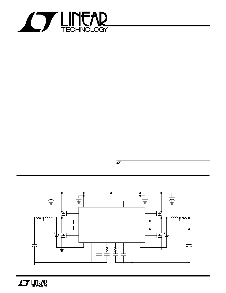
Figure 1. High Efficiency Dual 3.3V, 5V
U
A
O
PPLICATI
TYPICAL
1000pF
+
+
+
1000pF
PDRIVE 3
SENSE
+
3
SENSE
3
NDRIVE 3
PGND3 SGND3 C
T3
I
TH3
I
TH5
C
T5
SGND5 PGND5
NDRIVE 5
SENSE
5
SENSE
+
5
PDRIVE 5
V
IN3
SHUTDOWN 3
SHUTDOWN 5
V
IN5
LTC1142HV
C
T5
390pF
4
3
25
27
13
11
17
18
R
C5
1k
C
C3
3300pF
C
C5
3300pF
C
T3
560pF
R
C3
1k
0.22
µ
F
2
24
16
10
9
15
14
20
23
1
28
6
V
OUT5
5V/2A
C
OUT5
220
µ
F
10V
×
2
R
SENSE5
0.05
P-CH
Si9430DY
L2
50
µ
H
D2
1N5818
N-CH
Si9410DY
0V = NORMAL
>1.5V = SHUTDOWN
0.22
µ
F
C
IN5
22
µ
F
25V
×
2
C
IN3
22
µ
F
25V
×
2
P-CH
Si9430DY
N-CH
Si9410DY
D1
1N5818
C
OUT3
220
µ
F
10V
×
2
L1
50
µ
H
R
SENSE3
0.05
V
OUT3
3.3V/2A
V
IN
5.2V TO 18V
R
SENSE3,
R
SENSE5
: SL-C1-1/2-1R050J
L1, L2: COILTRONICS CTX50-2-MP
PINS 5, 7, 8, 19, 21, 22: NC
1142 F01
NOTE: COMPONENTS OPTIMIZED FOR HIGHEST EFFICIENCY, NOT MINIMUM BOARD SPACE.
+
, LTC and LT are registered trademarks of Linear Technology Corporation.
Burst Mode
is a trademark of Linear Technology Corporation.
*For LTC1142L-ADJ only.

2
LTC1142/LTC1142L/LTC1142HV
A
U
G
W
A
W
U
W
A
R
BSOLUTE
XI
TI
S
Input Supply Voltage (Pins 10, 24)
LTC1142, LTC1142L-ADJ ..................... 16V to 0.3V
LTC1142HV, LTC1142HV-ADJ ............. 20V to 0.3V
Continuous Output Current (Pins 6, 9, 20, 23) .... 50mA
Sense Voltages (Pins 1, 14, 15, 28).......... 13V to 0.3V
Operating Ambient Temperature Range ...... 0
°
C to 70
°
C
Extended Commercial
Temperature Range ........................... 40
°
C to 85
°
C
Junction Temperature (Note 1) ............................ 125
°
C
Storage Temperature Range ................ 65
°
C to 150
°
C
Lead Temperature (Soldering, 10 sec) ................. 300
°
C
ORDER PART
NUMBER
Consult factory for Industrial and Military grade parts.
ORDER PART
NUMBER
W
U
U
PACKAGE/ORDER I FOR ATIO
LTC1142CG
LTC1142HVCG
LTC1142HVCG-ADJ
LTC1142LCG-ADJ
1
2
3
4
5
6
7
8
9
10
11
12
13
14
SENSE
+
1
V
FB1
SHUTDOWN 1
SGND1
PGND1
NDRIVE 1
NC
NC
PDRIVE 2
V
IN2
C
T2
INT V
CC2
I
TH2
SENSE
2
28
27
26
25
24
23
22
21
20
19
18
17
16
15
G PACKAGE, 28-LEAD SSOP
T
JMAX
= 125
°
C,
JA
= 95
°
C/W
TOP VIEW
LTC1142-ADJ
SENSE
1
I
TH1
INT V
CC1
C
T1
V
IN1
PDRIVE 1
NC
NC
NDRIVE 2
PGND2
SGND2
SHUTDOWN 2
V
FB2
SENSE
+
2
1
2
3
4
5
6
7
8
9
10
11
12
13
14
28
27
26
25
24
23
22
21
20
19
18
17
16
15
G PACKAGE, 28-LEAD SSOP
T
JMAX
= 125
°
C,
JA
= 95
°
C/W
TOP VIEW
LTC1142
SENSE
3
I
TH3
INT V
CC3
C
T3
V
IN3
PDRIVE 3
NC
NC
NDRIVE 5
NC
PGND5
SGND5
SHUTDOWN 5
SENSE
+
5
SENSE
+
3
SHUTDOWN 3
SGND 3
PGND 3
NC
NDRIVE 3
NC
NC
PDRIVE 5
V
IN5
C
T5
INT V
CC5
I
TH5
SENSE
5
ELECTRICAL C
C
HARA TERISTICS
T
A
= 25
°
C, V
10
= V
24
= 10V, V
SHUTDOWN
= 0V, unless otherwise noted.
SYMBOL
PARAMETER
CONDITIONS
MIN
TYP
MAX
UNITS
V
2
, V
16
Feedback Voltage
LTC1142HV-ADJ, LTC1142L-ADJ : V
10
, V
24
= 9V
q
1.21
1.25
1.29
V
I
2
, I
16
Feedback Current
LTC1142HV-ADJ, LTC1142L-ADJ
q
0.2
1
µ
A
V
OUT
Regulated Output Voltage
LTC1142, LTC1142HV
3.3V Output
I
LOAD
= 700mA, V
24
= 9V
q
3.23
3.33
3.43
V
5V Output
I
LOAD
= 700mA, V
10
= 9V
q
4.90
5.05
5.20
V
V
OUT
Output Voltage Line Regulation
V
10,
V
24
= 7V to 12V, I
LOAD
= 50mA
40
0
40
mV
Output Voltage Load Regulation
Figure 1 Circuit
3.3V Output
5mA < I
LOAD
< 2A
q
40
65
mV
5V Output
5mA < I
LOAD
< 2A
q
60
100
mV
Output Ripple (Burst Mode)
I
LOAD
= 0A
50
mV
P-P
I
10
, I
24
Input DC Supply Current (Note 2)
LTC1142
Normal Mode
4V < V
10
, V
24
< 12V
1.6
2.1
mA
Sleep Mode
4V < V
24
< 12V, 6V < V
10
< 12V
160
230
µ
A
Shutdown
V
SD1
= V
SD2
= 2.1V, 4V < V
10
, V
24
< 12V
10
20
µ
A
Input DC Supply Current (Note 2)
LTC1142HV, LTC1142HV-ADJ
Normal Mode
4V < V
10
, V
24
< 18V
1.6
2.3
mA
Sleep Mode
4V < V
24
< 18V, 6V < V
10
< 18V
160
250
µ
A
Shutdown
V
SD1
= V
SD2
= 2.1V, 4V < V
10
, V
24
< 18V
10
22
µ
A

3
LTC1142/LTC1142L/LTC1142HV
ELECTRICAL C
C
HARA TERISTICS
T
A
= 25
°
C, V
10
= V
24
= 10V, V
SHUTDOWN
= 0V, unless otherwise noted.
40
°
C
T
A
85
°
C (Note 4), V
10
= V
24
= 10V, unless otherwise noted.
V
2
, V
16
Feedback Voltage
LTC1142HV-ADJ Only: V
10
, V
24
= 9V
1.21
1.25
1.29
V
I
2
, I
16
Feedback Current
LTC1142HV-ADJ Only
0.2
1
µ
A
V
OUT
Regulated Output Voltage
LTC1142, LTC1142HV
3.3V Output
I
LOAD
= 700mA, V
24
= 9V
3.17
3.33
3.40
V
5V Output
I
LOAD
= 700mA, V
10
= 9V
4.85
5.05
5.20
V
I
10
, I
24
Input DC Supply Current (Note 2)
LTC1142
Normal Mode
4V < V
10
, V
24
< 12V
1.6
2.4
mA
Sleep Mode
4V < V
24
< 12V, 6V < V
10
< 12V
160
260
µ
A
Shutdown
V
SHUTDOWN
= 2.1V, 4V < V
10
, V
24
< 12V
10
22
µ
A
Input DC Supply Current (Note 2)
LTC1142HV-ADJ, LTC1142HV
Normal Mode
4V < V
10
, V
24
< 18V
1.6
2.6
mA
Sleep Mode
4V < V
24
< 18V, 6V < V
10
< 18V
160
280
µ
A
Shutdown
V
SHUTDOWN
= 2.1V, 4V < V
10
, V
24
< 12V
10
24
µ
A
Input DC Supply Current (Note 2)
LTC1142L-ADJ (Note 5)
Normal Mode
3.5V < V
10
, V
24
< 12V
1.6
2.4
mA
Sleep Mode
3.5V < V
10
, V
24
< 12V
160
260
µ
A
Shutdown
V
SD1
= V
SD2
= 2.1V, 3.5V < V
10
, V
24
< 12V
10
22
µ
A
V
1
V
28
Current Sense Threshold Voltage
LTC1142HV-ADJ, LTC1142L-ADJ
V
15
V
14
V
14
= V
28
= V
OUT
+ 100mV, V
2
= V
16
= V
REF
+ 25mV
25
mV
V
14
= V
28
= V
OUT
100mV, V
2
= V
16
= V
REF
25mV
130
150
170
mV
LTC1142, LTC1142HV
V
28
= V
OUT
+ 100mV (Forced)
25
mV
V
28
= V
OUT
100mV (Forced)
125
150
175
mV
LTC1142, LTC1142HV
V
14
= V
OUT
+ 100mV (Forced)
25
mV
V
14
= V
OUT
100mV (Forced)
125
150
175
mV
V
SHUTDOWN
Shutdown Pin Threshold
0.55
0.8
2
V
t
OFF
Off-Time (Note 3)
C
T
= 390pF, I
LOAD
= 700mA
3.8
5
6
µ
s
SYMBOL
PARAMETER
CONDITIONS
MIN
TYP
MAX
UNITS
Input DC Supply Current (Note 2)
LTC1142L-ADJ (Note 5)
Normal Mode
3.5V < V
10
, V
24
< 12V
1.6
2.1
mA
Sleep Mode
3.5V < V
10
, V
24
< 12V
160
230
µ
A
Shutdown
V
SD1
= V
SD2
= 2.1V, 3.5V < V
10
, V
24
< 12V
10
20
µ
A
V
1
V
28
Current Sense Threshold Voltage
LTC1142HV-ADJ, LTC1142L-ADJ
V
15
V
14
V
14
= V
28
= V
OUT
+ 100mV, V
2
= V
16
= V
REF
+ 25mV
25
mV
V
14
= V
28
= V
OUT
100mV, V
2
= V
16
= V
REF
25mV
q
130
150
170
mV
LTC1142, LTC1142HV
V
28
= V
OUT
+ 100mV (Forced)
25
mV
V
28
= V
OUT
100mV (Forced)
q
130
150
170
mV
LTC1142, LTC1142HV
V
14
= V
OUT
+ 100mV (Forced)
25
mV
V
14
= V
OUT
100mV (Forced)
q
130
150
170
mV
V
SHUTDOWN
Shutdown Pin Threshold
0.5
0.8
2
V
I
SHUTDOWN
Shutdown Pin Input Current
0V < V
SHUTDOWN
< 8V, V
10
, V
24
= 16V
1.2
5
µ
A
I
11
, I
24
C
T
Pin Discharge Current
V
OUT
in Regulation, V
SENSE
= V
OUT
50
70
90
µ
A
V
OUT
= 0V
2
10
µ
A
t
OFF
Off-Time (Note 3)
C
T
= 390pF, I
LOAD
= 700mA
4
5
6
µ
s
t
r
, t
f
Driver Output Transition Times
C
L
= 3000pF (Pins 6, 9, 20, 23), V
10
, V
24
= 6V
100
200
ns

4
LTC1142/LTC1142L/LTC1142HV
ELECTRICAL C
C
HARA TERISTICS
The
q
denotes specifications which apply over the full operating
temperature range.
Note 1: T
J
is calculated from the ambient temperature T
A
and power
dissipation P
D
according to the following formula:
LTC1142CG: T
J
= T
A
+ (P
D
×
95
°
C/ W)
Note 2: This current is for one regulator block. Total supply current is the
sum of Pins 10 and 24 currents. Dynamic supply current is higher due to
the gate charge being delivered at the switching frequency. See the
Applications Information section.
Note 3: In applications where R
SENSE
is placed at ground potential, the off-
time increases approximately 40%.
Note 4: The LTC1142/LTC1142HV-ADJ/LTC1142HV/LTC1142L-ADJ are
not tested and quality-assurance sampled at 40
°
C to 85
°
C. These
specifications are guaranteed by design and/or correlation.
Note 5: The LTC1142L-ADJ allows operation down to V
IN
= 3.5V.
C
C
HARA TERISTICS
U
W
A
TYPICAL PERFOR
CE
5V Output Efficiency
LOAD CURRENT (A)
0.01
EFFICIENCY (%)
100
95
90
85
0.1
1
1142 G01
2
V
IN
= 6V
V
IN
= 10V
3.3V Output Efficiency
LOAD CURRENT (A)
0.01
EFFICIENCY (%)
100
95
90
85
0.1
1
1142 G02
2
V
IN
= 5V
V
IN
= 10V
5V Efficiency vs Input Voltage
INPUT VOLTAGE (V)
0
EFFICIENCY (%)
100
98
96
94
92
90
88
86
84
82
80
16
1142 G03
4
8
12
20
FIGURE 1 CIRCUIT
V
OUT
= 5V
I
LOAD
= 1A
I
LOAD
= 100mA
3.3V Efficiency vs Input Voltage
Load Regulation
LOAD CURRENT (A)
0
V
OUT
(mV)
20
0
20
40
60
80
100
2.0
1142 G06
0.5
1.0
1.5
2.5
FIGURE 1 CIRCUIT
R
SENSE
= 0.05
V
IN
= 6V
V
IN
= 6V
V
IN
= 12V
V
OUT
= 5V
V
OUT
= 3.3V
V
IN
= 12V
INPUT VOLTAGE (V)
0
V
OUT
(mV)
40
30
20
10
0
10
20
30
40
16
1142 G05
4
8
12
20
FIGURE 1 CIRCUIT
I
LOAD
= 1A
Line Regulation
INPUT VOLTAGE (V)
0
EFFICIENCY (%)
100
98
96
94
92
90
88
86
84
82
80
16
1142 G04
4
8
12
20
FIGURE 1 CIRCUIT
V
OUT
= 3.3V
I
LOAD
= 1A
I
LOAD
= 100mA

5
LTC1142/LTC1142L/LTC1142HV
C
C
HARA TERISTICS
U
W
A
TYPICAL PERFOR
CE
INPUT VOLTAGE (V)
0
SUPPLY CURRENT (mA)
2.1
1.8
1.5
1.2
0.9
0.6
0.3
0
2
10
14
1142 G07
8
18
4
6
12
16
PER REGULATOR BLOCK
NOT INCLUDING
GATE CHARGE CURRENT
PINS 10, 24
ACTIVE MODE
SLEEP MODE
INPUT VOLTAGE (V)
0
SUPPLY CURRENT (
µ
A)
20
18
16
14
12
10
8
6
4
2
0
2
10
14
1142 G08
8
18
4
6
12
16
PER REGULATOR BLOCK
PINS 10, 24
V
SHUTDOWN
= 2V
V
IN
V
OUT
VOLTAGE (V)
0
NORMALIZED FREQUENCY
12
1142 G09
2
6
8
1.6
1.4
1.2
1.0
0.8
0.6
0.4
0.2
0
4
10
70°C
0°C
25°C
V
OUT
= 5V
OPERATING FREQUENCY (kHz)
20
GATE CHARGE CURRENT (mA)
140
28
24
20
16
12
8
4
0
1142 G10
80
260
200
Q
N
+ Q
P
= 100nC
Q
N
+ Q
P
= 50nC
OUTPUT VOLTAGE (V)
0
OFF-TIME (
µ
s)
80
70
60
50
40
30
20
10
0
4
1142 G11
1
2
3
5
V
SENSE
= V
OUT
V
OUT
= 5V
V
OUT
= 3.3V
PI FU CTIO S
U
U
U
Operating Frequency vs
V
IN
V
OUT
TEMPERATURE (°C)
0
SENSE VOLTAGE (mV)
175
150
125
100
75
50
25
0
80
1142 G12
20
40
60
100
MAXIMUM
THRESHOLD
MINIMUM
THRESHOLD
Current Sense Threshold Voltage
Supply Current in Shutdown
Off-Time vs Output Voltage
DC Supply Current
Gate Charge Supply Current
LTC1142/LTC1142HV
SENSE
+
3 (Pin 1): The (+) Input to the 3.3V Section
Current Comparator. A built-in offset between Pins 1 and
28 in conjunction with R
SENSE3
sets the current trip
threshold for the 3.3V section.
SHUTDOWN 3 (Pin 2): When grounded, the 3.3V section
operates normally. Pulling Pin 2 high holds both MOSFETs
off and puts the 3.3V section in micropower shutdown
mode. Requires CMOS logic-level signal with t
r
, t
f
< 1
µ
s.
Do not "float" Pin 2.
SGND3 (Pin 3): The 3.3V section small-signal ground
must be routed separately from other grounds to the ()
terminal of the 3.3V section output capacitor.
PGND3 (Pin 4): The 3.3V section driver power ground
connects to source of N-channel MOSFET and the ()
terminal of the 3.3V section input capacitor.
NC (Pin 5): No Connection.
NDRIVE 3 (Pin 6): High Current Drive for Bottom N-Channel
MOSFET, 3.3V Section. Voltage swing at Pin 6 is from
ground to V
IN3
.