Äîêóìåíòàöèÿ è îïèñàíèÿ www.docs.chipfind.ru
1
LTC1143/LTC1143L
LTC1143L-ADJ
s
Dual Outputs
LTC1143, LTC1143L: 3.3V, 5V
LTC1143L-ADJ: Dual Adjustable
s
Very High Efficiency: Over 95% Possible
s
Current Mode Operation for Excellent Line and Load
Transient Response
s
High Efficiency Maintained over Three Decades of
Output Current
s
Low Standby Current at Light Loads: 160
µ
A/Output
s
Logic-Controlled Shutdown (LTC1143, LTC1143L)
s
Wide V
IN
Range: 3.5V to 16V
(LTC1143L, LTC1143L-ADJ)
s
Very Low Dropout Operation: 100% Duty Cycle
s
Available in Narrow 16-Pin SO Package
The LTC1143 series is a dual step-down switching regulator
controller featuring automatic Burst Mode
TM
operation to
maintain high efficiencies at low output currents. This
device is composed of two separate regulator blocks,
each driving an external power MOSFET at switching
frequencies up to 400kHz using a constant off-time current
mode architecture. Both fixed and adjustable voltages are
available.
The operating current level for both regulators is user-
programmable via an external current sense resistor.
Wide input supply range allows operation from 4V to 14V
(16V maximum). The LTC1143L and LTC1143L-ADJ
extend operation to V
IN
= 3.5V. 100% duty cycle provides
low dropout regulation limited only by the R
DS(ON)
of the
external MOSFET and resistance of the inductor and
current sense resistor.
The LTC1143 series is ideal for applications requiring dual
output voltages with high conversion efficiencies over a
wide load current range in a small amount of board space.
DESCRIPTIO
N
U
FEATURES
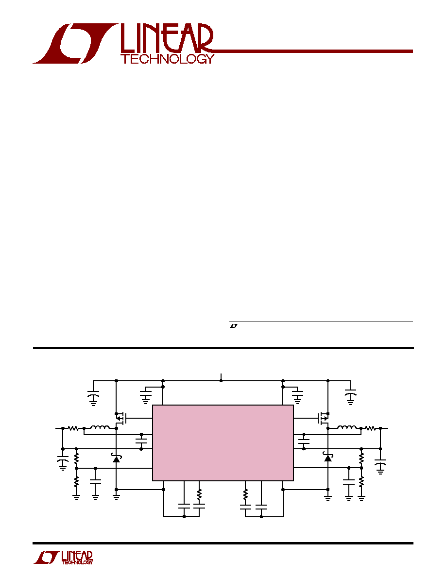
Figure 1. High Efficiency Dual 3.3V/2.5V Regulator
1000pF
100pF
+
+
+
1000pF
P-DRIVE 1
SENSE
+
1
SENSE
1
V
FB1
V
FB2
GND1
C
T1
I
TH1
I
TH2
C
T2
GND2
SENSE
2
SENSE
+
2
P-DRIVE 2
V
IN1
V
IN2
LTC1143L-ADJ
C
T2
300pF
3
2
14
15
7
6
11
R
C2
1k
C
C1
3300pF
C
C2
3300pF
C
T1
300pF
R
C1
1k
0.22
µ
F
13
5
12
9
8
10
4
1
16
V
OUT2
2.5V/2A
C
OUT2
220
µ
F
10V
×
2
R
SENSE2
0.05
P1B
L2
27
µ
H
D2
MBRS320T3
0.22
µ
F
C
IN2
22
µ
F
25V
×
2
C
IN1
22
µ
F
25V
×
2
P1A
D1
MBRS320T3
C
OUT1
220
µ
F
10V
×
2
L1
27
µ
H
R
SENSE1
0.05
R2
82.5k
1%
R1
49.9k
1%
V
OUT1
3.3V/2A
R3
49.9k
1%
R4
49.9k
1%
V
IN
4V TO 14V
1143 F01
+
L1, L2: SUMIDA CDRH125-270
P1: SILICONIX Si4953DY/FAIRCHILD NDS8947
R
SENSE1,
R
SENSE2
: DALE WSL-2010-.05
100pF
Burst Mode is a trademark of Linear Technology Corporation.
, LTC and LT are registered trademarks of Linear Technology Corporation.
Dual High Efficiency SO-16
Step-Down Switching Regulator
Controllers
TYPICAL APPLICATIO
N
U
APPLICATIO
N
S
U
s
Personal Digital Assistants
s
Notebook and Palmtop Computers
s
Battery-Operated Digital Devices
s
Portable Instruments
s
DC Power Distribution Systems

2
LTC1143/LTC1143L
LTC1143L-ADJ
ABSOLUTE
M
AXI
M
U
M
RATINGS
W
W
W
U
Input Supply Voltage (Pins 5,13) ............... 16V to 0.3V
Continuous Output Current (Pins 4,12) ................ 50mA
Sense Voltages (Pins 1, 8, 9, 16)
V
IN
12.7V .......................................... 13V to 0.3V
V
IN
< 12.7V .............................. (V
IN
+ 0.3V) to 0.3V
Shutdown Voltage
(LTC1143, LTC1143L, Pins 2, 10)...........7V to 0.3V
V
FB
Current (LTC1143L-ADJ, Pins 2, 10) ............... 1mA
Operating Temperature Range
Ambient .................................................. 0
°
C to 70
°
C
Extended Commercial (Note 4) ........... 40
°
C to 85
°
C
Junction Temperature (Note 1) ............................. 125
°
C
Storage Temperature Range .................. 65
°
C to 150
°
C
Lead Temperature (Soldering, 10 sec) .................. 300
°
C
PACKAGE/ORDER I
N
FOR
M
ATIO
N
W
U
U
ORDER PART
NUMBER
LTC1143CS
LTC1143LCS
ORDER PART
NUMBER
LTC1143LCS-ADJ
T
JMAX
= 125
°
C,
JA
= 95
°
C/W
ELECTRICAL CHARACTERISTICS
T
A
= 25
°
C, V
IN
= 10V unless otherwise noted.
Consult factory for Industrial and Military grade parts.
SYMBOL PARAMETER
CONDITIONS
MIN
TYP
MAX
UNITS
V
2
, V
10
Feedback Voltage (LTC1143L-ADJ)
V
IN
= 9V
q
1.21
1.25
1.29
V
I
2
, I
10
Feedback Current (LTC1143L-ADJ)
q
0.2
1
µ
A
V
OUT
Regulated Output Voltage (LTC1143/LTC1143L)
V
IN3,
V
IN5
= 9V, V
2
= V
10
= 0V
3.3V Output
I
LOAD
= 700mA
q
3.23
3.33
3.43
V
5V Output
I
LOAD
= 700mA
q
4.90
5.05
5.20
V
V
OUT
Output Voltage Line Regulation
V
IN
= 7V to 12V, I
LOAD
= 50mA
40
0
40
mV
Output Voltage Load Regulation
V
2
= V
10
= 0V
LTC1143/LTC1143L
3.3V Output
5mA < I
LOAD
< 2.0A
q
40
65
mV
5V Output
5mA < I
LOAD
< 2.0A
q
60
100
mV
Output Ripple (Burst Mode)
I
LOAD
= 0A
50
mV
P-P
I
5
, I
13
Input DC Supply Current (Note 2)
LTC1143:
Normal Mode
V
2
= V
10
= 0V, 4V < V
IN
< 12V
1.6
2.1
mA
Sleep Mode
V
2
= V
10
= 0V, 4V < V
IN3
< 12V, 6V < V
IN5
< 12V
160
230
µ
A
Shutdown
V
2
= V
10
= 2.1V, 4V < V
IN
< 12V
10
20
µ
A
LTC1143L:
Normal Mode
V
2
= V
10
= 0V, 3.5V < V
IN
< 12V
1.6
2.1
mA
Sleep Mode
V
2
= V
10
= 0V, 3.5V < V
IN3
< 12V, 6V < V
IN5
< 12V
160
230
µ
A
Shutdown
V
2
= V
10
= 2.1V, 3.5V < V
IN
< 12V
10
20
µ
A
LTC1143L-ADJ: Normal Mode
3.5V < V
IN
< 12V
1.6
2.1
mA
Sleep Mode
3.5V < V
IN
< 12V, V
OUT
3.3V
160
230
µ
A
TOP VIEW
S PACKAGE
16-LEAD PLASTIC SO
1
2
3
4
5
6
7
8
16
15
14
13
12
11
10
9
SENSE
+
1
V
FB1
GND1
P-DRIVE 1
V
IN2
C
T2
I
TH2
SENSE
2
SENSE
1
I
TH1
C
T1
V
IN1
P-DRIVE 2
GND2
V
FB2
SENSE
+
2
T
JMAX
= 125
°
C,
JA
= 95
°
C/W
TOP VIEW
S PACKAGE
16-LEAD PLASTIC SO
1
2
3
4
5
6
7
8
16
15
14
13
12
11
10
9
SENSE
+
3
SHUTDOWN 3
GND3
P-DRIVE 3
V
IN5
C
T5
I
TH5
SENSE
5
SENSE
3
I
TH3
C
T3
V
IN3
P-DRIVE 5
GND5
SHUTDOWN 5
SENSE
+
5

3
LTC1143/LTC1143L
LTC1143L-ADJ
ELECTRICAL CHARACTERISTICS
T
A
= 25
°
C, V
IN
= 10V unless otherwise noted.
SYMBOL
PARAMETER
CONDITIONS
MIN
TYP
MAX
UNITS
V
1
to V
16
,
Current Sense Threshold Voltage
V
8
to V
9
LTC1143/LTC1143L
V
2
= V
10
= 0V
V
SENSE
= V
OUT
+ 100mV (Forced)
25
mV
V
SENSE
= V
OUT
100mV (Forced)
q
130
150
170
mV
LTC1143L-ADJ
V
SENSE
= 5V, V
FB
= V
OUT
/4 + 25mV (Forced)
25
mV
V
SENSE
= 5V, V
FB
= V
OUT
/4 25mV (Forced)
q
130
150
170
mV
V
2
, V
10
Shutdown Pin Threshold
0.5
0.8
2
V
LTC1143/LTC1143L
I
2
, I
10
Shutdown Pin Input Current
0V < V
SHUTDOWN
= < 8V, V
IN3,
V
IN5
= 16V
1.2
5
µ
A
LTC1143/LTC1143L
I
6
, I
14
C
T
Pin Discharge Current
V
OUT
in Regulation, V
SENSE-
= V
OUT
50
70
90
µ
A
V
OUT
= 0V
2
10
µ
A
t
OFF
Off-Time (Note 3)
C
T
= 390pF, I
LOAD
= 700mA
4
5
6
µ
s
t
r
, t
f
Driver Output Transition Times
C
L
= 3000pF (Pins 4, 12), V
IN
= 6V
100
200
ns
40
°
C
T
A
85
°
C (Note 4), V
IN
= 10V unless otherwise noted.
V
2
, V
10
Feedback Voltage (LTC1143L-ADJ)
V
IN
= 9V
1.20
1.25
1.30
V
V
OUT
Regulated Output Voltage
V
IN3,
V
IN5
= 9V
LTC1143/LTC1143L
3.3V Output
I
LOAD
= 700mA
3.17
3.33
3.43
V
5V Output
I
LOAD
= 700mA
4.85
5.05
5.20
V
I
5
, I
13
Input DC Supply Current (Note 2)
LTC1143:
Normal Mode
V
2
= V
10
= 0V, 4V < V
IN
< 12V
1.6
2.4
mA
Sleep Mode
V
2
= V
10
= 0V, 4V < V
IN3
< 12V, 6V < V
IN5
< 12V
160
260
µ
A
Shutdown
V
2
= V
10
= 2.1V, 4V < V
IN
< 12V
10
22
µ
A
LTC1143L:
Normal Mode
V
2
= V
10
= 0V, 3.5V < V
IN
< 12V
1.6
2.4
mA
Sleep Mode
V
2
= V
10
= 0V, 3.5V < V
IN3
< 12V, 6V < V
IN5
< 12V
160
260
µ
A
Shutdown
V
2
= V
10
= 2.1V, 3.5V < V
IN
< 12V
10
22
µ
A
LTC1143L-ADJ: Normal Mode
3.5V < V
IN
< 12V
1.6
2.4
mA
Sleep Mode
3.5V < V
IN
< 12V, V
OUT
3.3V
160
260
µ
A
V
1
to V
16
,
Current Sense Threshold Voltage
V
8
to V
9
LTC1143/LTC1143L
V
2
= V
10
= 0V
V
SENSE
= V
OUT
+ 100mV (Forced)
25
mV
V
SENSE
= V
OUT
100mV (Forced)
125
150
185
mV
LTC1143L-ADJ
V
SENSE
= 5V, V
FB
= V
OUT
/4 + 25mV (Forced)
25
mV
V
SENSE
= 5V, V
FB
= V
OUT
/4 25mV (Forced)
125
150
185
mV
V
2
, V
10
Shutdown Pin Threshold
0.55
0.8
2
V
LTC1143/LTC1143L
The
q
denotes specifications which apply over the specified temperature
range.
Note 1: T
J
is calculated from the ambient temperature T
A
and power
dissipation P
D
according to the following formula:
LTC1143 series: T
J
= T
A
+ (P
D
· 125
°
C/W)
Note 2: This supply current is for one regulator block. Total supply
current is the sum of Pin 5 and Pin 13 currents. Dynamic supply current
is higher due to the gate charge being delivered at the switching
frequency. See Applications Information.
Note 3: In applications where R
SENSE
is placed at ground potential, the
off-time increases approximately 40%.
Note 4: The LTC1143 series is guaranteed to meet specified performance
from 0
°
C to 70
°
C and is designed, characterized and expected to meet
these extended temperature limits, but is not tested at 40
°
C to 85
°
C.

4
LTC1143/LTC1143L
LTC1143L-ADJ
TYPICAL PERFOR
M
A
N
CE CHARACTERISTICS
U
W
LOAD CURRENT (mA)
EFFICIENCY (%)
LTC1143 G02
1
70
90
95
100
10
100
1000
85
80
75
V
IN
= 5V
V
IN
= 10V
5V Output Efficiency
3.3V Output Efficiency
5V Efficiency vs Input Voltage
3.3V Efficiency vs Input Voltage
Load Regulation
Line Regulation
DC Supply Current
Supply Current in Shutdown
Operating Frequency vs V
IN
V
OUT
INPUT VOLTAGE (V)
0
EFFICIENCY (%)
100
98
96
94
92
90
88
86
84
82
80
4
8
1143 G03
12
16
I
LOAD
= 100mA
V
OUT
= 5V
I
LOAD
= 1A
LOAD CURRENT (mA)
EFFICIENCY (%)
LTC1143 G01
1
70
90
95
100
10
100
1000
85
80
75
V
IN
= 6V
V
IN
= 10V
INPUT VOLTAGE (V)
0
EFFICIENCY (%)
100
98
96
94
92
90
88
86
84
82
80
16
LTC1143 G04
4
8
12
V
OUT
= 3.3V
I
LOAD
= 1A
I
LOAD
= 100mA
INPUT VOLTAGE (V)
0
V
OUT
(mV)
40
30
20
10
0
10
20
30
40
16
LTC1143 G05
4
8
12
V
OUT
= 5V
I
LOAD
= 1A
LOAD CURRENT (A)
0
V
OUT
(mV)
20
0
20
40
60
80
100
2.0
LTC1143 G06
0.5
1.0
1.5
2.5
R
SENSE
= 0.05
V
IN
= 6V
V
IN
= 6V
V
IN
= 12V
V
OUT
= 5V
V
OUT
= 3.3V
V
IN
= 12V
INPUT VOLTAGE (V)
0
0
SUPPLY CURRENT (mA)
0.3
0.9
1.2
1.5
4
LTC1143 · G07
0.6
2
6
1.8
2.1
8
10
12
14
16
18
NOT INCLUDING
GATE CHARGE CURRENT
SLEEP MODE
ACTIVE MODE
PINS 5, 13
PER REGULATOR BLOCK
INPUT VOLTAGE (V)
0
SUPPLY CURRENT (
µ
A)
20
18
16
14
12
10
8
6
4
2
0
2
10
14
LTC1143 G08
8
18
4
6
12
16
PER LTC1143/LTC1143L
REGULATOR BLOCK
PINS 5, 13
V
SHUTDOWN
= 2V
(V
IN
V
OUT
) VOLTAGE (V)
0
NORMALIZED FREQUENCY
12
LTC1143 G09
2
6
8
1.6
1.4
1.2
1.0
0.8
0.6
0.4
0.2
0
4
10
V
OUT
= 5V
70°C
0°C
25°C

5
LTC1143/LTC1143L
LTC1143L-ADJ
TYPICAL PERFOR
M
A
N
CE CHARACTERISTICS
U
W
Gate Charge Supply Current
OPERATING FREQUENCY (kHz)
20
GATE CHARGE CURRENT (mA)
140
14
12
10
8
6
4
2
0
LTC1143 G10
80
260
200
Q
P
= 100nC
Q
P
= 29nC
Current Sense Threshold Voltage
TEMPERATURE (°C)
0
SENSE VOLTAGE (mV)
175
150
125
100
75
50
25
0
80
LTC1143 G12
20
40
60
100
MAXIMUM
THRESHOLD
MINIMUM
THRESHOLD
OUTPUT VOLTAGE (V)
0
OFF-TIME (
µ
s)
80
70
60
50
40
30
20
10
0
4
LTC1143 G11
1
2
3
5
V
SENSE
= V
OUT
V
OUT
= 5V
V
OUT
= 3.3V
Off-Time vs V
OUT
I
TH5
(Pin 7): Gain Amplifier Decoupling Point, 5V Section.
The 5V section current comparator threshold increases
with the Pin 7 voltage.
SENSE
5 (Pin 8): Connects to internal resistive divider
which sets the output voltage for the 5V section. Pin 8 is
also the () input for the current comparator on the 5V
section.
SENSE
+
5 (Pin 9): The (+) Input to the 5V Section Current
Comparator. A built-in offset between Pins 9 and 8 in
conjunction with R
SENSE 5
sets the current trip threshold
for the 5V section.
SHUTDOWN 5 (Pin 10): When grounded, the 5V section
operates normally. Pulling Pin 10 high holds the 5V section
MOSFET off and puts the 5V section in micropower shut-
down mode. Requires CMOS logic level signal with t
r
, t
f
< 1
µ
s.
Do not "float" Pin 10.
GND5 (Pin 11): 5V Section Ground. Two independent
ground lines must be routed separately from other grounds
to: 1) the () terminal of the 5V section output capacitor
and 2) the cathode of the Schottky diode D2 and ()
terminal of C
IN5
(see Figure 9).
P-DRIVE 5 (Pin 12): High Current Drive for Top P-Channel
MOSFET, 5V Section. Voltage swing at this pin is from
V
IN5
to ground.
PI
N
FU
N
CTIO
N
S
U
U
U
LTC1143/LTC1143L
SENSE
+
3 (Pin 1): The (+) Input to the 3.3V Section Current
Comparator. A built-in offset between Pins 1 and 16 in
conjunction with R
SENSE 3
sets the current trip threshold
for the 3.3V section.
SHUTDOWN 3 (Pin 2): When grounded, the 3.3V section
operates normally. Pulling Pin 2 high holds the MOSFET
off and puts the 3.3V section in micropower shutdown
mode. Requires CMOS logic level signal with t
r
, t
f
< 1
µ
s.
Do not "float" Pin 2.
GND3 (Pin 3): 3.3V Section Ground. Two independent
ground lines must be routed separately from other grounds
to: 1) the () terminal of the 3.3V section output capacitor
and 2) the cathode of the Schottky diode D1 and ()
terminal of C
IN3
(see Figure 9).
P-DRIVE 3 (Pin 4): High Current Drive for Top P-Channel
MOSFET, 3.3V Section. Voltage swing at this pin is from
V
IN3
to ground.
V
IN5
(Pin 5): Supply Pin, 5V Section. Must be closely
decoupled to 5V power ground Pin 11.
C
T5
(Pin 6): External capacitor C
T5
from Pin 6 to ground sets
the operating frequency for the 5V section. (The actual
frequency is also dependent upon the input voltage.)