1
LTC1147-3.3
LTC1147-5/LTC1147L
High Efficiency Step-Down
Switching Regulator Controllers
Figure 1. High Efficiency Step-Down Converter
U
A
O
PPLICATI
TYPICAL
, LTC and LT are registered trademarks of Linear Technology Corporation.
0V = NORMAL
>1.5V = SHUTDOWN
P-CHANNEL
Si4431DY
+
1
µ
F
L*
50
µ
H
R
SENSE
**
0.05
V
OUT
5V/2A
+
C
IN
100
µ
F
V
IN
(5.2V TO 14V)
I
TH
C
T
C
T
470pF
C
C
3300pF
R
C
1k
+
C
OUT
390
µ
F
D1
MBRD330
LT1147 ∑ F01
GND
V
IN
PDRIVE
LTC1147-5
SHDN
SENSE
+
SENSE
≠
1000pF
COILTRONICS CTX50-2-MP
KRL SL-1-C1-0R050J
*
**
LOAD CURRENT (A)
0.001
70
EFFICIENCY (%)
90
95
100
0.01
0.1
1
LT1147 ∑ TA01
85
80
75
V
IN
= 6V
V
IN
= 10V
LTC1147-5 Efficiency
s
Very High Efficiency: Over 95% Possible
s
Wide V
IN
Range: 3.5V* to 16V
s
Current Mode Operation for Excellent Line and Load
Transient Response
s
High Efficiency Maintained Over Three Decades of
Output Current
s
Low 160
µ
A Standby Current at Light Loads
s
Logic Controlled Micropower Shutdown: I
Q
< 20
µ
A
s
Short-Circuit Protection
s
Very Low Dropout Operation: 100% Duty Cycle
s
High Efficiency in a Small Amount of Board Space
s
Output Can Be Externally Held High in Shutdown
s
Available in 8-Pin SO Package
The LTC
Æ
1147 series are step-down switching regulator
controllers featuring automatic Burst Mode
TM
operation to
maintain high efficiencies at low output currents. These
devices drive an external P-channel power MOSFET at
switching frequencies exceeding 400kHz using a constant
off-time current mode architecture providing constant
ripple current in the inductor.
The operating current level is user-programmable via an
external current sense resistor. Wide input supply range
allows operation from 3.5V* to 14V (16V maximum).
Constant off-time architecture provides low dropout regu-
lation limited by only the R
DS(ON)
of the external MOSFET
and resistance of the inductor and current sense resistor.
The LTC1147 series incorporates automatic power saving
Burst Mode
operation to reduce switching losses when
load currents drop below the level required for continuous
operation. Standby power is reduced to only 2mW at
V
IN
= 10V (at I
OUT
= 0). Load currents in Burst Mode
operation are typically 0mA to 300mA.
For applications where even higher efficiency is required,
refer to the LTC1148 data sheet and Application Note 54.
Burst Mode
is a trademark of Linear Technology Corporation.
*LTC1147L and LTC1147L-3.3 only.
FEATURES
DESCRIPTIO
U
APPLICATIO S
U
s
Notebook and Palmtop Computers
s
Portable Instruments
s
Battery-Operated Digital Devices
s
Cellular Telephones
s
DC Power Distribution Systems
s
GPS Systems
2
LTC1147-3.3
LTC1147-5/LTC1147L
Input Supply Voltage (Pin 1)..................... 16V to ≠ 0.3V
Continuous Output Current (Pin 8) ...................... 50mA
Sense Voltages (Pins 4, 5)
V
IN
12.7V ...........................................13V to ≠ 0.3V
V
IN
< 12.7V ............................... (V
IN
+ 0.3V) to ≠ 0.3V
ABSOLUTE AXI U
RATI GS
W
W
W
U
Operating Ambient Temperature Range
LTC1147C................................................ 0
∞
C to 70
∞
C
LTC1147I ............................................. ≠40
∞
C to 85
∞
C
Extended Commercial
Temperature Range (Note 4) ................. ≠ 40
∞
C to 85
∞
C
Junction Temperature (Note 1)............................ 125
∞
C
Storage Temperature Range ................ ≠ 65
∞
C to 150
∞
C
Lead Temperature (Soldering, 10 sec)................. 300
∞
C
SYMBOL
PARAMETER
CONDITIONS
MIN
TYP
MAX
UNITS
V
6
Feedback Voltage (LTC1147L)
V
IN
= 9V
q
1.21
1.25
1.29
V
I
6
Feedback Current (LTC1147L)
q
0.2
1
µ
A
V
OUT
Regulated Output Voltage
V
IN
= 9V
LTC1147-3.3, LTC1147L-3.3
I
LOAD
= 700mA
q
3.23
3.33
3.43
V
LTC1147-5
I
LOAD
= 700mA
q
4.90
5.05
5.20
V
V
OUT
Output Voltage Line Regulation
V
IN
= 7V to 12V, I
LOAD
= 50mA
≠ 40
0
40
mV
Output Voltage Load Regulation
LTC1147-3.3, LTC1147L-3.3
5mA < I
LOAD
< 2A
q
40
65
mV
LTC1147-5
5mA < I
LOAD
< 2A
q
60
100
mV
Burst Mode Output Ripple
I
LOAD
= 0A
50
mV
P-P
I
Q
Input DC Supply Current (Note 2)
(Note 5)
LTC1147 Series
Normal Mode
4V < V
IN
< 12V
1.6
2.1
mA
Sleep Mode
4V < V
IN
< 12V
160
230
µ
A
Sleep Mode (LTC1147-5)
5V < V
IN
< 12V
160
230
µ
A
Shutdown
V
SHDN
= 2.1V, 4V < V
IN
< 12V
10
20
µ
A
LTC1147L Series
Normal Mode
3.5V < V
IN
< 12V
1.6
2.1
mA
Sleep Mode
3.5V < V
IN
< 12V
160
230
µ
A
Shutdown (LTC1147L-3.3)
V
SHDN
= 2.1V, 3.5V < V
IN
< 12V
10
20
µ
A
T
A
= 25
∞
C, V
IN
= 10V, V
SHDN
= 0V, unless otherwise noted.
ELECTRICAL CHARACTERISTICS
Consult factory for Military grade parts.
PACKAGE/ORDER I FOR ATIO
U
U
W
* ADJUSTABLE OUTPUT VERSION
SHDN
(V
FB
*)
1
2
3
4
8
7
6
5
TOP VIEW
V
IN
C
T
I
TH
SENSE
≠
PDRIVE
GND
SENSE
+
N8 PACKAGE
8-LEAD PLASTIC DIP
S8 PACKAGE
8-LEAD PLASTIC SO
T
JMAX
= 125
∞
C,
JA
= 110
∞
C/W (N)
T
JMAX
= 125
∞
C,
JA
= 150
∞
C/W (S)
LTC1147LCS8
LTC1147LCS8-3.3
LTC1147LIS8
11473
11475
1147L
1147L3
1147LI
1147I3
LTC1147CN8-3.3
LTC1147CN8-5
LTC1147CS8-3.3
LTC1147CS8-5
LTC1147IS8-3.3
ORDER PART NUMBER
S8 PART MARKING
3
LTC1147-3.3
LTC1147-5/LTC1147L
T
A
= 25
∞
C, V
IN
= 10V, V
SHDN
= 0V, unless otherwise noted.
ELECTRICAL CHARACTERISTICS
SYMBOL
PARAMETER
CONDITIONS
MIN
TYP
MAX
UNITS
V
5
≠ V
4
Current Sense Threshold Voltage (Note 6)
LTC1147-3.3, LTC1147L-3.3
V
SENSE
≠
= V
OUT
+ 100mV (Forced)
25
mV
V
SENSE
≠
= V
OUT
≠ 100mV (Forced)
130
150
170
mV
LTC1147≠5
V
SENSE
≠
= V
OUT
+ 100mV (Forced)
25
mV
V
SENSE
≠
= V
OUT
≠ 100mV (Forced)
130
150
170
mV
LTC1147L
V
SENSE
≠
= 5V, V6 = V
OUT
/4 + 25mV (Forced)
25
mV
V
SENSE
≠
= 5V, V6 = V
OUT
/4 ≠ 25mV (Forced)
130
150
170
mV
V
6
SHDN Pin Threshold
LTC1147-3.3/LTC1147-5/LTC1147L-3.3
0.5
0.8
2
V
I
6
SHDN Pin Input Current
LTC1147-3.3/LTC1147-5/LTC1147L-3.3
0V < V
SHDN
< 8V, V
IN
= 16V
1.2
5
µ
A
I
2
C
T
Pin Discharge Current
V
OUT
in Regulation, V
SENSE
≠
= V
OUT
50
70
90
µ
A
V
OUT
= 0V
2
10
µ
A
t
OFF
Off-Time (Note 3)
C
T
= 390pF, I
LOAD
= 700mA
4
5
6
µ
s
t
r
, t
f
Driver Output Transition Times
C
L
= 3000pF (Pin 8), V
IN
= 6V
100
200
ns
SYMBOL
PARAMETER
CONDITIONS
MIN
TYP
MAX
UNITS
V
6
Feedback Voltage (LTC1147L)
V
IN
= 9V
q
1.20
1.25
1.30
V
V
OUT
Regulated Output Voltage
V
IN
= 9V
LTC1147-3.3/LTC1147L-3.3
I
LOAD
= 700mA
q
3.17
3.33
3.43
V
LTC1147-5
I
LOAD
= 700mA
q
4.85
5.05
5.20
V
I
Q
Input DC Supply Current (Note 2)
(Note 5)
LTC1147 Series
Normal Mode
4V < V
IN
< 12V
1.6
2.4
mA
Sleep Mode
4V < V
IN
< 12V
160
260
µ
A
Sleep Mode (LTC1147-5)
5V < V
IN
< 12V
160
260
µ
A
Shutdown
V
SHDN
= 2.1V, 4V < V
IN
< 12V
10
22
µ
A
LTC1147L Series
Normal Mode
3.5V < V
IN
< 12V
1.6
2.4
mA
Sleep Mode
3.5V < V
IN
< 12V
160
260
µ
A
Shutdown (LTC1147L-3.3)
V
SHDN
= 2.1V, 3.5V < V
IN
< 12V
10
22
µ
A
V
5
≠ V
4
Current Sense Threshold Voltage (Note 6)
LTC1147-3.3
V
SENSE
≠
= V
OUT
+ 100mV (Forced)
25
mV
V
SENSE
≠
= V
OUT
≠ 100mV (Forced)
q
125
150
185
mV
LTC1147-5
V
SENSE
≠
= V
OUT
+ 100mV (Forced)
25
mV
V
SENSE
≠
= V
OUT
≠ 100mV (Forced)
q
125
150
185
mV
LTC1147L
V
SENSE
≠
= 5V, 6V = V
OUT
/4 + 25mV (Forced)
25
mV
V
SENSE
≠
= 5V, 6V = V
OUT
/4 ≠ 25mV (Forced)
125
150
185
mV
V
6
SHDN Pin Threshold
LTC1147-3.3/LTC1147-5/LTC1147L-3.3
0V < V
SHDN
< 8V, V
IN
= 16V
0.5
0.8
2
V
t
OFF
Off-Time (Note 3)
C
T
= 390pF, I
LOAD
= 700mA
3.8
5
6.5
µ
s
The
q
denotes specifications which apply over the full specified
temperature range.
Note 1: T
J
is calculated from the ambient temperature T
A
and power
dissipation P
D
according to the following formulas:
LTC1147CN8-3.3/LTC1147CN8-5: T
J
= T
A
+ (P
D
)(110
∞
C/W)
LTC1147LIS/LTC1147IS8/LTC1147LCS/
LTC1147CS8-3.3/LTC1147CS8-5: T
J
= T
A
+ (P
D
)(150
∞
C/W)
Note 2: Dynamic supply current is higher due to the gate charge being
delivered at the switching frequency. See Applications Information.
Note 3: In applications where R
SENSE
is placed at ground potential, the off-
time increases approximately 40%.
Note 4: The LTC1147C is guaranteed to meet specified performance from
0
∞
C to 70
∞
C and is designed, characterized and expected to meet these
extended temperature limits, but is not tested at ≠ 40
∞
C and 85
∞
C. The
LTC1147I is guaranteed to meet the extended temperature limits.
Note 5: The LTC1147L/LTC1147L-3.3 allow operation to V
IN
= 3.5V.
Note 6: The LTC1147L is tested with external feedback resistors resulting
in a nominal output voltage of 2.5V.
≠ 40
∞
C
T
A
85
∞
C (Note 4), V
IN
= 10V, unless otherwise noted.
4
LTC1147-3.3
LTC1147-5/LTC1147L
LOAD CURRENT (A)
0
≠100
V
OUT
(mV)
≠80
≠60
≠40
≠20
0
20
0.5
1.0
1.5
2.0
LTC1147 ∑ G03
2.5
FIGURE 1 CIRCUIT
R
SENSE
= 0.05
V
IN
= 6V
V
IN
= 12V
INPUT VOLTAGE (V)
0
V
OUT
(mV)
0
10
20
16
LTC1147 ∑ G02
≠10
≠20
≠40
4
8
12
≠30
40
30
FIGURE 1 CIRCUIT
I
LOAD
= 1A
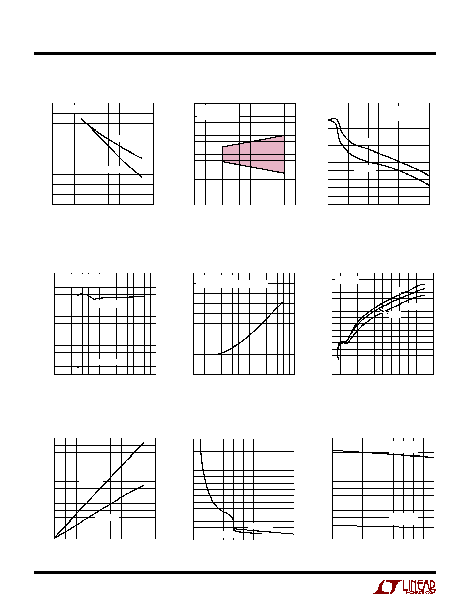
Efficiency vs Input Voltage
Line Regulation
Load Regulation
INPUT VOLTAGE (V)
0
80
EFFICIENCY (%)
82
86
88
90
100
94
4
8
LTC1147 ∑ G01
84
96
98
92
12
16
FIGURE 1 CIRCUIT
I
LOAD
= 1A
I
LOAD
= 100mA
OPERATING FREQUENCY (kHz)
20
0
GATE CHARGE CURRENT (mA)
2
4
6
14
10
80
140
12
8
200
260
Q
P
= 29nC
Q
P
= 50nC
LTC1147 ∑ G07
TEMPERATURE (
∞
C)
0
0
SENSE VOLTAGE (mV)
25
50
75
175
125
20
40
150
100
60
80
100
MAXIMUM
THRESHOLD
MINIMUM
THRESHOLD
LTC1147 ∑ G09
OUTPUT VOLTAGE (V)
0
OFF-TIME (
µ
s)
40
50
60
4
LTC1147 ∑ G08
30
20
0
1
2
3
10
80
70
5
LTC1147-5
LTC1147-3.3
V
SENSE
≠
= V
OUT
Gate Charge Supply Current
Operating Frequency
vs (V
IN
≠ V
OUT
)
INPUT VOLTAGE (V)
0
0
SUPPLY CURRENT (mA)
0.3
0.9
1.2
1.5
4
LTC1147 ∑ G04
0.6
2
6
1.8
2.1
8
10
12
14
16
18
NOT INCLUDING
GATE CHARGE CURRENT
SLEEP MODE
ACTIVE MODE
(V
IN
≠ V
OUT
) VOLTAGE (V)
0
NORMALIZED FREQUENCY
0.6
1.0
8
LTC1148 ∑ G06
0.4
0
2
4
6
0.2
1.2
0.8
10
12
1.4
1.6
V
OUT
= 5V
0
∞
C
70
∞
C
25
∞
C
INPUT VOLTAGE (V)
0
0
SUPPLY CURRENT (
µ
A)
2
6
8
10
20
14
4
8
10
18
LTC1147 ∑ G05
4
16
18
12
2
6
12
14
16
V
SHUTDOWN
= 2V
(NOT AVAILABLE ON LTC1147L)
DC Supply Current
Supply Current in Shutdown
Current Sense Threshold Voltage
Off-Time vs V
OUT
TYPICAL PERFOR A CE CHARACTERISTICS
U
W
5
LTC1147-3.3
LTC1147-5/LTC1147L
V
IN
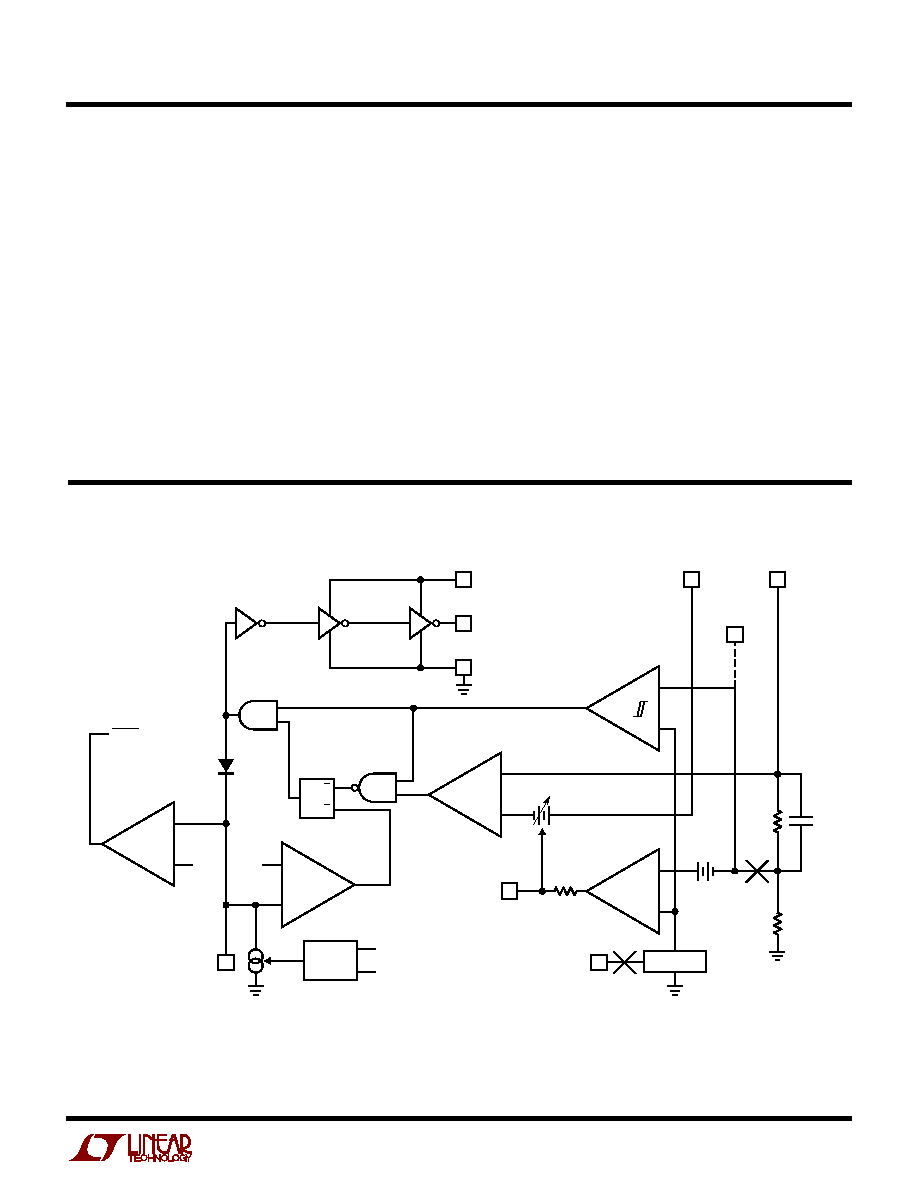
(Pin 1): Main Supply Pin. Must be closely decoupled
to ground Pin 7.
C
T
(Pin 2): External capacitor C
T
from Pin 2 to ground sets
the operating frequency. The actual frequency is also
dependent upon the input voltage.
I
TH
(Pin 3): Gain Amplifier Decoupling Point. The current
comparator threshold increases with the Pin 3 voltage.
SENSE
≠
(Pin 4): Connects to internal resistive divider
which sets the output voltage. Pin 4 is also the (≠) input for
the current comparator.
SENSE
+
(Pin 5): The (+) input to the current comparator.
A built-in offset between Pins 4 and 5 in conjunction with
R
SENSE
sets the current trip threshold.
SHDN/V
FB
(Pin 6): When grounded, the fixed output
versions of the LTC1147 family operate normally. Pulling
Pin 6 high holds the P-channel MOSFET off and puts the
LTC1147 in micropower shutdown mode. Requires CMOS
logic signal with t
r
, t
f
< 1
µ
s. Do not leave this pin floating.
On the LTC1147L this pin serves as the feedback pin from
an external resistive divider used to set the output voltage.
GND (Pin 7): Two independent ground lines must be
routed separately to: 1) the (≠) terminal of C
OUT
, and 2) the
cathode of the Schottky diode and (≠) terminal of C
IN
.
PDRIVE (Pin 8): High current drive for the P-channel
MOSFET. Voltage swing at this pin is from V
IN
to ground.
Pin 6 Connection Shown For LTC1147-3.3 and LTC1147-5; Changes Create LTC1147L.
+
≠
1
PDRIVE
V
IN
GND
R
S
Q
≠
+
C
25mV TO 150mV
3
13k
I
TH
1.25V
6
REFERENCE
≠
+
SHDN
V
OS
≠
+
V
G
5
6
SENSE
+
100k
5pF
≠
+
V
TH1
T
≠
+
V
TH2
S
SLEEP
2
C
T
OFF-TIME
CONTROL
V
IN
SENSE
≠
SENSE
≠
4
8
7
LTC1147 ∑ FD
V
FB
PI FU CTIO S
U
U
U
FU CTIO AL DIAGRA
U
U
W