 | –≠–ª–µ–∫—Ç—Ä–æ–Ω–Ω—ã–π –∫–æ–º–ø–æ–Ω–µ–Ω—Ç: LTC1149CS | –°–∫–∞—á–∞—Ç—å:  PDF PDF  ZIP ZIP |
1
LTC1149
LTC1149-3.3/LTC1149-5
S
FEATURE
D
U
ESCRIPTIO
s
Operation to 48V Input Voltage
s
Ultrahigh Efficiency: Up to 95%
s
Current Mode Operation for Excellent Line and
Load Transient Response
s
High Efficiency Maintained over Wide Current Range
s
Logic-Controlled Micropower Shutdown
s
Short-Circuit Protection
s
Very Low Dropout Operation: 100% Duty Cycle
s
Synchronous FET Switching for High Efficiency
s
Adaptive Nonoverlap Gate Drives
s
Available in 16-Pin Narrow SO Package
The LTC
Æ
1149 series is a family of synchronous step-
down switching regulator controllers featuring automatic
Burst Mode
TM
operation to maintain high efficiencies at
low output currents. These devices drive external comple-
mentary power MOSFETs at switching frequencies up
to 250kHz using a constant off-time current-mode archi-
tecture.
Special onboard regulation and level-shift circuitry allow
operation at input voltages from dropout to 48V (60V
absolute max). The constant off-time architecture main-
tains constant ripple current in the inductor, easing the
design of wide input range converters. Current mode
operation provides excellent line and load transient
response. The operating current level is user-program-
mable via an external current sense resistor.
The LTC1149 series incorporates automatic power saving
Burst Mode
operation when load currents drop below the
level required for continuous operation. Standby power is
reduced to only about 8mW at V
IN
= 12V. In shutdown,
both MOSFETs are turned off.
High Efficiency Synchronous
Step-Down Switching Regulators
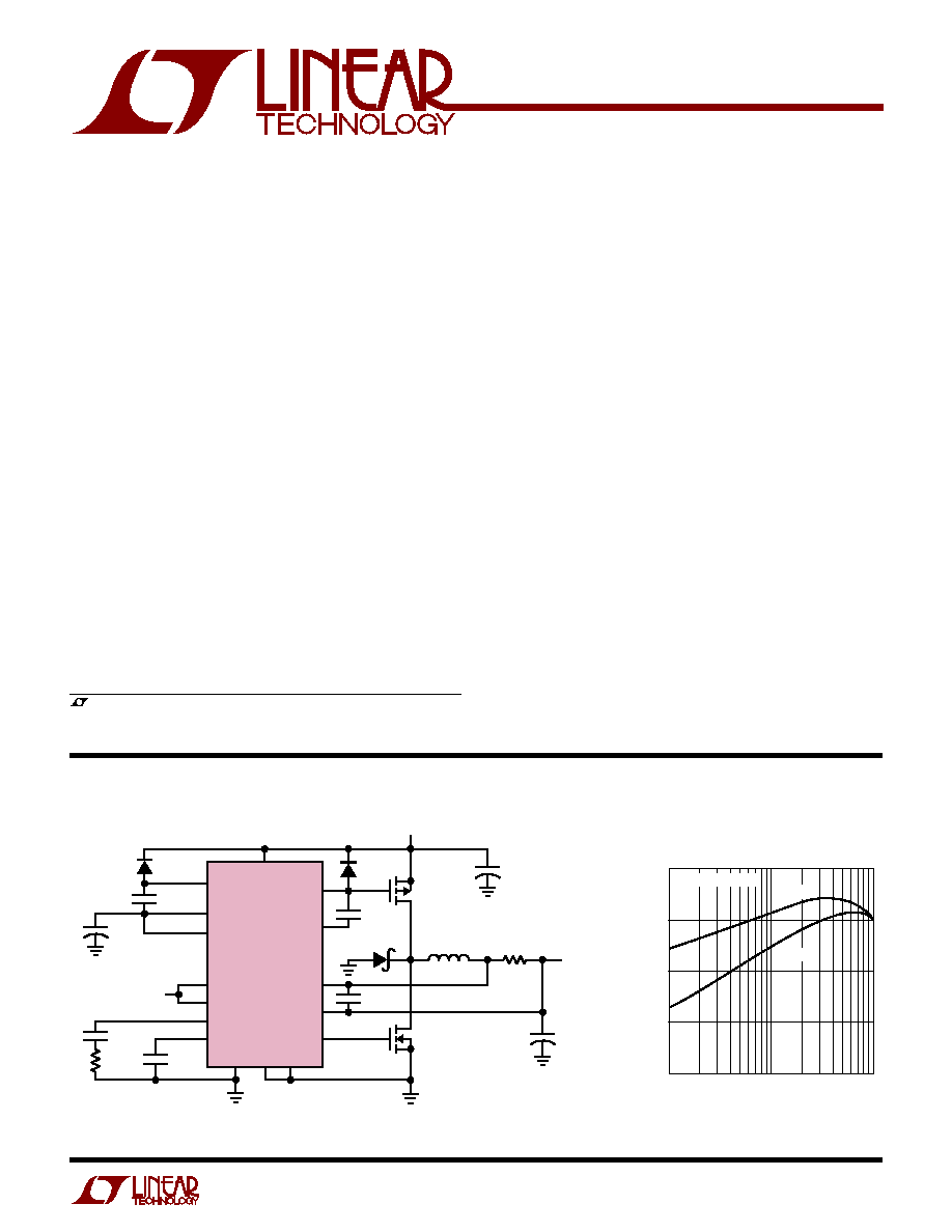
Figure 1. High Efficiency Step-Down Regulator
U
A
O
PPLICATI
TYPICAL
0.068
µ
F
V
IN
CAP
PDRIVE
LTC1149-5
SHDN1
I
TH
C
T
SGND
PGATE
V
CC
V
CC
SHDN2
SENSE
≠
SENSE
+
P, RGNDS
NGATE
1000pF
N-CHANNEL
IRFR024
0.047
µ
F
1N4148
1N4148
V
IN
P-CHANNEL
IRFR9024
D1
1N5819
L*
62
µ
H
R
SENSE
**
0.05
V
OUT
5V/2A
C
OUT
220
µ
F
C
IN
100
µ
F
100V
3.3
µ
F
0V = NORMAL
>2V = SHUTDOWN
3300
µ
F
C
T
470pF
1k
1149 F01
*COILTRONICS CTX62-2-MP
**KRL SL-1-C1-0R050J
+
+
+
LOAD CURRENT (A)
0.02
60
EFFICIENCY (%)
70
80
100
0.2
2
1149 TA01
90
V
IN
= 12V
V
IN
= 24V
FIGURE 1 CIRCUIT
LTC1149-5 Efficiency
s
Notebook and Palmtop Computers
s
Portable Instruments
s
Battery-Operated Digital Devices
s
Industrial Power Distribution
s
Avionics Systems
s
Telecom Power Supplies
U
S
A
O
PPLICATI
, LTC and LT are registered trademarks of Linear Technology Corporation.
Burst Mode
is a trademark of Linear Technology Corporation.
2
LTC1149
LTC1149-3.3/LTC1149-5
A
U
G
W
A
W
U
W
A
R
BSOLUTE
XI
TI
S
W
U
U
PACKAGE/ORDER I FOR ATIO
Input Supply Voltage (Pin 2)...................... ≠ 15V to 60V
V
CC
Output Current (Pin 3) .................................. 50mA
V
CC
Input Voltage (Pin 5) ........................................ 16V
Continuous Output Current (Pins 4, 13) .............. 50mA
Sense Voltages (Pins 8, 9)
V
IN
12.7V .......................................... 13V to ≠ 0.3V
V
IN
< 12.7V ............................. (V
CC
+ 0.3V) to ≠ 0.3V
Shutdown Voltages (Pins 10, 15) ............................. 7V
Operating Temperature Range .................... 0
∞
C to 70
∞
C
Extended Commercial
Temperature Range ............................... ≠ 40
∞
C to 85
∞
C
Junction Temperature (Note 1) ............................ 125
∞
C
Storage Temperature Range ................ ≠ 65
∞
C to 150
∞
C
Lead Temperature (Soldering, 10 sec)................. 300
∞
C
ELECTRICAL C
C
HARA TERISTICS
T
A
= 25
∞
C, V
IN
= 12V, V
10
= 0V (Note 2), unless otherwise noted.
SYMBOL
PARAMETER
CONDITIONS
MIN
TYP
MAX
UNITS
V
10
Feedback Voltage (LTC1149 Only)
V
IN
= 9V
q
1.21
1.25
1.29
V
I
10
Feedback Current (LTC1149 Only)
q
0.2
1
µ
A
V
OUT
Regulated Output Voltage
V
IN
= 9V
LTC1149-3.3
I
LOAD
= 700mA
q
3.23
3.33
3.43
V
LTC1149-5
I
LOAD
= 700mA
q
4.9
5.05
5.2
V
V
OUT
Output Voltage Line Regulation
V
IN
= 9V to 48V, I
LOAD
= 50mA
≠ 40
0
40
mV
Output Voltage Load Regulation
LTC1149-3.3
5mA < I
LOAD
< 2A
q
40
65
mV
LTC1149-5
5mA < I
LOAD
< 2A
q
60
100
mV
Burst Mode
Output Ripple
I
LOAD
= 0A
50
mV
P-P
I
2
Input DC Supply Current (Note 3)
Normal Mode
V
IN
= 12V
2.0
2.8
mA
V
IN
= 48V
2.2
3.0
mA
Burst Mode
V
IN
= 12V
0.6
0.9
mA
V
IN
= 48V
0.8
1.1
mA
Shutdown
V
IN
= 12V, V
15
= 2V
135
170
µ
A
V
IN
= 48V, V
15
= 2V
300
390
µ
A
V
CC
Internal Regulator Voltage
V
IN
= 12V to 48V
q
9.75
10.25
11
V
(Sets MOSFET Gate Drive Levels)
I
3
= 20mA
V
2
≠ V
3
V
CC
Dropout Voltage
V
IN
= 5V, I
3
= 10mA
200
250
mV
V
IN
≠ V
1
P-Gate to Source Voltage (Off)
V
IN
= 12V
q
≠ 0.2
0
V
V
IN
= 48V
q
≠ 0.2
0
V
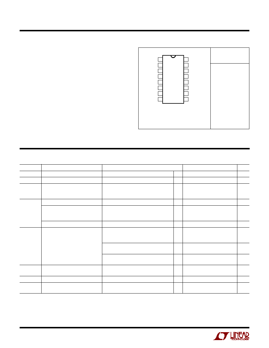
LTC1149CN
LTC1149CN-3.3
LTC1149CN-5
LTC1149CS
LTC1149CS-3.3
LTC1149CS-5
ORDER PART
NUMBER
Consult factory for Industrial and Military grade parts.
1
2
3
4
5
6
7
8
TOP VIEW
S PACKAGE
16-LEAD PLASTIC SO
N PACKAGE
16-LEAD PDIP
16
15
14
13
12
11
10
9
PGATE
V
IN
V
CC
PDRIVE
V
CC
C
T
I
TH
SENSE
≠
CAP
SHDN2
RGND
NGATE
PGND
SGND
SENSE
+
*FIXED OUTPUT VERSIONS
V
FB
/
SHDN1*
T
JMAX
= 125
∞
C,
JA
= 70
∞
C/ W (N)
T
JMAX
= 125
∞
C,
JA
= 110
∞
C/ W (S)
3
LTC1149
LTC1149-3.3/LTC1149-5
SYMBOL
PARAMETER
CONDITIONS
MIN
TYP
MAX
UNITS
V
9
≠ V
8
Current Sense Threshold Voltage
LTC1149
V
8
= 5V, V
10
= 1.32V (Forced)
25
mV
V
8
= V
OUT
≠ 100mV
q
130
150
170
mV
LTC1149-3.3
V
8
= 3.5V (Forced)
25
mV
V
8
= V
OUT
≠ 100mV
q
130
150
170
mV
LTC1149-5
V
8
= 5.3V (Forced)
25
mV
V
8
= V
OUT
≠ 100mV
q
130
150
170
mV
V
10
Shutdown 1 Threshold
LTC1149-3.3, LTC1149-5
0.5
0.8
2
V
V
15
Shutdown 2 Threshold
0.8
1.4
2
V
I
15
Shutdown 2 Input Current
V
15
= 5V
18
25
µ
A
I
6
C
T
Pin Discharge Current
V
OUT
In Regulation, V
SENSE
≠
= V
OUT
50
70
90
µ
A
V
OUT
= 0V
2
10
µ
A
t
OFF
Off-Time (Note 4)
C
T
= 390pF, I
LOAD
= 700mA
4
5
6
µ
s
t
r
, t
f
Driver Output Transition Times
C
L
= 3000pF (Pins 4, 13), V
IN
= 6V
100
200
ns
ELECTRICAL C
C
HARA TERISTICS
T
A
= 25
∞
C, V
IN
= 12V, V
10
= 0V (Note 2), unless otherwise noted.
≠ 40
∞
C
T
A
85
∞
C (Note 5), unless otherwise noted.
SYMBOL
PARAMETER
CONDITIONS
MIN
TYP
MAX
UNITS
V
10
Feedback Voltage LTC1149 Only
1.2
1.25
1.3
V
V
OUT
Regulated Output Voltage
V
IN
= 9V
LTC1149-3.3
I
LOAD
= 700mA
3.17
3.33
3.43
V
LTC1149-5
I
LOAD
= 700mA
4.85
5.05
5.2
V
I
2
Input DC Supply Current (Note 3)
Normal Mode
V
IN
= 12V
2.0
3.2
mA
V
IN
= 48V
2.2
3.5
mA
Burst Mode
V
IN
= 12V
0.6
1.05
mA
V
IN
= 48V
0.8
1.30
mA
Shutdown
V
IN
= 12V, V
15
= 2V
135
230
µ
A
V
IN
= 48V, V
15
= 2V
300
520
µ
A
V
CC
Internal Regulator Voltage
V
IN
= 12V to 48V
9.75
10.25
11
V
(Sets MOSFET Gate Drive Levels)
I
3
= 20mA
V
9
≠ V
8
Current Sense Threshold Voltage
Low Threshold (Forced)
25
mV
High Threshold (Forced)
125
150
175
mV
V
15
Shutdown 2 Threshold
0.8
1.4
2
V
t
OFF
Off-Time (Note 4)
C
T
= 390pF, I
LOAD
= 700mA, V
IN
= 10V
3.8
5
6
µ
s
The
q
denotes specifications which apply over the full operating
temperature range.
Note 1: T
J
is calculated from the ambient temperature T
A
and power
dissipation P
D
according to the following formulas:
LTC1149CN, LTC1149CN-3.3, LTC1149CN-5: T
J
= T
A
+ (P
D
)(70
∞
C/W)
LTC1149CS, LTC1149CS-3.3, LTC1149CS-5: T
J
= T
A
+ (P
D
)(110
∞
C/W)
Note 2: Pin 10 is a shutdown pin on the LTC1149-3.3 and LTC1149-5
fixed output voltage versions and must be at ground potential for testing.
Note 3: Dynamic supply current is higher due to the gate charge being
delivered at the switching frequency. The allowable operating frequency
may be limited by power dissipation at high input voltages. See Typical
Performance Characteristics and Applications Information.
Note 4: In applications where R
SENSE
is placed at ground potential, the off-
time increases approximately 40%.
Note 5: The LTC1149, LTC1149-3.3, and LTC1149-5 are not tested and
not quality assurance sampled at ≠ 40
∞
C and 85
∞
C. These specifications
are guaranteed by design and/or correlation.
4
LTC1149
LTC1149-3.3/LTC1149-5
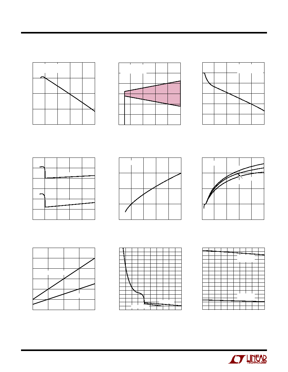
C
C
HARA TERISTICS
U
W
A
TYPICAL PERFOR
CE
Load Regulation
Efficiency vs Input Voltage
Line Regulation
Operating Frequency
vs (V
IN
≠ V
OUT
)
Gate Charge Supply Current
Current Sense Threshold Voltage
DC Supply Current
Supply Current in Shutdown
Off-Time vs V
OUT
LOAD CURRENT (A)
0
≠100
V
OUT
(mV)
≠80
≠60
≠40
≠20
0
20
0.5
1.0
1.5
2.0
1149 G03
2.5
FIGURE 1 CIRCUIT
V
IN
= 24V
OPERATING FREQUENCY (kHz)
50
0
GATE CHARGE CURRENT (mA)
5
10
15
20
25
30
100
150
200
250
1149 G07
Q
P
+ Q
N
= 100nC
Q
P
+ Q
N
= 50nC
OUTPUT VOLTAGE (V)
1
OFF-TIME (
µ
s)
40
50
60
5
1149 G08
30
20
0
2
3
4
10
80
70
0
LTC1149-5
LTC1149-3.3
TEMPERATURE (
∞
C)
20
SENSE VOLTAGE (mV)
80
100
120
100
1149 G09
60
40
0
40
60
80
20
160
140
0
MAXIMUM
THRESHOLD
MINIMUM
THRESHOLD
(V
IN
≠ V
OUT
) VOLTAGE (V)
0
NORMALIZED FREQUENCY
1.0
1.5
20
1149 G06
0.5
0
5
10
15
25
2.0
V
OUT
= 5V
T = 70
∞
C
T = 0
∞
C
T = 25
∞
C
INPUT VOLTAGE (V)
0
SUPPLY CURRENT (
µ
A)
200
300
40
1149 G05
100
0
10
20
30
50
400
V
SD2
= 2V
INPUT VOLTAGE (V)
0
0
SUPPLY CURRENT (mA)
0.5
1.0
1.5
2.0
2.5
3.0
10
20
30
40
1149 G04
50
ACTIVE MODE
SLEEP MODE
INPUT VOLTAGE (V)
0
≠60
V
OUT
(mV)
≠40
≠20
0
20
40
60
10
20
30
40
1149 G02
50
FIGURE 1 CIRCUIT
I
LOAD
= 1A
INPUT VOLTAGE (V)
0
EFFICIENCY (%)
90
95
40
1149 G01
85
80
10
20
30
50
100
FIGURE 1 CIRCUIT
I
LOAD
= 1A

5
LTC1149
LTC1149-3.3/LTC1149-5
PI FU CTIO S
U
U
U
PGATE (Pin 1): Level-Shifted Gate Drive Signal for Top
P-Channel MOSFET. The voltage swing at Pin 1 is from V
IN
to V
IN
≠ V
CC
.
V
IN
(Pin 2): Main Supply Input Pin.
V
CC
(Pin 3): Output Pin of Low Dropout 10V Regulator.
Pin
3 is not protected against DC short circuits.
PDRIVE (Pin 4): High Current Gate Drive for Top
P-Channel MOSFET. The voltage swing at Pin 4 is from V
CC
to ground.
V
CC
(Pin 5): Regulated 10V Input for Driver and Control
Supplies. Must be closely decoupled to power ground.
C
T
(Pin 6): External capacitor C
T
from Pin 6 to ground sets
the operating frequency. (The frequency is also dependent
on the ratio V
OUT
/V
IN
.)
I
TH
(Pin 7): Gain Amplifier Decoupling Point. The current
comparator threshold increases with the Pin 7 voltage.
SENSE
≠
(Pin 8): Connects to internal resistive divider
which sets the output voltage in LTC1149-3.3 and
LTC1149-5 versions. Pin 8 is also the (≠) input for the
current comparator.
SENSE
+
(Pin 9): The (+) Input for the Current Comparator.
A built-in offset between Pins 8 and 9 in conjunction with
R
SENSE
sets the current trip threshold.
SHDN1/V
FB
(Pin 10): In fixed output voltage versions, Pin
10 serves as a shutdown pin for the control circuitry only
(V
CC
is not affected). Taking Pin 10 of the LTC1149-3.3 or
LTC1149-5 high holds both MOSFETs off. Must be at
ground potential for normal operation.
For the LTC1149 adjustable version, Pin 10 serves as the
feedback pin from an external resistive divider used to set
the output voltage.
SGND (Pin 11): Small-Signal Ground. Must be routed
separately from other grounds to the (≠) terminal of C
OUT
.
PGND (Pin 12): Driver Power Ground. Connects to source
of N-channel MOSFET and the (≠) terminal of C
IN
.
NGATE (Pin 13): High Current Drive for Bottom
N-channel MOSFET. The voltage swing at Pin 13 is from
ground to V
CC
.
RGND (Pin 14): Low Dropout Regulator Ground. Con-
nects to power ground.
SHDN2 (Pin 15): Master Shutdown Pin. Taking Pin 15
high shuts down V
CC
and all control circuitry; requires a
logic signal with t
r
, t
f
< 1
µ
s.
CAP (Pin 16): Charge Compensation Pin. A capacitor from
Pin 16 to V
CC
provides the charge required by the P-drive
level-shift capacitor during supply transitions.
The Pin 16
capacitor must be larger than the Pin 4 capacitor.
OPERATIO
U
(Refer to Functional Diagram)
The LTC1149 series uses a current mode, constant off-
time architecture to synchronously switch an external pair
of complementary power MOSFETs. Operating frequency
is set by an external capacitor at the timing capacitor,
Pin 6.
The output voltage is sensed either by an internal voltage
divider connected to SENSE
≠
, Pin 8 (LTC1149-3.3 and
LTC1149-5) or an external divider returned to V
FB
Pin 10
(LTC1149). A voltage comparator V, and a gain block G,
compare the divided output voltage with a reference
voltage of 1.25V. To optimize efficiency, the LTC1149
series automatically switches between two modes of
operation, burst and continuous. The voltage comparator
is the primary control element for Burst Mode operation,
while the gain block controls the output voltage in continu-
ous mode.
A low dropout 10V regulator provides the operating volt-
age V
CC
for the MOSFET drivers and control circuitry. The
driver outputs at Pins 4 and 13 are referenced to ground,
which fulfills the N-channel MOSFET gate drive require-
ment. The P-channel gate drive at Pin 1 must be refer-
enced to the main supply input V
IN
, which is accomplished
by level-shifting the Pin 4 signal via an internal 500k
resistor and external capacitor.
During the switch "ON" cycle in continuous mode, current
comparator C monitors the voltage between Pins 8 and 9
connected across an external shunt in series with the
inductor. When the voltage across the shunt reaches its
threshold value, the PGATE output is switched to V
IN
,
turning off the P-channel MOSFET. The timing capacitor
connected to Pin 6 is now allowed to discharge at a rate
determined by the off-time controller. The discharge